


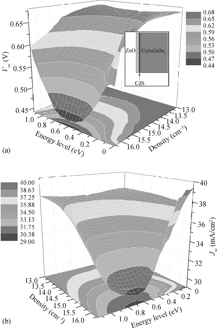
Fig. 1.
The variation of the (a) open-circuit voltage (Voc) and (b) shortcircuit current (Jsc) with defect state in CIGS. Inset of (a) is the structural model of a CIGS solar cell.
SEMICONDUCTOR DEVICES
Fucheng Wan1, Fuling Tang1, 2, , Hongtao Xue1, Wenjiang Lu1, 2, Yudong Feng2 and Zhiyuan Rui1
Corresponding author: Tang Fuling,tfl03@mails.tsinghua.edu.cn
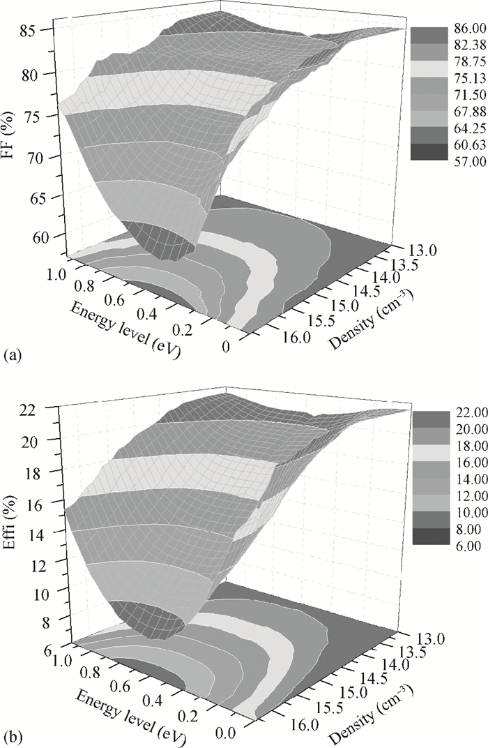
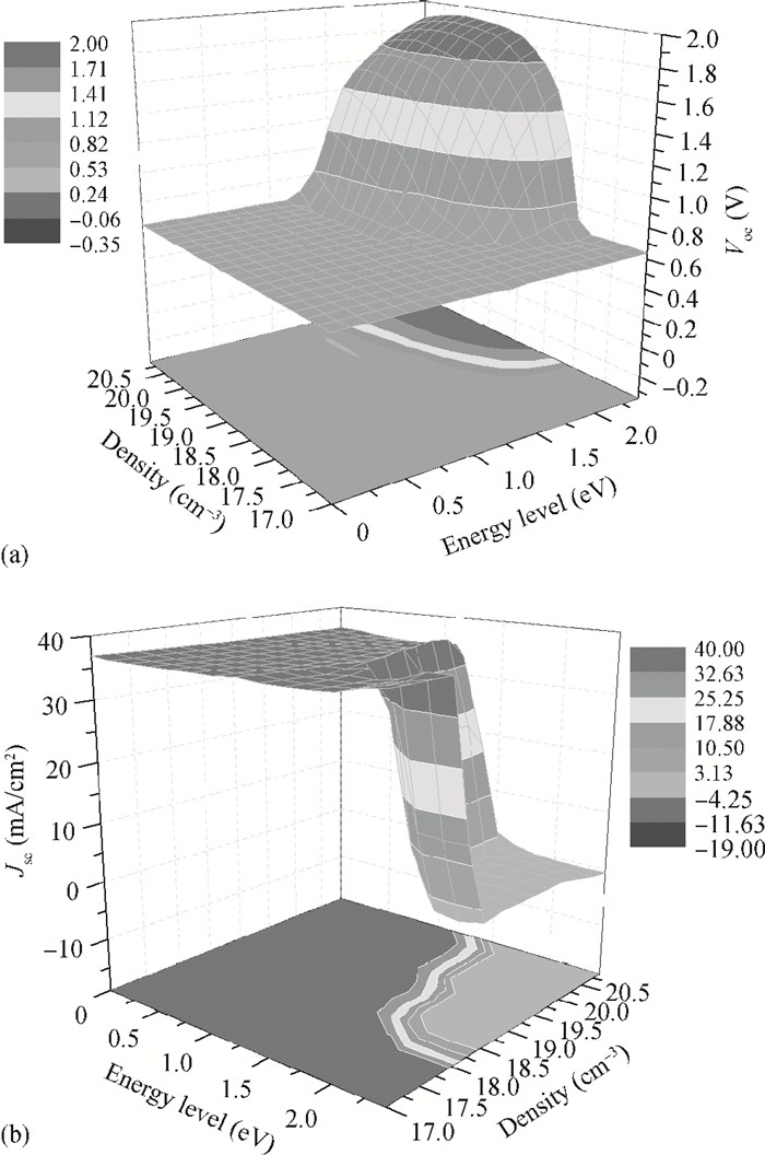
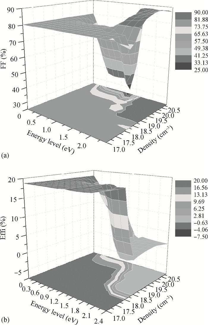
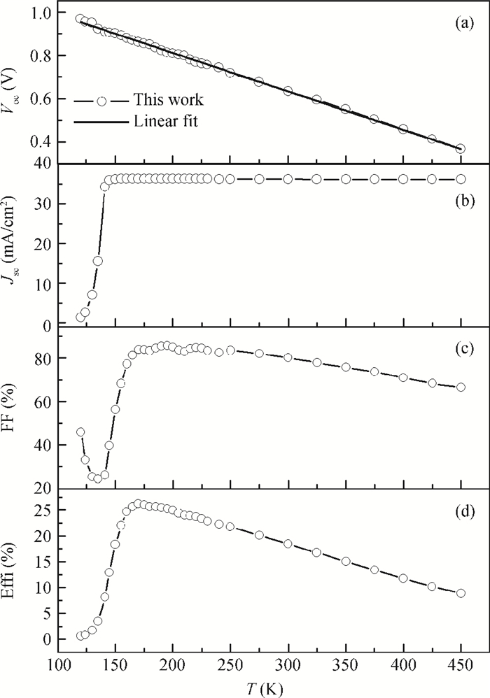
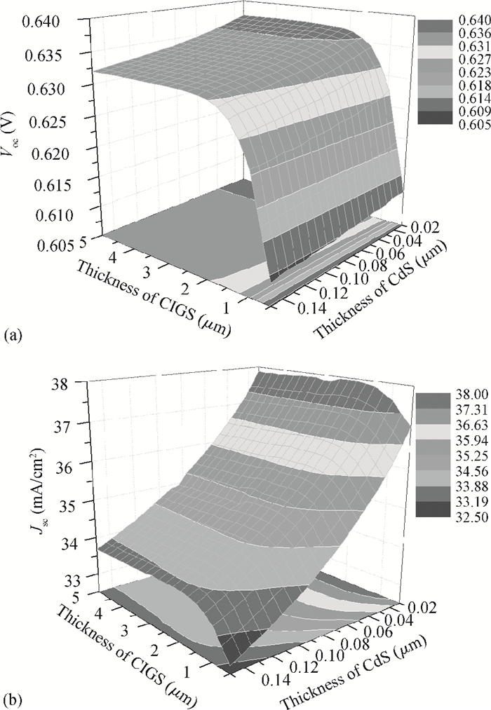
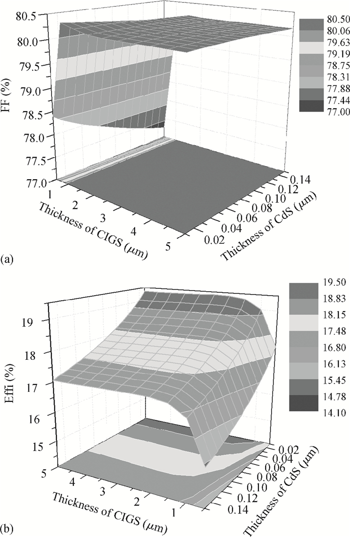
Abstract: Device modeling has been carried out to investigate the effects of defect states on the performance of ideal CuInGaSe2 (CIGS) thin film solar cells theoretically. The varieties of defect states (location in the band gap and densities) in absorption layer CIGS and in buffer layer CdS were examined. The performance parameters:open-circuit voltage, short-circuit current, fill factor, and photoelectric conversion efficiency for different defect states were quantitatively analyzed. We found that defect states always harm the performance of CIGS solar cells, but when defect state density is less than 1014 cm-3 in CIGS or less than 1018 cm-3 in CdS, defect states have little effect on the performances. When defect states are located in the middle of the band gap, they are more harmful. The effects of temperature and thickness are also considered. We found that CIGS solar cells have optimal performance at about 170 K and 2 μm of CIGS is enough for solar light absorption.
Keywords: device modeling, defect states, solar cell, conversion efficiency
| [1] |
Chen X, Zhao Y, Yao R, et al. Impact of lattice volume on the band gap broadening of isovalent S-doped CuInSe2. Journal of Semiconductors, 2008, 29:1883 doi: 10.1088/1674-4926/35/2/024011/pdf
|
| [2] |
Cao J, Qu S, Liu K, et al. Effect of bath temperature on the properties of CuInxGa1-xSe2 thin films grown by the electrodeposition technique. Journal of Semiconductors, 2010, 31:083003 doi: 10.1088/1674-4926/31/8/083003
|
| [3] |
Song J, Li S S, Huang C H, et al. Device modeling and simulation of the performance of Cu(In1-x, Gax)Se2 solar cells. Solid-State Electron, 2004, 48:73 doi: 10.1016/S0038-1101(03)00289-2
|
| [4] |
Bouloufa A, Djessas K, Zegadi A. Numerical simulation of CuInxGa1-xSe2 solar cells by AMPS-1D. Thin Solid Films, 2007, 515:6285 doi: 10.1016/j.tsf.2006.12.110
|
| [5] |
Novikov G F, Rabenok E V, Jeng M J, et al. The study of loss kinetics of current carriers in copper-indium-gallium selenide by microwave photoconductivity method. Journal of Renewable Sustainable Energy, 2012, 4:011604 doi: 10.1063/1.3670408
|
| [6] |
Ishizuka S, Yamada A, Fons P, et al. Flexible Cu(In,Ga)Se2 solar cells fabricated using alkali-silicate glass thin layers as an alkali source material. Journal Renewable Sustainable Energy, 2009, 1:013102 doi: 10.1063/1.3005376
|
| [7] |
Chu S, Majumdar A. Opportunities and challenges for a sustainable energy future. Nature, 2012, 488:294 doi: 10.1038/nature11475
|
| [8] |
Ramanathan K, Contreras M A, Perkins C L, et al. Properties of 19.2% efficiency ZnO/CdS/CuInGaSe2 thin-film solar cells. Progress in Photovoltaics:Research and Applications, 2003, 11:225 doi: 10.1002/(ISSN)1099-159X
|
| [9] |
Lin A G, Ding J N, Yuan N Y, et al. Analysis of the p+/p window layer of thin film solar cells by simulation. Journal of Semiconductors, 2012, 33:023002 doi: 10.1088/1674-4926/33/2/023002
|
| [10] |
Datta A, Damon-Lacoste J, Cabarrocas P R, et al. Defect states on the surfaces of a P-type c-Si wafer and how they control the performance of a double heterojunction solar cell. Solar Energy Materials and Solar Cells, 2008, 92:1500 doi: 10.1016/j.solmat.2008.06.015
|
| [11] |
Datta A, Damon-Lacoste J, Nath M, et al. Dominant role of interfaces in solar cells with N-a-Si:H/P-c-Si heterojunction with intrinsic thin layer. Mater Sci Eng B, 2009, 159:10 http://linkinghub.elsevier.com/retrieve/pii/S136403211200384X
|
| [12] |
Wei S H, Zunger A. Band offsets and optical bowings of chalcopyrites and Zn-based Ⅱ-Ⅵ alloys. J Appl Phys, 1995, 78:3846 doi: 10.1063/1.359901
|
| [13] |
Schroeder D J, Hernandez J L, Rockett A A. Point defects and hole transport in epitaxial CuIn1-xGaxSe2. Ternary and Multinary Compounds:Proceedings of the 11th International Conference on Ternary and Multinary Compounds, 1999:749
|
| [14] |
Hanna G, Jasenek A, Rau U, et al. Influence of the Ga-content on the bulk defect densities of Cu(In,Ga)Se2. Thin Solid Films, 2001, 387:71 doi: 10.1016/S0040-6090(00)01710-7
|
| [15] |
Tang F L, Zhu Z X, Xue H T, et al. Optical properties of Al-doped CuInSe2 from the first principle calculation. Physica B, 2012, 407:4814 doi: 10.1016/j.physb.2012.09.015
|
| [16] |
Xue H T, Lu W J, Zhu Z X, et al. Al-doped CuInSe2:an ab initio study of structural and electronic properties of a photovoltaic material. Advanced Materials Research, 2012, 512-515:1543 doi: 10.4028/www.scientific.net/AMR.512-515
|
| [17] |
Xue H T, Tang F L, Lu W J, et al. First-principles investigation of structural phase transitions and electronic properties of CuGaSe2 up to 100 GPa. Computational Materials Science, 2013, 67:21 doi: 10.1016/j.commatsci.2012.08.031
|
| [18] |
Wan F C, Tang F L, Zhu Z X, et al. First-princip les investig ation of the optical properties of CuIn(SxSe1-x)2. Materials Science in Semiconductor Processing, 2013, 16:1422 doi: 10.1016/j.mssp.2013.05.009
|
| [19] |
Hinuma Y, Oba F, Kumagai Y, et al. Band offsets of CuInSe2/CdS and CuInSe2/ZnS (110) interfaces:a hybrid density functional theory study. Phys Rev B, 2013, 88:035305 doi: 10.1103/PhysRevB.88.035305
|
| [20] |
Dharmadasa I M. Fermi level pinning and effects on CuInGaSe2-based thin-film solar cells. Semicond Sci Technol, 2009, 24:055016 doi: 10.1088/0268-1242/24/5/055016
|
| [21] |
Vaynzo Y, Bakulin A A, Gélinas S, et al. Direct observation of photoinduced bound charge-pair states at an organic-Inorganic semiconductor interface. Phys Rev Lett, 2012, 108:246605 doi: 10.1103/PhysRevLett.108.246605
|
| [22] |
Zhang S B, Wei S H, Zunger A. Stabilization of ternary compounds via ordered arrays of defect pairs. Phys Rev Lett, 1997, 78:4059 doi: 10.1103/PhysRevLett.78.4059
|
| [23] |
Zhang S B, Wei S H, Zunger A. Defect physics of the CuInSe2 chalcopyrite semiconductor. Phys Rev B, 1998, 57:9642 doi: 10.1103/PhysRevB.57.9642
|
| [24] |
Sugiyama M, Nakai R, Nakanishi H, et al. Interface Fermi level pinning in a Cu/p-CuGaS2 Schottky diode. Journal of Physics and Chemistry of Solids, 2003, 64:1787 doi: 10.1016/S0022-3697(03)00144-6
|
| [25] |
Dharmadasa I M, Bunning J D, Samantilleke A P, et al. Effects of multi-defects at metal/semiconductor interfaces on electrical properties and their influence on stability and life time of thin film solar cells. Solar Energy Materials and Solar Cells, 2005, 86:373 doi: 10.1016/j.solmat.2004.08.009
|
| [26] |
Dullweber T, Hanna G, Shams-Kolahi W, et al. Study of the effect of gallium grading in Cu(In, Ga)Se2. Thin Solid Films, 2000, 361:478 http://cat.inist.fr/?aModele=afficheN&cpsidt=23729873
|
| [27] |
Dullweber T, Hanna G, Rau U, et al. A new approach to high-efficiency solar cells by band gap grading in Cu(In,Ga)Se2 chalcopyrite semiconductors. Solar Energy Materials and Solar Cells, 2001, 67:145 doi: 10.1016/S0927-0248(00)00274-9
|
| [28] |
Zhu H, Kalkan A K, Hou J, et al. Application of AMPS-1D for solar cell simulation. AIP Conference Proceedings, 1999, 462:309 https://iwe.pure.elsevier.com/en/publications/a-new-simulation-software-of-solar-cells-wxamps
|
| [29] |
NREL, solar Spectral Irradiance:Air Mass1.5, http://rredc.nrel.gov/solar/spectra/aml.5/
|


Article views: 3343 Times PDF downloads: 49 Times Cited by: 0 Times
Received: 13 July 2013 Revised: 14 August 2013 Online: Published: 01 February 2014
| Citation: |
Fucheng Wan, Fuling Tang, Hongtao Xue, Wenjiang Lu, Yudong Feng, Zhiyuan Rui. Effects of defect states on the performance of CuInGaSe2 solar cells[J]. Journal of Semiconductors, 2014, 35(2): 024011. doi: 10.1088/1674-4926/35/2/024011
****
F C Wan, F L Tang, H T Xue, W J Lu, Y D Feng, Z Y Rui. Effects of defect states on the performance of CuInGaSe2 solar cells[J]. J. Semicond., 2014, 35(2): 024011. doi: 10.1088/1674-4926/35/2/024011.

|
| [1] |
Chen X, Zhao Y, Yao R, et al. Impact of lattice volume on the band gap broadening of isovalent S-doped CuInSe2. Journal of Semiconductors, 2008, 29:1883 doi: 10.1088/1674-4926/35/2/024011/pdf
|
| [2] |
Cao J, Qu S, Liu K, et al. Effect of bath temperature on the properties of CuInxGa1-xSe2 thin films grown by the electrodeposition technique. Journal of Semiconductors, 2010, 31:083003 doi: 10.1088/1674-4926/31/8/083003
|
| [3] |
Song J, Li S S, Huang C H, et al. Device modeling and simulation of the performance of Cu(In1-x, Gax)Se2 solar cells. Solid-State Electron, 2004, 48:73 doi: 10.1016/S0038-1101(03)00289-2
|
| [4] |
Bouloufa A, Djessas K, Zegadi A. Numerical simulation of CuInxGa1-xSe2 solar cells by AMPS-1D. Thin Solid Films, 2007, 515:6285 doi: 10.1016/j.tsf.2006.12.110
|
| [5] |
Novikov G F, Rabenok E V, Jeng M J, et al. The study of loss kinetics of current carriers in copper-indium-gallium selenide by microwave photoconductivity method. Journal of Renewable Sustainable Energy, 2012, 4:011604 doi: 10.1063/1.3670408
|
| [6] |
Ishizuka S, Yamada A, Fons P, et al. Flexible Cu(In,Ga)Se2 solar cells fabricated using alkali-silicate glass thin layers as an alkali source material. Journal Renewable Sustainable Energy, 2009, 1:013102 doi: 10.1063/1.3005376
|
| [7] |
Chu S, Majumdar A. Opportunities and challenges for a sustainable energy future. Nature, 2012, 488:294 doi: 10.1038/nature11475
|
| [8] |
Ramanathan K, Contreras M A, Perkins C L, et al. Properties of 19.2% efficiency ZnO/CdS/CuInGaSe2 thin-film solar cells. Progress in Photovoltaics:Research and Applications, 2003, 11:225 doi: 10.1002/(ISSN)1099-159X
|
| [9] |
Lin A G, Ding J N, Yuan N Y, et al. Analysis of the p+/p window layer of thin film solar cells by simulation. Journal of Semiconductors, 2012, 33:023002 doi: 10.1088/1674-4926/33/2/023002
|
| [10] |
Datta A, Damon-Lacoste J, Cabarrocas P R, et al. Defect states on the surfaces of a P-type c-Si wafer and how they control the performance of a double heterojunction solar cell. Solar Energy Materials and Solar Cells, 2008, 92:1500 doi: 10.1016/j.solmat.2008.06.015
|
| [11] |
Datta A, Damon-Lacoste J, Nath M, et al. Dominant role of interfaces in solar cells with N-a-Si:H/P-c-Si heterojunction with intrinsic thin layer. Mater Sci Eng B, 2009, 159:10 http://linkinghub.elsevier.com/retrieve/pii/S136403211200384X
|
| [12] |
Wei S H, Zunger A. Band offsets and optical bowings of chalcopyrites and Zn-based Ⅱ-Ⅵ alloys. J Appl Phys, 1995, 78:3846 doi: 10.1063/1.359901
|
| [13] |
Schroeder D J, Hernandez J L, Rockett A A. Point defects and hole transport in epitaxial CuIn1-xGaxSe2. Ternary and Multinary Compounds:Proceedings of the 11th International Conference on Ternary and Multinary Compounds, 1999:749
|
| [14] |
Hanna G, Jasenek A, Rau U, et al. Influence of the Ga-content on the bulk defect densities of Cu(In,Ga)Se2. Thin Solid Films, 2001, 387:71 doi: 10.1016/S0040-6090(00)01710-7
|
| [15] |
Tang F L, Zhu Z X, Xue H T, et al. Optical properties of Al-doped CuInSe2 from the first principle calculation. Physica B, 2012, 407:4814 doi: 10.1016/j.physb.2012.09.015
|
| [16] |
Xue H T, Lu W J, Zhu Z X, et al. Al-doped CuInSe2:an ab initio study of structural and electronic properties of a photovoltaic material. Advanced Materials Research, 2012, 512-515:1543 doi: 10.4028/www.scientific.net/AMR.512-515
|
| [17] |
Xue H T, Tang F L, Lu W J, et al. First-principles investigation of structural phase transitions and electronic properties of CuGaSe2 up to 100 GPa. Computational Materials Science, 2013, 67:21 doi: 10.1016/j.commatsci.2012.08.031
|
| [18] |
Wan F C, Tang F L, Zhu Z X, et al. First-princip les investig ation of the optical properties of CuIn(SxSe1-x)2. Materials Science in Semiconductor Processing, 2013, 16:1422 doi: 10.1016/j.mssp.2013.05.009
|
| [19] |
Hinuma Y, Oba F, Kumagai Y, et al. Band offsets of CuInSe2/CdS and CuInSe2/ZnS (110) interfaces:a hybrid density functional theory study. Phys Rev B, 2013, 88:035305 doi: 10.1103/PhysRevB.88.035305
|
| [20] |
Dharmadasa I M. Fermi level pinning and effects on CuInGaSe2-based thin-film solar cells. Semicond Sci Technol, 2009, 24:055016 doi: 10.1088/0268-1242/24/5/055016
|
| [21] |
Vaynzo Y, Bakulin A A, Gélinas S, et al. Direct observation of photoinduced bound charge-pair states at an organic-Inorganic semiconductor interface. Phys Rev Lett, 2012, 108:246605 doi: 10.1103/PhysRevLett.108.246605
|
| [22] |
Zhang S B, Wei S H, Zunger A. Stabilization of ternary compounds via ordered arrays of defect pairs. Phys Rev Lett, 1997, 78:4059 doi: 10.1103/PhysRevLett.78.4059
|
| [23] |
Zhang S B, Wei S H, Zunger A. Defect physics of the CuInSe2 chalcopyrite semiconductor. Phys Rev B, 1998, 57:9642 doi: 10.1103/PhysRevB.57.9642
|
| [24] |
Sugiyama M, Nakai R, Nakanishi H, et al. Interface Fermi level pinning in a Cu/p-CuGaS2 Schottky diode. Journal of Physics and Chemistry of Solids, 2003, 64:1787 doi: 10.1016/S0022-3697(03)00144-6
|
| [25] |
Dharmadasa I M, Bunning J D, Samantilleke A P, et al. Effects of multi-defects at metal/semiconductor interfaces on electrical properties and their influence on stability and life time of thin film solar cells. Solar Energy Materials and Solar Cells, 2005, 86:373 doi: 10.1016/j.solmat.2004.08.009
|
| [26] |
Dullweber T, Hanna G, Shams-Kolahi W, et al. Study of the effect of gallium grading in Cu(In, Ga)Se2. Thin Solid Films, 2000, 361:478 http://cat.inist.fr/?aModele=afficheN&cpsidt=23729873
|
| [27] |
Dullweber T, Hanna G, Rau U, et al. A new approach to high-efficiency solar cells by band gap grading in Cu(In,Ga)Se2 chalcopyrite semiconductors. Solar Energy Materials and Solar Cells, 2001, 67:145 doi: 10.1016/S0927-0248(00)00274-9
|
| [28] |
Zhu H, Kalkan A K, Hou J, et al. Application of AMPS-1D for solar cell simulation. AIP Conference Proceedings, 1999, 462:309 https://iwe.pure.elsevier.com/en/publications/a-new-simulation-software-of-solar-cells-wxamps
|
| [29] |
NREL, solar Spectral Irradiance:Air Mass1.5, http://rredc.nrel.gov/solar/spectra/aml.5/
|

 WeChat ID
Journal of Semiconductors © 2017 All Rights Reserved 京ICP备05085259号-2

 DownLoad:

