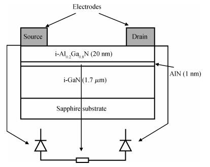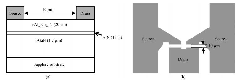
Fig. 1.
(a) Cross sectional and (b) top view of the fabricated sample. The grey regions show ohmic contact electrodes
SEMICONDUCTOR TECHNOLOGY
Yanxu Zhu1, , Weiwei Cao1, Yuyu Fan2, Ye Deng1 and Chen Xu1
Corresponding author: Zhu Yanxu, Email:zhuyx@bjut.edu.cn
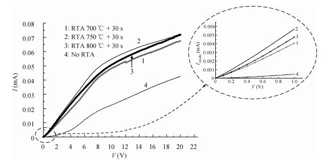
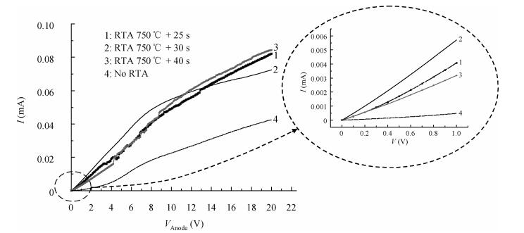
Abstract: Ohmic contacts with Ti/Al/Ti/Au source and drain electrodes on AlGaN/GaN high electron mobility transistors (HEMTs) were fabricated and subjected to rapid thermal annealing (RTA) in flowing N2. The wafer was divided into 5 parts and three of them were annealed for 30 s at 700, 750, and 800℃, respectively, the others were annealed at 750℃ for 25 and 40 s. Due to the RTA, a change from Schottky contact to Ohmic contact has been obtained between the electrode layer and the AlGaN/GaN heterojunction layer. We have achieved a low specific contact resistance of 7.41×10⁻⁶ Ω·cm2 and contact resistance of 0.54 Ω·mm measured by transmission line mode (TLM), and good surface morphology and edge acuity are also desirable by annealing at 750℃ for 30 s. The experiments also indicate that the performance of ohmic contact is first improved, then it reaches a peak, finally degrading with annealing temperature or annealing time rising.
Keywords: AlGaN/GaN HEMT, RTA, ohmic contact
| [1] |
Wang Jianhui, Wang Xinhua, Pang Lei, et al. Effect of varying layouts on the gate temperature for multi-finger AlGaN/GaN HEMTs. Journal of Semiconductors, 2012, 33(9):094004 doi: 10.1088/1674-4926/33/9/094004
|
| [2] |
Shen L, Heikman S, Moran B, et al. AlGaN/AlN/GaN high-power microwave HEMT. IEEE Electron Device Lett, 2001, 22(10):457 doi: 10.1109/55.954910
|
| [3] |
Long Fei, Du Jiangfeng, Luo Qian, et al. A research on current collapse of GaN HEMTs under DC high voltage. Chinese Journal of Semiconductors, 2006, 27(z1):227
|
| [4] |
Liu Guoguo, Zheng Yingkui, Wei Ke, et al. An 8W X band AlGaN/GaN power HEMT. Journal of Semiconductors, 2008, 29(7):1354 http://www.jos.ac.cn/bdtxben/ch/reader/view_abstract.aspx?file_no=07103001&flag=1
|
| [5] |
Shen L, Coffie R, Buttari D, et al. High-power polarization-engineered GaN/AlGaN/GaN HEMTs without surface passivation. IEEE Electron Device Lett, 2004, 25(1):7 doi: 10.1109/LED.2003.821673
|
| [6] |
Suita M, Nanjo T, Oishi T, et al. Ion implantation doping for AlGaN/GaN HEMTs. Bremen, Germany:Wiley-VCH Verlag, 2006 doi: 10.1002/pssc.200565135/references
|
| [7] |
Wang L, Kim D, Adesida I. Direct contact mechanism of ohmic metallization to AlGaN/GaN heterostructures via ohmic area recess etching. Appl Phys Lett, 2009, 95(17):172107 doi: 10.1063/1.3255014
|
| [8] |
Van Daele B, Van Tendeloo G, Derluyn J, et al. Mechanism for ohmic contact formation on Si3N4 passivated AlGaN/GaN high-electron-mobility transistors. Appl Phys Lett, 2006, 89(20):190820 http://cat.inist.fr/?aModele=afficheN&cpsidt=18361176
|
| [9] |
Bardwell J A, Haffouz S, Tang H, et al. Electrical characterization and surface morphology of optimized Ti/Al/Ti/Au ohmic contacts for AlGaN/GaN HEMTs. J Electrochem Soc, 2006, 153(8):G746 doi: 10.1149/1.2206998
|
| [10] |
Miller M A, Mohney S E. V/Al/V/Ag ohmic contacts to n-AlGaN/GaN heterostructures with a thin GaN cap. Appl Phys Lett, 2007, 91:121031 http://cat.inist.fr/?aModele=afficheN&cpsidt=18970790
|
| [11] |
Gong R, Wang J, Dong Z, et al. Analysis on the new mechanisms of low resistance stacked Ti/Al ohmic contact structure on AlGaN/GaN HEMTs. J Phys D:Appl Phys, 2010, 43(39):395102 doi: 10.1088/0022-3727/43/39/395102
|
| [12] |
Smorchkova I P, Chen L, Mates T, et al. AlN/GaN and (Al, Ga)N/AlN/GaN two-dimensional electron gas structures grown by plasma-assisted molecular-beam epitaxy. J Appl Phys, 2001, 90(10):5196 doi: 10.1063/1.1412273
|
| [13] |
Kaun S W, Wong M H, Mishra U K, et al. Correlation between threading dislocation density and sheet resistance of AlGaN/AlN/GaN heterostructures grown by plasma-assisted molecular beam epitaxy. Appl Phys Lett, 2012, 100(26):210226 doi: 10.1063/1.4730951?journalCode=apl
|


Article views: 4937 Times PDF downloads: 152 Times Cited by: 0 Times
Received: 04 July 2013 Revised: 11 September 2013 Online: Published: 01 February 2014
| Citation: |
Yanxu Zhu, Weiwei Cao, Yuyu Fan, Ye Deng, Chen Xu. Effects of rapid thermal annealing on ohmic contact of AlGaN/GaN HEMTs[J]. Journal of Semiconductors, 2014, 35(2): 026004. doi: 10.1088/1674-4926/35/2/026004
****
Y X Zhu, W W Cao, Y Y Fan, Y Deng, C Xu. Effects of rapid thermal annealing on ohmic contact of AlGaN/GaN HEMTs[J]. J. Semicond., 2014, 35(2): 026004. doi: 10.1088/1674-4926/35/2/026004.

|
| [1] |
Wang Jianhui, Wang Xinhua, Pang Lei, et al. Effect of varying layouts on the gate temperature for multi-finger AlGaN/GaN HEMTs. Journal of Semiconductors, 2012, 33(9):094004 doi: 10.1088/1674-4926/33/9/094004
|
| [2] |
Shen L, Heikman S, Moran B, et al. AlGaN/AlN/GaN high-power microwave HEMT. IEEE Electron Device Lett, 2001, 22(10):457 doi: 10.1109/55.954910
|
| [3] |
Long Fei, Du Jiangfeng, Luo Qian, et al. A research on current collapse of GaN HEMTs under DC high voltage. Chinese Journal of Semiconductors, 2006, 27(z1):227
|
| [4] |
Liu Guoguo, Zheng Yingkui, Wei Ke, et al. An 8W X band AlGaN/GaN power HEMT. Journal of Semiconductors, 2008, 29(7):1354 http://www.jos.ac.cn/bdtxben/ch/reader/view_abstract.aspx?file_no=07103001&flag=1
|
| [5] |
Shen L, Coffie R, Buttari D, et al. High-power polarization-engineered GaN/AlGaN/GaN HEMTs without surface passivation. IEEE Electron Device Lett, 2004, 25(1):7 doi: 10.1109/LED.2003.821673
|
| [6] |
Suita M, Nanjo T, Oishi T, et al. Ion implantation doping for AlGaN/GaN HEMTs. Bremen, Germany:Wiley-VCH Verlag, 2006 doi: 10.1002/pssc.200565135/references
|
| [7] |
Wang L, Kim D, Adesida I. Direct contact mechanism of ohmic metallization to AlGaN/GaN heterostructures via ohmic area recess etching. Appl Phys Lett, 2009, 95(17):172107 doi: 10.1063/1.3255014
|
| [8] |
Van Daele B, Van Tendeloo G, Derluyn J, et al. Mechanism for ohmic contact formation on Si3N4 passivated AlGaN/GaN high-electron-mobility transistors. Appl Phys Lett, 2006, 89(20):190820 http://cat.inist.fr/?aModele=afficheN&cpsidt=18361176
|
| [9] |
Bardwell J A, Haffouz S, Tang H, et al. Electrical characterization and surface morphology of optimized Ti/Al/Ti/Au ohmic contacts for AlGaN/GaN HEMTs. J Electrochem Soc, 2006, 153(8):G746 doi: 10.1149/1.2206998
|
| [10] |
Miller M A, Mohney S E. V/Al/V/Ag ohmic contacts to n-AlGaN/GaN heterostructures with a thin GaN cap. Appl Phys Lett, 2007, 91:121031 http://cat.inist.fr/?aModele=afficheN&cpsidt=18970790
|
| [11] |
Gong R, Wang J, Dong Z, et al. Analysis on the new mechanisms of low resistance stacked Ti/Al ohmic contact structure on AlGaN/GaN HEMTs. J Phys D:Appl Phys, 2010, 43(39):395102 doi: 10.1088/0022-3727/43/39/395102
|
| [12] |
Smorchkova I P, Chen L, Mates T, et al. AlN/GaN and (Al, Ga)N/AlN/GaN two-dimensional electron gas structures grown by plasma-assisted molecular-beam epitaxy. J Appl Phys, 2001, 90(10):5196 doi: 10.1063/1.1412273
|
| [13] |
Kaun S W, Wong M H, Mishra U K, et al. Correlation between threading dislocation density and sheet resistance of AlGaN/AlN/GaN heterostructures grown by plasma-assisted molecular beam epitaxy. Appl Phys Lett, 2012, 100(26):210226 doi: 10.1063/1.4730951?journalCode=apl
|

 WeChat ID
Journal of Semiconductors © 2017 All Rights Reserved 京ICP备05085259号-2

 DownLoad: