


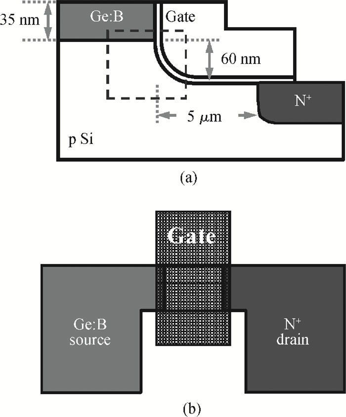
Fig. 1.
(a) Schematic of a TFET with a Ge:B source and an L-shaped channel formed on Si substrate. (b) Schematic top view of the TFET.
SEMICONDUCTOR DEVICES
Yan Liu, Jing Yan, Hongjuan Wang and Genquan Han
Corresponding author: Han Genquan, hangenquan@ieee.org, hangenquan@cqu.edu.cn
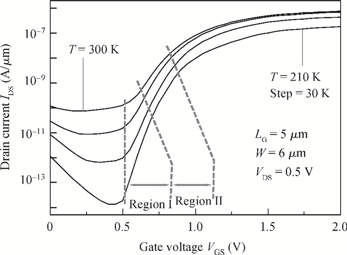
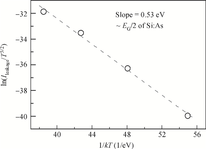
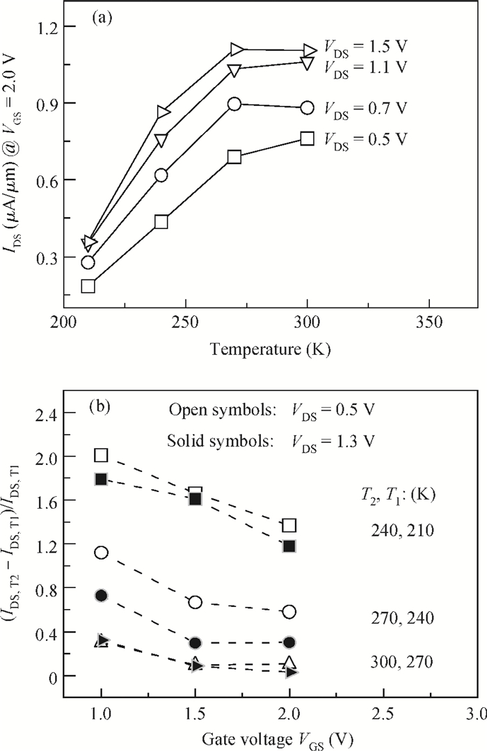
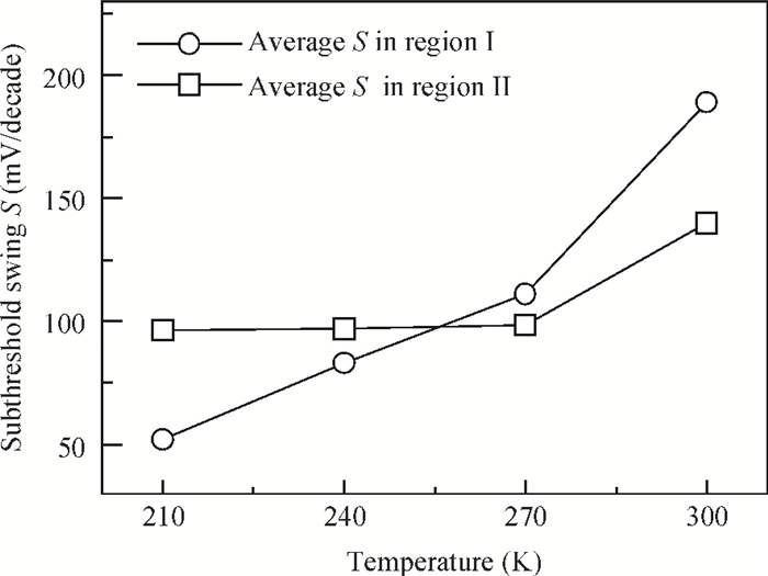
Abstract: We fabricated n-type Si-based TFETs with a Ge source on Si(110) substrate. The temperature dependent IDS-VGS characteristics of a TFET formed on Si(110) are investigated in the temperature range of 210 to 300 K. A study of the temperature dependence of $I_{\rm Leakage}$ indicates that $I_{\rm Leakage}$ is mainly dominated by the Shockley-Read-Hall (SRH) generation-recombination current of the n+ drain-Si substrate junction. $I_{\rm ON}$ increases monotonically with temperature, which is attributed to a reduction of the bandgap at the tunneling junction and an enhancement of band-to-band tunneling rate. The subthreshold swing S for trap assisted tunneling (TAT) current and band-to-band tunneling (BTBT) current shows the different temperature dependence. The subthreshold swing S for the TAT current degrades with temperature, while the S for BTBT current is temperature independent.
Keywords: tunneling field-effect-transistor, band-to-band tunneling, germanium, tunneling, temperature
| [1] |
Hu C, Patel P, Bowonder A, et al. Prospect of tunneling green transistor for 0. 1 V CMOS. IEEE International Electron Devices Meeting (IEDM), 2010: 387 http://nano.eecs.berkeley.edu/publications/IEDM_2010_TFET.pdf
|
| [2] |
Ionescu A M, Riel H. Tunnel field-effect transistors as energy-efficient electronic switches. Nature, 2011, 479:329 doi: 10.1038/nature10679
|
| [3] |
Han G, Guo P, Yang Y, et al. Silicon-based tunneling field-effect transistor with elevated germanium source formed on (110) silicon substrate. Appl Phys Lett, 2011, 98:153502 doi: 10.1063/1.3579242
|
| [4] |
Yang Y, Su S, Guo P, et al. Towards direct band-to-band tunneling in p-channel tunneling field effect transistor (TFET): technology enablement by germanium-tin (GeSn). IEEE International Electron Devices Meeting (IEDM), 2012: 379 http://ieeexplore.ieee.org/document/6479053/l
|
| [5] |
Han G, Guo P, Yang Y, et al. Source engineering for tunnel field-effect transistor:elevated source with vertical silicon-germanium/germanium heterostructure. Jpn J Appl Phys, 2011, 50:04DJ07 doi: 10.1143/JJAP.50.04DJ07/pdf
|
| [6] |
Guo P F, Yang L T, Yang Y, et al. Tunneling field effect transistor:effect of strain and temperature on tunneling current. IEEE Electron Device Lett, 2009, 30:981 doi: 10.1109/LED.2009.2026296
|
| [7] |
Liu Y, Wang H, Yan J, et al. Silicon tunnel field-effect transistor with in situ doped single crystalline Ge source for achieving sub-60 mV/decade subthreshold swing. Chin Phys Lett, 2013, 30:088502 doi: 10.1088/0256-307X/30/8/088502
|
| [8] |
Jeon K, Loh W Y, Patel P, et al. Si tunnel transistors with a novel silicided source and 46 mV/dec swing. Symposium on VLSI Technology, 2010: 121 http://ieeexplore.ieee.org/document/5556195/
|
| [9] |
Han G, Yee Y S, Guo P, et al. Enhancement of TFET performance using dopant profile steepening implant and source dopant concentration engineering at tunneling junction. Silicon Nanoelectronics Workshop, 2010 http://ieeexplore.ieee.org/document/5562594/
|
| [10] |
Toh E H, Wang G H, Chan L, et al. Device design and scalability of a double-gate tunneling field-effect transistor with silicon-germanium source. Jpn J Appl Phys, 2007, 46:2593 doi: 10.1143/JJAP.47.2593/meta
|
| [11] |
Knoch J, Appenzeller J. Modeling of high-performance p-type Ⅲ-Ⅴ heterojunction tunnel FETs. IEEE Electron Device Lett, 2010, 31:305 doi: 10.1109/LED.2010.2041180
|
| [12] |
Mookerjea S, Mohata D, Mayer T, et al. Temperature-dependent Ⅳ characteristics of a vertical In0. 53Ga0. 47As tunnel FET. IEEE Electron Device Lett, 2010, 31: 564 http://www.ndcl.ee.psu.edu/papers/75_Mookerjea_EDL_2010.pdf
|
| [13] |
Kane E O. Zener tunneling in semiconductors. J Phys Chem Solids, 1960, 12:181 doi: 10.1016/0022-3697(60)90035-4
|
| [14] |
Zhang Q, Zhao W, Seabaugh A. Analytic expression and approach for low-subthreshold-swing tunnel transistors. Device Research Conference Digest, 2005: 161 http://ieeexplore.ieee.org/document/1553102/
|


Article views: 3877 Times PDF downloads: 18 Times Cited by: 0 Times
Received: 21 July 2013 Revised: 30 August 2013 Online: Published: 01 February 2014
| Citation: |
Yan Liu, Jing Yan, Hongjuan Wang, Genquan Han. Temperature dependent IDS-VGS characteristics of an N-channel Si tunneling field-effect transistor with a germanium source on Si(110) substrate[J]. Journal of Semiconductors, 2014, 35(2): 024001. doi: 10.1088/1674-4926/35/2/024001
****
Y Liu, J Yan, H J Wang, G Q Han. Temperature dependent IDS-VGS characteristics of an N-channel Si tunneling field-effect transistor with a germanium source on Si(110) substrate[J]. J. Semicond., 2014, 35(2): 024001. doi: 10.1088/1674-4926/35/2/024001.

|
| [1] |
Hu C, Patel P, Bowonder A, et al. Prospect of tunneling green transistor for 0. 1 V CMOS. IEEE International Electron Devices Meeting (IEDM), 2010: 387 http://nano.eecs.berkeley.edu/publications/IEDM_2010_TFET.pdf
|
| [2] |
Ionescu A M, Riel H. Tunnel field-effect transistors as energy-efficient electronic switches. Nature, 2011, 479:329 doi: 10.1038/nature10679
|
| [3] |
Han G, Guo P, Yang Y, et al. Silicon-based tunneling field-effect transistor with elevated germanium source formed on (110) silicon substrate. Appl Phys Lett, 2011, 98:153502 doi: 10.1063/1.3579242
|
| [4] |
Yang Y, Su S, Guo P, et al. Towards direct band-to-band tunneling in p-channel tunneling field effect transistor (TFET): technology enablement by germanium-tin (GeSn). IEEE International Electron Devices Meeting (IEDM), 2012: 379 http://ieeexplore.ieee.org/document/6479053/l
|
| [5] |
Han G, Guo P, Yang Y, et al. Source engineering for tunnel field-effect transistor:elevated source with vertical silicon-germanium/germanium heterostructure. Jpn J Appl Phys, 2011, 50:04DJ07 doi: 10.1143/JJAP.50.04DJ07/pdf
|
| [6] |
Guo P F, Yang L T, Yang Y, et al. Tunneling field effect transistor:effect of strain and temperature on tunneling current. IEEE Electron Device Lett, 2009, 30:981 doi: 10.1109/LED.2009.2026296
|
| [7] |
Liu Y, Wang H, Yan J, et al. Silicon tunnel field-effect transistor with in situ doped single crystalline Ge source for achieving sub-60 mV/decade subthreshold swing. Chin Phys Lett, 2013, 30:088502 doi: 10.1088/0256-307X/30/8/088502
|
| [8] |
Jeon K, Loh W Y, Patel P, et al. Si tunnel transistors with a novel silicided source and 46 mV/dec swing. Symposium on VLSI Technology, 2010: 121 http://ieeexplore.ieee.org/document/5556195/
|
| [9] |
Han G, Yee Y S, Guo P, et al. Enhancement of TFET performance using dopant profile steepening implant and source dopant concentration engineering at tunneling junction. Silicon Nanoelectronics Workshop, 2010 http://ieeexplore.ieee.org/document/5562594/
|
| [10] |
Toh E H, Wang G H, Chan L, et al. Device design and scalability of a double-gate tunneling field-effect transistor with silicon-germanium source. Jpn J Appl Phys, 2007, 46:2593 doi: 10.1143/JJAP.47.2593/meta
|
| [11] |
Knoch J, Appenzeller J. Modeling of high-performance p-type Ⅲ-Ⅴ heterojunction tunnel FETs. IEEE Electron Device Lett, 2010, 31:305 doi: 10.1109/LED.2010.2041180
|
| [12] |
Mookerjea S, Mohata D, Mayer T, et al. Temperature-dependent Ⅳ characteristics of a vertical In0. 53Ga0. 47As tunnel FET. IEEE Electron Device Lett, 2010, 31: 564 http://www.ndcl.ee.psu.edu/papers/75_Mookerjea_EDL_2010.pdf
|
| [13] |
Kane E O. Zener tunneling in semiconductors. J Phys Chem Solids, 1960, 12:181 doi: 10.1016/0022-3697(60)90035-4
|
| [14] |
Zhang Q, Zhao W, Seabaugh A. Analytic expression and approach for low-subthreshold-swing tunnel transistors. Device Research Conference Digest, 2005: 161 http://ieeexplore.ieee.org/document/1553102/
|

 WeChat ID
Journal of Semiconductors © 2017 All Rights Reserved 京ICP备05085259号-2

 DownLoad:

