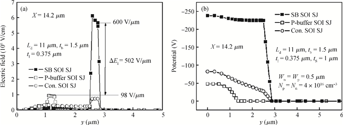
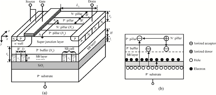
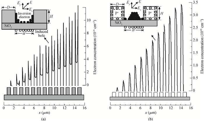
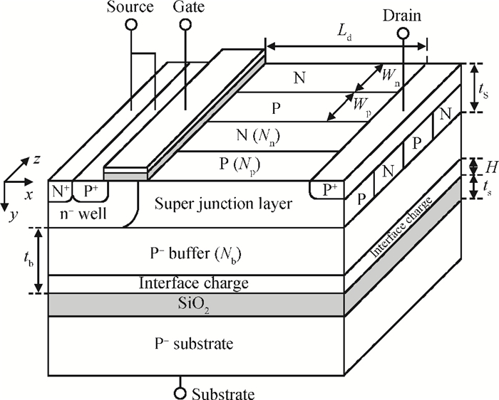
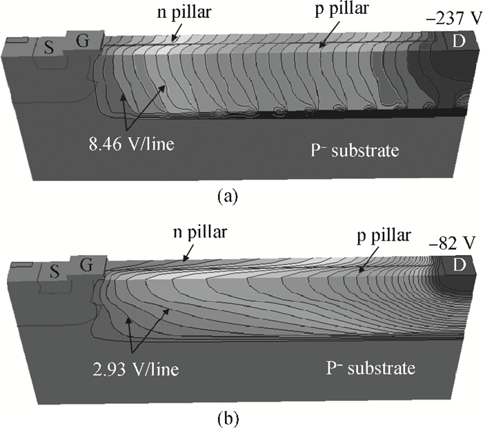
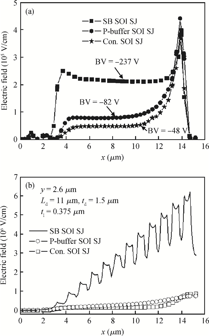
Citation: |
Lijuan Wu, Wentong Zhang, Bo Zhang, Zhaoji Li. A novel SOI high-voltage SJ-pLDMOS based on self-adaptive charge balance[J]. Journal of Semiconductors, 2014, 35(2): 024004. doi: 10.1088/1674-4926/35/2/024004
****
L J Wu, W T Zhang, B Zhang, Z J Li. A novel SOI high-voltage SJ-pLDMOS based on self-adaptive charge balance[J]. J. Semicond., 2014, 35(2): 024004. doi: 10.1088/1674-4926/35/2/024004.
|
A novel SOI high-voltage SJ-pLDMOS based on self-adaptive charge balance
DOI: 10.1088/1674-4926/35/2/024004
More Information
-
Abstract
A new SOI self-balance (SB) super-junction (SJ) pLDMOS with a self-adaptive charge (SAC) layer and its physical model are presented. The SB is an effective way to realize charges balance (CB). The substrate-assisted depletion (SAD) effect of the lateral SJ is eliminated by the self-adaptive inversion electrons provided by the SAC. At the same time, high concentration dynamic self-adaptive electrons effectively enhance the electric field (EI) of the dielectric buried layer and increase breakdown voltage (BV). EI=600 V/μm and BV=-237 V are obtained by 3D simulation on a 0.375-μm-thick dielectric layer and a 2.5-μm-thick top silicon layer. The optimized structure realizes the specific on resistance (Ron, sp) of 0.01319 Ω·cm2, FOM (FOM=BV2/Ron, sp) of 4.26 MW/cm2 under a 11 μm length (Ld) drift region. -
References
[1] Nassif-Khalil S G, Salama C A T. Super junction LDMOST in silicon-on-sapphire technology (SJ-LDMOST). Proc ISPSD, 2002:81 http://ieeexplore.ieee.org/abstract/document/1016176/[2] Ng R, Udrea F, Sheng K, et al. Lateral unbalanced super junction (USJ)/3D-RESURF for high breakdown voltage on SOI. Proc IEEE ISPSD, 2001:395 http://ieeexplore.ieee.org/document/934637/keywords[3] Chen Y, Buddharaju K D, Liang Y C, et al. Super junction power LDMOS on partial SOI platform. Proc ISPSD, California, USA, 2007:177 http://ieeexplore.ieee.org/document/5250425/[4] Chen W, Zhang B, Li Z. Optimization of super-junction SOI-LDMOS with a step doping surface-implanted layer. Semicond Sci Technol, 2007, 22(3):464 http://yadda.icm.edu.pl/yadda/element/bwmeta1.element.baztech-article-LOD6-0019-0001[5] Wang W, Zhang B, Li Z, et al. High-voltage SOI SJ-LDMOS with a nondepletion compensation layer. IEEE Electron Device Lett, 2009, 30(1):68 doi: 10.1109/LED.2008.2008208[6] Zhang B, Li Z, Hu S, et al. Field enhancement for dielectric layer of high-voltage devices on silicon on insulator. IEEE Trans Electron Devices, 2009, 56(10):2327 doi: 10.1109/TED.2009.2028405[7] Li Z, Luo X, Zhang B, et al. The enhancement of dielectric layer field of SOI high voltage devices. Fourth Joint Symposium on Opto-and Microelectronic Devices and Circuits, 2006:61 http://ieeexplore.ieee.org/abstract/document/4348285/[8] Luo Xiaorong, Zhang Bo, Li Zhaoji, et al. A novel SOI high voltage device structure with partial locating charge trench. Chinese Journal of Semiconductors, 2006, 27(1):115 http://en.cnki.com.cn/Article_en/CJFDTOTAL-BDTX200307015.htm[9] ISE TCAD Manuals. release 10. 0[10] Sze S M, Ng K K. Physics of semiconductor devices. 3rd ed. New York: A John Wiley and Sons, 2007 -
Proportional views