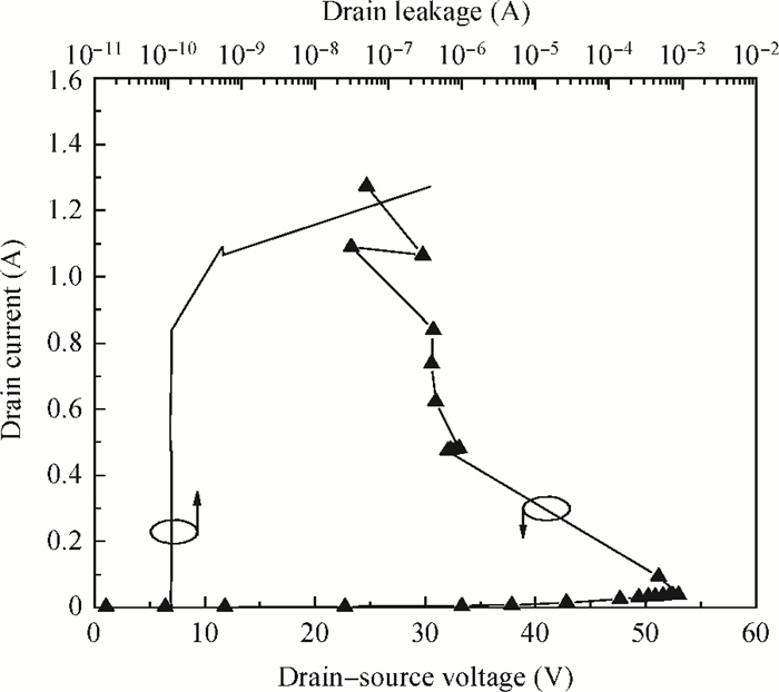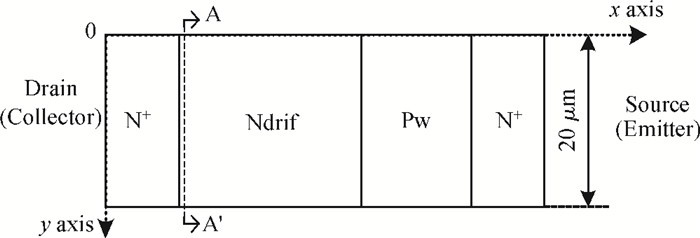
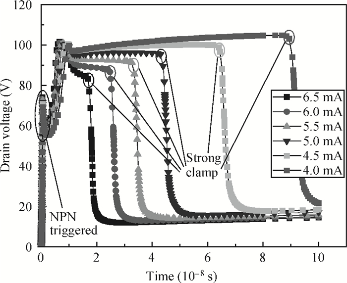
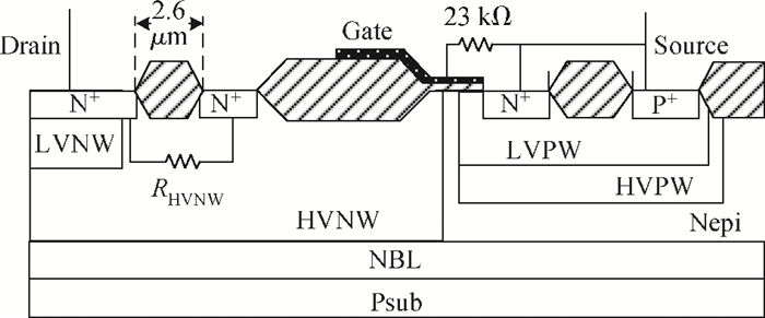
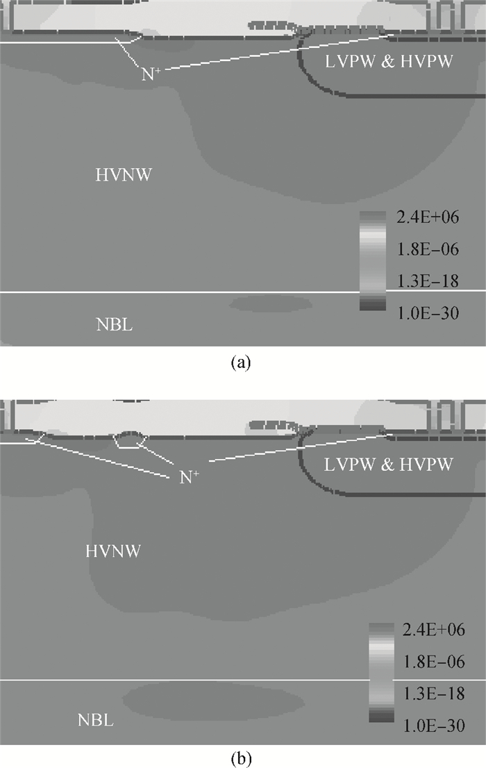
Fig. 1.
Cross sections of the conventional NLDMOS.
SEMICONDUCTOR DEVICES
Corresponding author: Fan Hang, fanmes@163.com
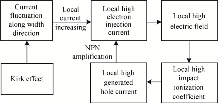
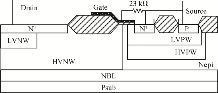
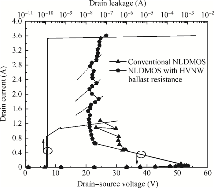
Abstract: To prevent the non-uniform conduction phenomenon caused by the Kirk effect in an NLDMOS under ESD stress, a novel NLDMOS structure is proposed. High electron injection current is the base of Kirk effect. Higher electron injection can makes the Kirk effect more serious and lead easily to the non-uniform conduction phenomenon. By splitting the drain N+ with the field oxide in the proposed structure, the crowded current can lead to a higher voltage drop on the ballast resistance. Therefore, the non-uniform conduction is suppressed, and its failure current is much improved.
Keywords: electro-static discharge, ballast resistance, LDMOS
| [1] |
Shrivastava M, Gossner H. A review on the ESD robustness of drain-extended MOS devices. J Device Mater Reliab, 2012, 12(4):615 doi: 10.1109/TDMR.2012.2220358
|
| [2] |
Voldman S H. ESD:physics and devices. John Wiley & Sons, Vermont, USA, 2004:105 doi: 10.1002/0470013508?systemMessage=Wiley+Online+Library+will+be+unavailable+on+Saturday+7th+Oct+from+03.00+EDT+%2F+08%3A00+BST+%2F+12%3A30+IST+%2F+15.00+SGT+to+08.00+EDT+%2F+13.00+BST+%2F+17%3A30+IST+%2F+20.00+SGT+and+Sunday+8th+Oct+from+03.00+EDT+%2F+08%3A00+BST+%2F+12%3A30+IST+%2F+15.00+SGT+to+06.00+EDT+%2F+11.00+BST+%2F+15%3A30+IST+%2F+18.00+SGT+for+essential+maintenance.+Apologies+for+the+inconvenience+caused+.
|
| [3] |
Wang C T, Ker M D, Tang T H, et al. ESD protection design with lateral DMOS transistor in 40-V BCD technology. Symp Int Physical and Failure Analysis of Integrated Circuits, 2010 http://ieeexplore.ieee.org/document/5604306/?isnumber=5621692&arnumber=5604306
|
| [4] |
Walker A J, Puchner H, Dhanraj S P. High-voltage CMOS ESD and the safe operating area. Electron Devices, 2009, 56(8):1753 doi: 10.1109/TED.2009.2022698
|
| [5] |
Ker M D, Lai T H. Investigation on robustness of CMOS devices against cable discharge event (CDE) under different layout parameters in a deep-submicrometer CMOS technology. IEEE Trans Electromag Compatibility, 2008, 50(4):810 doi: 10.1109/TEMC.2008.2004582
|
| [6] |
Lee J C, Hoque A, Croft G D, et al. An electrostatic discharge failure mechanism in semiconductor devices, with applications to electrostatic discharge measurements using transmission line pulsing technique. Solid-State Electron, 2000, 44(10):1771 doi: 10.1016/S0038-1101(00)00122-2
|
| [7] |
Chen W Y, Ker M D, Jou Y N, et al. Improvement on ESD robustness of lateral DMOS in high-voltage CMOS ICs by body current injection. Symp Int Circuits and Systems, 2009 http://ieeexplore.ieee.org/document/5117766/
|
| [8] |
Cao Y, Glaser U. Statically triggered active ESD clamps for high-voltage applications. Symp Electrical Overstress/Electrostatic Discharge (EOS/ESD), 2012 http://ieeexplore.ieee.org/document/6333329/
|
| [9] |
Ker M D, Ker M D, Shieh W T, et al. New ballasting layout schemes to improve ESD robustness of I/O buffers in fully silicided CMOS process. Electron Devices, 2009, 56(12):3149 doi: 10.1109/TED.2009.2031003
|


Article views: 3414 Times PDF downloads: 41 Times Cited by: 0 Times
Received: 03 July 2013 Revised: 22 August 2013 Online: Published: 01 February 2014
| Citation: |
Hang Fan, Bo Zhang. A novel NLDMOS with a high ballast resistance for ESD protection[J]. Journal of Semiconductors, 2014, 35(2): 024005. doi: 10.1088/1674-4926/35/2/024005
****
H Fan, B Zhang. A novel NLDMOS with a high ballast resistance for ESD protection[J]. J. Semicond., 2014, 35(2): 024005. doi: 10.1088/1674-4926/35/2/024005.

|
| [1] |
Shrivastava M, Gossner H. A review on the ESD robustness of drain-extended MOS devices. J Device Mater Reliab, 2012, 12(4):615 doi: 10.1109/TDMR.2012.2220358
|
| [2] |
Voldman S H. ESD:physics and devices. John Wiley & Sons, Vermont, USA, 2004:105 doi: 10.1002/0470013508?systemMessage=Wiley+Online+Library+will+be+unavailable+on+Saturday+7th+Oct+from+03.00+EDT+%2F+08%3A00+BST+%2F+12%3A30+IST+%2F+15.00+SGT+to+08.00+EDT+%2F+13.00+BST+%2F+17%3A30+IST+%2F+20.00+SGT+and+Sunday+8th+Oct+from+03.00+EDT+%2F+08%3A00+BST+%2F+12%3A30+IST+%2F+15.00+SGT+to+06.00+EDT+%2F+11.00+BST+%2F+15%3A30+IST+%2F+18.00+SGT+for+essential+maintenance.+Apologies+for+the+inconvenience+caused+.
|
| [3] |
Wang C T, Ker M D, Tang T H, et al. ESD protection design with lateral DMOS transistor in 40-V BCD technology. Symp Int Physical and Failure Analysis of Integrated Circuits, 2010 http://ieeexplore.ieee.org/document/5604306/?isnumber=5621692&arnumber=5604306
|
| [4] |
Walker A J, Puchner H, Dhanraj S P. High-voltage CMOS ESD and the safe operating area. Electron Devices, 2009, 56(8):1753 doi: 10.1109/TED.2009.2022698
|
| [5] |
Ker M D, Lai T H. Investigation on robustness of CMOS devices against cable discharge event (CDE) under different layout parameters in a deep-submicrometer CMOS technology. IEEE Trans Electromag Compatibility, 2008, 50(4):810 doi: 10.1109/TEMC.2008.2004582
|
| [6] |
Lee J C, Hoque A, Croft G D, et al. An electrostatic discharge failure mechanism in semiconductor devices, with applications to electrostatic discharge measurements using transmission line pulsing technique. Solid-State Electron, 2000, 44(10):1771 doi: 10.1016/S0038-1101(00)00122-2
|
| [7] |
Chen W Y, Ker M D, Jou Y N, et al. Improvement on ESD robustness of lateral DMOS in high-voltage CMOS ICs by body current injection. Symp Int Circuits and Systems, 2009 http://ieeexplore.ieee.org/document/5117766/
|
| [8] |
Cao Y, Glaser U. Statically triggered active ESD clamps for high-voltage applications. Symp Electrical Overstress/Electrostatic Discharge (EOS/ESD), 2012 http://ieeexplore.ieee.org/document/6333329/
|
| [9] |
Ker M D, Ker M D, Shieh W T, et al. New ballasting layout schemes to improve ESD robustness of I/O buffers in fully silicided CMOS process. Electron Devices, 2009, 56(12):3149 doi: 10.1109/TED.2009.2031003
|

 WeChat ID
Journal of Semiconductors © 2017 All Rights Reserved 京ICP备05085259号-2

 DownLoad: