Fig. 1.
(a) Schematic cross-section and (b) layout design of the SOI DTMOS.
SEMICONDUCTOR DEVICES
Xiaorong Luo1, 2, , Xiaowei Wang2, Gangyi Hu1, Yuanhang Fan2, Kun Zhou2, Yinchun Luo2, Ye Fan2, Zhengyuan Zhang1, Yong Mei1 and Bo Zhang2
Corresponding author: Luo Xiaorong, xrluo@uestc.edu.cn
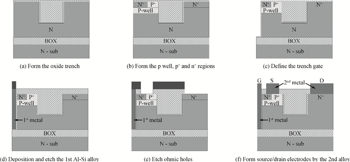
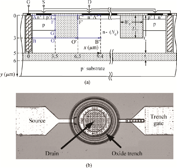
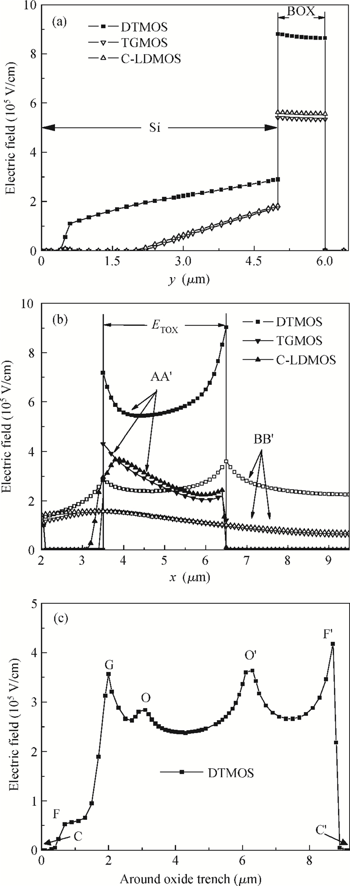
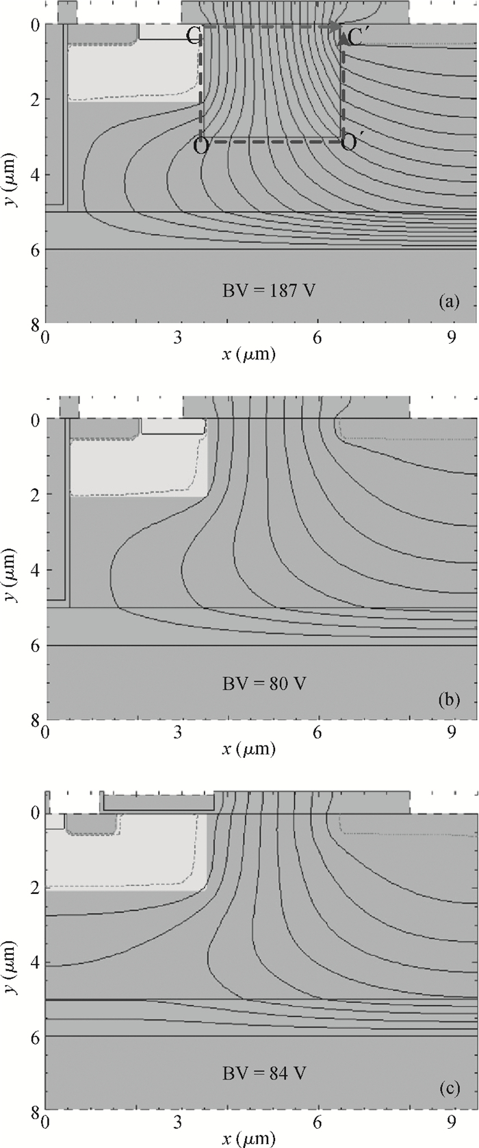
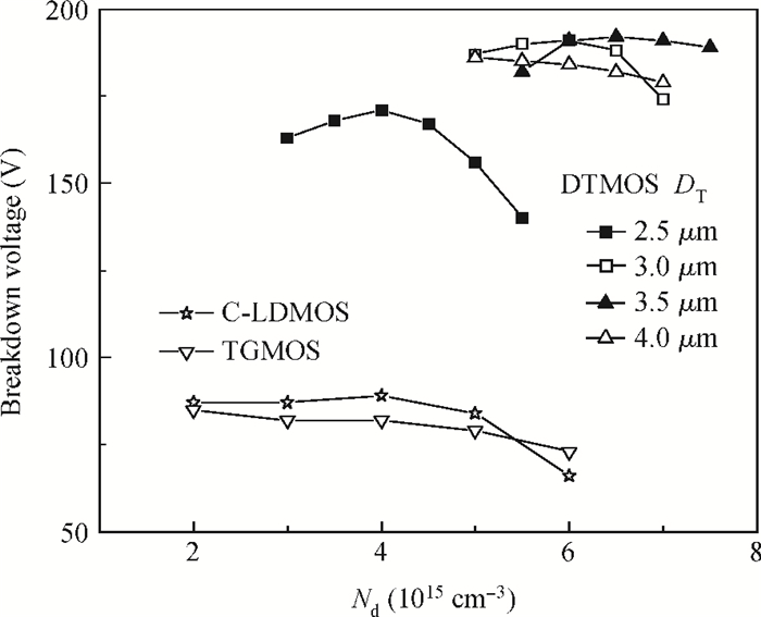
Abstract: An improved breakdown voltage (BV) SOI power MOSFET with a reduced cell pitch is proposed and fabricated. Its breakdown characteristics are investigated numerically and experimentally. The MOSFET features dual trenches (DTMOS), an oxide trench between the source and drain regions, and a trench gate extended to the buried oxide (BOX). The proposed device has three merits. First, the oxide trench increases the electric field strength in the x-direction due to the lower permittivity of oxide (εox) than that of Si (εSi). Furthermore, the trench gate, the oxide trench, and the BOX cause multi-directional depletion, improving the electric field distribution and enhancing the RESURF (reduced surface field) effect. Both increase the BV. Second, the oxide trench folds the drift region along the y-direction and thus reduces the cell pitch. Third, the trench gate not only reduces the on-resistance, but also acts as a field plate to improve the BV. Additionally, the trench gate achieves the isolation between high-voltage devices and the low voltage CMOS devices in a high-voltage integrated circuit (HVIC), effectively saving the chip area and simplifying the isolation process. An 180 V prototype DTMOS with its applied drive IC is fabricated to verify the mechanism.
Keywords: MOSFET, SOI, breakdown voltage, trench gate
| [1] |
Sona W S, Sohnb Y H, Choia S Y. RESURF LDMOSFET with a trench for SOI power integrated circuits. Microelectron J, 2004, 35(5):393 doi: 10.1016/j.mejo.2004.02.001
|
| [2] |
Fujishima N, Andre C, Salama T. A trench lateral power MOSFET using self-aligned trench bottom contact holes. IEDM Tech Dig, 1997:359 http://ieeexplore.ieee.org/document/650399/authors
|
| [3] |
Fujishima N, Sugi A, Andre C, et al. Method of manufacturing a semiconductor integrated circuit device. US Patent, No.7445983, 2008
|
| [4] |
Fujishima N, Sugi A, Andre C, et al. Trench-type MOSFET having a reduced device pitch and on-resistance. US Patent, No.7005352B2, 2006
|
| [5] |
Varadarajan K R, Chow T P, Wang J. 250 V integrable silicon lateral trench power MOSFETs with superior specific on-resistance. Proc ISPSD, 2007:233 http://ieeexplore.ieee.org/stamp/stamp.jsp?arnumber=4294975
|
| [6] |
Luo X, Zhang B, Li Z J. A new structure and its analytical model for the electric field and breakdown voltage of SOI high voltage device with variable-k dielectric buried layer. Solid State Electron, 2007, 51(3):493 doi: 10.1016/j.sse.2007.01.034
|
| [7] |
Luo X, Li Z J, Zhang B, et al. Realization of high voltage (≫700 V) in new SOI devices with a compound buried-layer. IEEE Electron Device Lett, 2008, 29(12):1395 doi: 10.1109/LED.2008.2007307
|
| [8] |
Luo X, Zhang B, Li Z J. A novel 700-V SOI LDMOS with double-sided trench. IEEE Electron Device Lett, 2007, 28(5):422 doi: 10.1109/LED.2007.894648
|


Article views: 3850 Times PDF downloads: 24 Times Cited by: 0 Times
Received: 12 July 2013 Revised: 07 August 2013 Online: Published: 01 February 2014
| Citation: |
Xiaorong Luo, Xiaowei Wang, Gangyi Hu, Yuanhang Fan, Kun Zhou, Yinchun Luo, Ye Fan, Zhengyuan Zhang, Yong Mei, Bo Zhang. Experimental and theoretical study of an improved breakdown voltage SOI LDMOS with a reduced cell pitch[J]. Journal of Semiconductors, 2014, 35(2): 024007. doi: 10.1088/1674-4926/35/2/024007
****
X R Luo, X W Wang, G Y Hu, Y H Fan, K Zhou, Y C Luo, Y Fan, Z Y Zhang, Y Mei, B Zhang. Experimental and theoretical study of an improved breakdown voltage SOI LDMOS with a reduced cell pitch[J]. J. Semicond., 2014, 35(2): 024007. doi: 10.1088/1674-4926/35/2/024007.

|
| [1] |
Sona W S, Sohnb Y H, Choia S Y. RESURF LDMOSFET with a trench for SOI power integrated circuits. Microelectron J, 2004, 35(5):393 doi: 10.1016/j.mejo.2004.02.001
|
| [2] |
Fujishima N, Andre C, Salama T. A trench lateral power MOSFET using self-aligned trench bottom contact holes. IEDM Tech Dig, 1997:359 http://ieeexplore.ieee.org/document/650399/authors
|
| [3] |
Fujishima N, Sugi A, Andre C, et al. Method of manufacturing a semiconductor integrated circuit device. US Patent, No.7445983, 2008
|
| [4] |
Fujishima N, Sugi A, Andre C, et al. Trench-type MOSFET having a reduced device pitch and on-resistance. US Patent, No.7005352B2, 2006
|
| [5] |
Varadarajan K R, Chow T P, Wang J. 250 V integrable silicon lateral trench power MOSFETs with superior specific on-resistance. Proc ISPSD, 2007:233 http://ieeexplore.ieee.org/stamp/stamp.jsp?arnumber=4294975
|
| [6] |
Luo X, Zhang B, Li Z J. A new structure and its analytical model for the electric field and breakdown voltage of SOI high voltage device with variable-k dielectric buried layer. Solid State Electron, 2007, 51(3):493 doi: 10.1016/j.sse.2007.01.034
|
| [7] |
Luo X, Li Z J, Zhang B, et al. Realization of high voltage (≫700 V) in new SOI devices with a compound buried-layer. IEEE Electron Device Lett, 2008, 29(12):1395 doi: 10.1109/LED.2008.2007307
|
| [8] |
Luo X, Zhang B, Li Z J. A novel 700-V SOI LDMOS with double-sided trench. IEEE Electron Device Lett, 2007, 28(5):422 doi: 10.1109/LED.2007.894648
|

 WeChat ID
Journal of Semiconductors © 2017 All Rights Reserved 京ICP备05085259号-2

 DownLoad: