


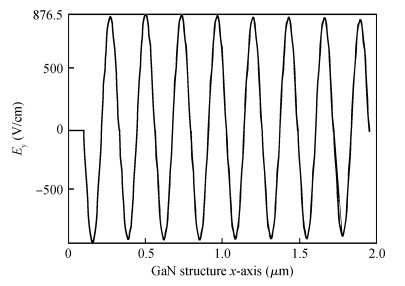
Fig. 1.
The transmitting electric fieldcomponent $E_{y}$ distribution of the light in GaN, the wavelength in the GaN is about 229 nm (550 nm in the air).
SEMICONDUCTOR MATERIALS
Linqing Li and Yanwu Lü
Corresponding author: Lü Yanwu, Email: ywlu@bjtu.edu.cn
Abstract: The transmitting light in GaN-based LED with 30 nm thickness metal film grating is investigated. We proposed a basic grating structure model to enhance light intensity in GaN material, which was simpler and cheaper. We calculated and analyzed the structure with different parameters, and studied the numerical simulation results of Ag-films/Al-films/Au-films. With a simple Al or Ag basic grating structure, the 7.4-7.6 times intensity of 550 nm light can be obtained easily, and the enhancement efficiency is better than others.
Keywords: GaN-based LED, surface plasmon, metal grating structure
| [1] |
Amano H, Sawaki N, Akasaki I, et al. Metal organic vapor phase epitaxial growth of a high quality GaN film using an AlN buffer layer. Appl Phys Lett, 1986, 8(5):353
|
| [2] |
Amano H, Kito M, Hiramatsu K, et al. P-type conduction in Mg-doped GaN treated with low-energy electron beam irradiation. Jpn J Appl Phys, 1989, 28:2112 doi: 10.1143/JJAP.28.L2112
|
| [3] |
Liang Chunguang, Zhang Ji. GaN dawn of 3rd generation semiconductors. Chinese Journal of Semiconductors, 1999, 20(2):89
|
| [4] |
Kaufmann U, Kunzer M, Köhler K, et al. Ultraviolet pumped tricolor phosphor blend white emitting LEDs. Phys Status Solidi A, 2001, 188:143 doi: 10.1002/(ISSN)1521-396X
|
| [5] |
Zou X, Wong K M, Zhu X, et al. High-performance green and yellow LEDs grown on SiO2 nanorod patterned GaN/Si templates. IEEE Electron Device Lett, 2013, 34(7):903 doi: 10.1109/LED.2013.2260126
|
| [6] |
Li Z, Waldron J, Detchprohm T, et al. Monolithic integration of light-emitting diodes and power metal-oxide-semiconductor channel high-electron-mobility transistors for light-emitting power integrated circuits in GaN on sapphire substrate. Appl Phys Lett, 2013, 102(19):192107 doi: 10.1063/1.4807125
|
| [7] |
Zhan Teng, Zhang Yang, Li Jing, et al. The design and fabrication of a GaN-based monolithic light-emitting diode array. Journal of Semiconductors, 2013, 34:094010 doi: 10.1088/1674-4926/34/9/094010
|
| [8] |
Nakamura S, Chichibu S F. Introduction to nitride semiconductor blue lasers and light emitting diodes. CRC Press, 2000
|
| [9] |
Yen S H, Tsai M C, Tsai M L, et al. Effect of N-type AlGaN layer on carrier transportation and efficiency droop of blue InGaN light-emitting diodes. IEEE Photonics Technol Lett, 2009, 21(14):975 doi: 10.1109/LPT.2009.2021155
|
| [10] |
Kuo Y K, Tsai M C, Yen S H, et al. Effect of P-type last barrier on efficiency droop of blue InGaN light-emitting diodes. IEEE J Quantum Electron, 2010, 46(8):1214
|
| [11] |
Fujii T, Gao Y, Sharma R, et al. Increase in the extraction efficiency of GaN-based light-emitting diodes via surface roughening. Appl Phys Lett, 2004, 84(6):855 doi: 10.1063/1.1645992
|
| [12] |
Kim D H, Cho C O, Roh Y G, et al. Enhanced light extraction from GaN-based light-emitting diodes with holographically generated two-dimensional photonic crystal patterns. Appl Phys Lett, 2005, 87(20):203508 doi: 10.1063/1.2132073
|
| [13] |
Xiao Gongli, Yang Hongyan. Significantly enhanced transmission achieved with double-layered metallic aperture arrays with sub-skin-depth Ag film. Journal of Semiconductors, 2012, 33(12):122001 doi: 10.1088/1674-4926/33/12/122001
|
| [14] |
Sung J H, Kim B S, Choi C H, et al. Enhanced luminescence of GaN-based light-emitting diode with a localized surface plasmon resonance. Microelectron Eng, 2009, 86:1120 doi: 10.1016/j.mee.2009.01.009
|
| [15] |
Zhang H, Zhu J, Zhu Z, et al. Surface-plasmon-enhanced GaN-LED based on a multilayered M-shaped nano-grating. Opt Express, 2013, 21(11):13492 doi: 10.1364/OE.21.013492
|
| [16] |
Ge D B, Yan Y B. Electromagnetic finite difference time domain method. Xi'an:Xi'an University of Electronic Science and Technology University Press, 2003(in Chinese)
|
| [17] |
Barnes W L, Dereux A, Ebbesen T W. Surface plasmon subwavelength optics. International Weekly Journal of Science, 2003, 424:824 http://www.nature.com/nature/journal/v424/n6950/full/nature01937.html
|
| [18] |
Bethe H A. Theory of diffraction by small holes. Phys Rev, 1944, 66(7/8):163
|
| [19] |
Forslund D W, Kindel J M, Lee K, et al. Theory and simulation of resonant absorption in a hot plasma. Phys Rev A, 1975, 11:679 doi: 10.1103/PhysRevA.11.679
|
| [20] |
Markovic M I, Rakic A D. Determination of reflection coefficients of laser light of wavelength λ ∈ (0.22μm, 200μm) from the surface of aluminum using the Lorentz-Drude model. Appl Opt, 1990, 29(24):3479 doi: 10.1364/AO.29.003479
|
| [21] |
Rakic A D, Djuriši A B, Elazar J M, et al. Optical properties of metallic films for vertical-cavity optoelectronic devices. Appl Opt, 1998, 37(22):5271 doi: 10.1364/AO.37.005271
|
| [22] |
Kretschmann E, Raether H. Radiative decay of non-radiative surface plasmon excited by light. Zeitschrift Fuer Naturforschung Teil A, 1968, 23A:2135
|
| [23] |
Wang T J, Tu C W, Liu F K, et al. Surface plasmon resonance waveguide biosensor by bipolarization wavelength interrogation. Photonic Technol Lett, 2004, 16(7):1715 doi: 10.1109/LPT.2004.828376
|
| [24] |
Hu C, Liu D. Polarization characteristics of subwavelength aluminum wire grating in near infrared. Research Article, 2009, 2(2):187 doi: 10.1007%2Fs12200-009-0027-7.pdf
|
| [25] |
Johnson P B, Christy R W. Optical constants of the noble metals. Phys Rev B, 1972, 6:4370 doi: 10.1103/PhysRevB.6.4370
|
| [26] |
Bohren C F, Huffman D R. Absorption and scattering of light by small particles. New York:A Wiley Interscience Publication, 1983
|
| [27] |
Hu Changkui. Study on surface plasmon resonance sensor based on nano metallic surface-relief gratings. The Huazhong University of Science and Technology (HUST), 2010
|
| [28] |
Raether H. Surface plasmons on smooth and rough surfaces and on gratings. Springer Tracts in Modern Physics, 1988, 111:4 doi: 10.1007/BFb0048317
|
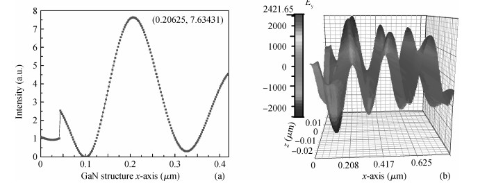
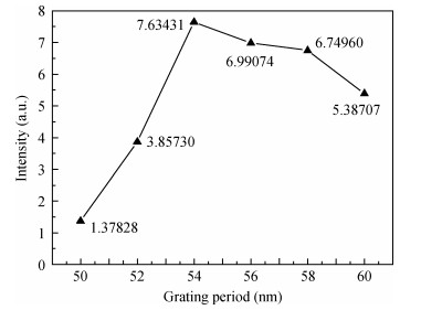
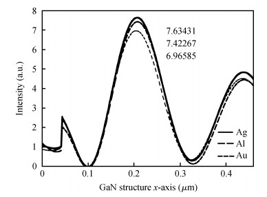
Table 1. Parameters of silver in angle frequency unit (Rad/s).

|
| [1] |
Amano H, Sawaki N, Akasaki I, et al. Metal organic vapor phase epitaxial growth of a high quality GaN film using an AlN buffer layer. Appl Phys Lett, 1986, 8(5):353
|
| [2] |
Amano H, Kito M, Hiramatsu K, et al. P-type conduction in Mg-doped GaN treated with low-energy electron beam irradiation. Jpn J Appl Phys, 1989, 28:2112 doi: 10.1143/JJAP.28.L2112
|
| [3] |
Liang Chunguang, Zhang Ji. GaN dawn of 3rd generation semiconductors. Chinese Journal of Semiconductors, 1999, 20(2):89
|
| [4] |
Kaufmann U, Kunzer M, Köhler K, et al. Ultraviolet pumped tricolor phosphor blend white emitting LEDs. Phys Status Solidi A, 2001, 188:143 doi: 10.1002/(ISSN)1521-396X
|
| [5] |
Zou X, Wong K M, Zhu X, et al. High-performance green and yellow LEDs grown on SiO2 nanorod patterned GaN/Si templates. IEEE Electron Device Lett, 2013, 34(7):903 doi: 10.1109/LED.2013.2260126
|
| [6] |
Li Z, Waldron J, Detchprohm T, et al. Monolithic integration of light-emitting diodes and power metal-oxide-semiconductor channel high-electron-mobility transistors for light-emitting power integrated circuits in GaN on sapphire substrate. Appl Phys Lett, 2013, 102(19):192107 doi: 10.1063/1.4807125
|
| [7] |
Zhan Teng, Zhang Yang, Li Jing, et al. The design and fabrication of a GaN-based monolithic light-emitting diode array. Journal of Semiconductors, 2013, 34:094010 doi: 10.1088/1674-4926/34/9/094010
|
| [8] |
Nakamura S, Chichibu S F. Introduction to nitride semiconductor blue lasers and light emitting diodes. CRC Press, 2000
|
| [9] |
Yen S H, Tsai M C, Tsai M L, et al. Effect of N-type AlGaN layer on carrier transportation and efficiency droop of blue InGaN light-emitting diodes. IEEE Photonics Technol Lett, 2009, 21(14):975 doi: 10.1109/LPT.2009.2021155
|
| [10] |
Kuo Y K, Tsai M C, Yen S H, et al. Effect of P-type last barrier on efficiency droop of blue InGaN light-emitting diodes. IEEE J Quantum Electron, 2010, 46(8):1214
|
| [11] |
Fujii T, Gao Y, Sharma R, et al. Increase in the extraction efficiency of GaN-based light-emitting diodes via surface roughening. Appl Phys Lett, 2004, 84(6):855 doi: 10.1063/1.1645992
|
| [12] |
Kim D H, Cho C O, Roh Y G, et al. Enhanced light extraction from GaN-based light-emitting diodes with holographically generated two-dimensional photonic crystal patterns. Appl Phys Lett, 2005, 87(20):203508 doi: 10.1063/1.2132073
|
| [13] |
Xiao Gongli, Yang Hongyan. Significantly enhanced transmission achieved with double-layered metallic aperture arrays with sub-skin-depth Ag film. Journal of Semiconductors, 2012, 33(12):122001 doi: 10.1088/1674-4926/33/12/122001
|
| [14] |
Sung J H, Kim B S, Choi C H, et al. Enhanced luminescence of GaN-based light-emitting diode with a localized surface plasmon resonance. Microelectron Eng, 2009, 86:1120 doi: 10.1016/j.mee.2009.01.009
|
| [15] |
Zhang H, Zhu J, Zhu Z, et al. Surface-plasmon-enhanced GaN-LED based on a multilayered M-shaped nano-grating. Opt Express, 2013, 21(11):13492 doi: 10.1364/OE.21.013492
|
| [16] |
Ge D B, Yan Y B. Electromagnetic finite difference time domain method. Xi'an:Xi'an University of Electronic Science and Technology University Press, 2003(in Chinese)
|
| [17] |
Barnes W L, Dereux A, Ebbesen T W. Surface plasmon subwavelength optics. International Weekly Journal of Science, 2003, 424:824 http://www.nature.com/nature/journal/v424/n6950/full/nature01937.html
|
| [18] |
Bethe H A. Theory of diffraction by small holes. Phys Rev, 1944, 66(7/8):163
|
| [19] |
Forslund D W, Kindel J M, Lee K, et al. Theory and simulation of resonant absorption in a hot plasma. Phys Rev A, 1975, 11:679 doi: 10.1103/PhysRevA.11.679
|
| [20] |
Markovic M I, Rakic A D. Determination of reflection coefficients of laser light of wavelength λ ∈ (0.22μm, 200μm) from the surface of aluminum using the Lorentz-Drude model. Appl Opt, 1990, 29(24):3479 doi: 10.1364/AO.29.003479
|
| [21] |
Rakic A D, Djuriši A B, Elazar J M, et al. Optical properties of metallic films for vertical-cavity optoelectronic devices. Appl Opt, 1998, 37(22):5271 doi: 10.1364/AO.37.005271
|
| [22] |
Kretschmann E, Raether H. Radiative decay of non-radiative surface plasmon excited by light. Zeitschrift Fuer Naturforschung Teil A, 1968, 23A:2135
|
| [23] |
Wang T J, Tu C W, Liu F K, et al. Surface plasmon resonance waveguide biosensor by bipolarization wavelength interrogation. Photonic Technol Lett, 2004, 16(7):1715 doi: 10.1109/LPT.2004.828376
|
| [24] |
Hu C, Liu D. Polarization characteristics of subwavelength aluminum wire grating in near infrared. Research Article, 2009, 2(2):187 doi: 10.1007%2Fs12200-009-0027-7.pdf
|
| [25] |
Johnson P B, Christy R W. Optical constants of the noble metals. Phys Rev B, 1972, 6:4370 doi: 10.1103/PhysRevB.6.4370
|
| [26] |
Bohren C F, Huffman D R. Absorption and scattering of light by small particles. New York:A Wiley Interscience Publication, 1983
|
| [27] |
Hu Changkui. Study on surface plasmon resonance sensor based on nano metallic surface-relief gratings. The Huazhong University of Science and Technology (HUST), 2010
|
| [28] |
Raether H. Surface plasmons on smooth and rough surfaces and on gratings. Springer Tracts in Modern Physics, 1988, 111:4 doi: 10.1007/BFb0048317
|


Article views: 3118 Times PDF downloads: 7 Times Cited by: 0 Times
Received: 06 September 2013 Revised: 14 November 2013 Online: Published: 01 April 2014
| Citation: |
Linqing Li, Yanwu Lü. Surface-plasmon-enhanced light transmission intensity with a basic grating in GaN-based LED[J]. Journal of Semiconductors, 2014, 35(4): 043003. doi: 10.1088/1674-4926/35/4/043003
****
L Q Li, Y Lü. Surface-plasmon-enhanced light transmission intensity with a basic grating in GaN-based LED[J]. J. Semicond., 2014, 35(4): 043003. doi: 10.1088/1674-4926/35/4/043003.

|
| [1] |
Amano H, Sawaki N, Akasaki I, et al. Metal organic vapor phase epitaxial growth of a high quality GaN film using an AlN buffer layer. Appl Phys Lett, 1986, 8(5):353
|
| [2] |
Amano H, Kito M, Hiramatsu K, et al. P-type conduction in Mg-doped GaN treated with low-energy electron beam irradiation. Jpn J Appl Phys, 1989, 28:2112 doi: 10.1143/JJAP.28.L2112
|
| [3] |
Liang Chunguang, Zhang Ji. GaN dawn of 3rd generation semiconductors. Chinese Journal of Semiconductors, 1999, 20(2):89
|
| [4] |
Kaufmann U, Kunzer M, Köhler K, et al. Ultraviolet pumped tricolor phosphor blend white emitting LEDs. Phys Status Solidi A, 2001, 188:143 doi: 10.1002/(ISSN)1521-396X
|
| [5] |
Zou X, Wong K M, Zhu X, et al. High-performance green and yellow LEDs grown on SiO2 nanorod patterned GaN/Si templates. IEEE Electron Device Lett, 2013, 34(7):903 doi: 10.1109/LED.2013.2260126
|
| [6] |
Li Z, Waldron J, Detchprohm T, et al. Monolithic integration of light-emitting diodes and power metal-oxide-semiconductor channel high-electron-mobility transistors for light-emitting power integrated circuits in GaN on sapphire substrate. Appl Phys Lett, 2013, 102(19):192107 doi: 10.1063/1.4807125
|
| [7] |
Zhan Teng, Zhang Yang, Li Jing, et al. The design and fabrication of a GaN-based monolithic light-emitting diode array. Journal of Semiconductors, 2013, 34:094010 doi: 10.1088/1674-4926/34/9/094010
|
| [8] |
Nakamura S, Chichibu S F. Introduction to nitride semiconductor blue lasers and light emitting diodes. CRC Press, 2000
|
| [9] |
Yen S H, Tsai M C, Tsai M L, et al. Effect of N-type AlGaN layer on carrier transportation and efficiency droop of blue InGaN light-emitting diodes. IEEE Photonics Technol Lett, 2009, 21(14):975 doi: 10.1109/LPT.2009.2021155
|
| [10] |
Kuo Y K, Tsai M C, Yen S H, et al. Effect of P-type last barrier on efficiency droop of blue InGaN light-emitting diodes. IEEE J Quantum Electron, 2010, 46(8):1214
|
| [11] |
Fujii T, Gao Y, Sharma R, et al. Increase in the extraction efficiency of GaN-based light-emitting diodes via surface roughening. Appl Phys Lett, 2004, 84(6):855 doi: 10.1063/1.1645992
|
| [12] |
Kim D H, Cho C O, Roh Y G, et al. Enhanced light extraction from GaN-based light-emitting diodes with holographically generated two-dimensional photonic crystal patterns. Appl Phys Lett, 2005, 87(20):203508 doi: 10.1063/1.2132073
|
| [13] |
Xiao Gongli, Yang Hongyan. Significantly enhanced transmission achieved with double-layered metallic aperture arrays with sub-skin-depth Ag film. Journal of Semiconductors, 2012, 33(12):122001 doi: 10.1088/1674-4926/33/12/122001
|
| [14] |
Sung J H, Kim B S, Choi C H, et al. Enhanced luminescence of GaN-based light-emitting diode with a localized surface plasmon resonance. Microelectron Eng, 2009, 86:1120 doi: 10.1016/j.mee.2009.01.009
|
| [15] |
Zhang H, Zhu J, Zhu Z, et al. Surface-plasmon-enhanced GaN-LED based on a multilayered M-shaped nano-grating. Opt Express, 2013, 21(11):13492 doi: 10.1364/OE.21.013492
|
| [16] |
Ge D B, Yan Y B. Electromagnetic finite difference time domain method. Xi'an:Xi'an University of Electronic Science and Technology University Press, 2003(in Chinese)
|
| [17] |
Barnes W L, Dereux A, Ebbesen T W. Surface plasmon subwavelength optics. International Weekly Journal of Science, 2003, 424:824 http://www.nature.com/nature/journal/v424/n6950/full/nature01937.html
|
| [18] |
Bethe H A. Theory of diffraction by small holes. Phys Rev, 1944, 66(7/8):163
|
| [19] |
Forslund D W, Kindel J M, Lee K, et al. Theory and simulation of resonant absorption in a hot plasma. Phys Rev A, 1975, 11:679 doi: 10.1103/PhysRevA.11.679
|
| [20] |
Markovic M I, Rakic A D. Determination of reflection coefficients of laser light of wavelength λ ∈ (0.22μm, 200μm) from the surface of aluminum using the Lorentz-Drude model. Appl Opt, 1990, 29(24):3479 doi: 10.1364/AO.29.003479
|
| [21] |
Rakic A D, Djuriši A B, Elazar J M, et al. Optical properties of metallic films for vertical-cavity optoelectronic devices. Appl Opt, 1998, 37(22):5271 doi: 10.1364/AO.37.005271
|
| [22] |
Kretschmann E, Raether H. Radiative decay of non-radiative surface plasmon excited by light. Zeitschrift Fuer Naturforschung Teil A, 1968, 23A:2135
|
| [23] |
Wang T J, Tu C W, Liu F K, et al. Surface plasmon resonance waveguide biosensor by bipolarization wavelength interrogation. Photonic Technol Lett, 2004, 16(7):1715 doi: 10.1109/LPT.2004.828376
|
| [24] |
Hu C, Liu D. Polarization characteristics of subwavelength aluminum wire grating in near infrared. Research Article, 2009, 2(2):187 doi: 10.1007%2Fs12200-009-0027-7.pdf
|
| [25] |
Johnson P B, Christy R W. Optical constants of the noble metals. Phys Rev B, 1972, 6:4370 doi: 10.1103/PhysRevB.6.4370
|
| [26] |
Bohren C F, Huffman D R. Absorption and scattering of light by small particles. New York:A Wiley Interscience Publication, 1983
|
| [27] |
Hu Changkui. Study on surface plasmon resonance sensor based on nano metallic surface-relief gratings. The Huazhong University of Science and Technology (HUST), 2010
|
| [28] |
Raether H. Surface plasmons on smooth and rough surfaces and on gratings. Springer Tracts in Modern Physics, 1988, 111:4 doi: 10.1007/BFb0048317
|

 WeChat ID
Journal of Semiconductors © 2017 All Rights Reserved 京ICP备05085259号-2

 DownLoad:

