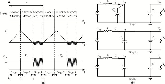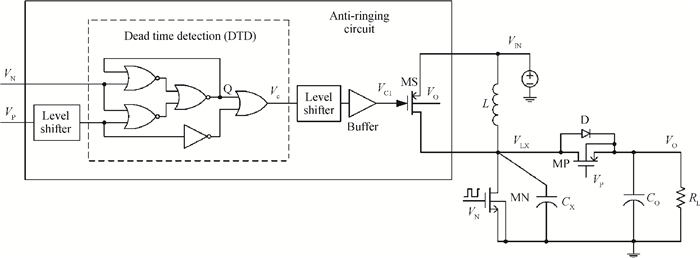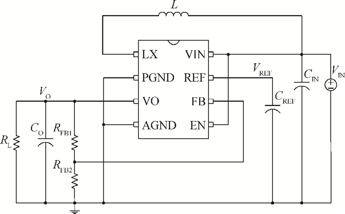
Fig. 1.
Schematic of a conventional synchronous boost DC-DC converter.
SEMICONDUCTOR INTEGRATED CIRCUITS
Yajun Li1, , Xinquan Lai1, Qiang Ye2 and Bing Yuan2
Corresponding author: Li Yajun, Email:yajunli@stu.xidian.edu.cn
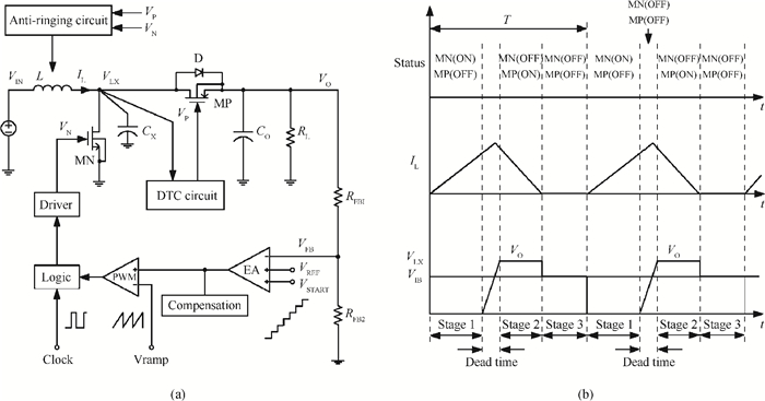
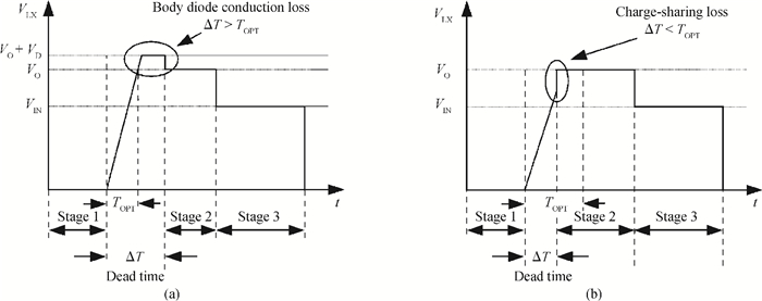
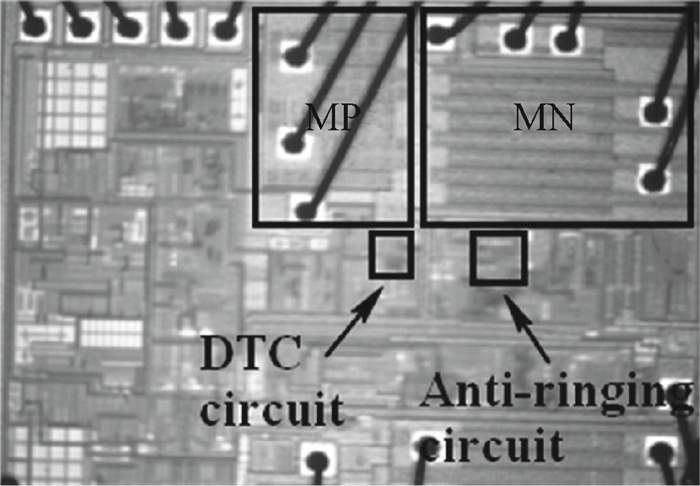
Abstract: A synchronous boost DC-DC converter with an adaptive dead time control (DTC) circuit and anti-ringing circuit is presented. The DTC circuit is used to provide adjustable dead time and zero inductor current detection for power transistors and therefore, a high efficiency is achieved by minimizing power losses, such as the shoot-through current loss, the body diode conduction loss, the charge-sharing loss and the reverse inductor current loss. Simultaneously, a novel anti-ringing circuit controlled by the switching sequence of power transistors is developed to suppress the ringing when the converter enters the discontinuous conduction mode (DCM) for low electromagnetic interference (EMI) and additional power savings. The proposed converter has been fabricated in a 0.6 μm CDMOS technology. Simulation and experimental results show that the power efficiency of the boost converter is above 81% under different load currents from 10 to 250 mA and a peak efficiency of 90% is achieved at about 100 mA. Moreover, the ringing is easily suppressed by the anti-ringing circuit and therefore the EMI noise is attenuated.
Keywords: DC-DC, dead time, discontinuous conduction mode, electromagnetic interference, anti-ringing
| [1] |
Ye Qiang, Lai Xinquan, Li Yanming, et al. A piecewise linear slope compensation circuit for DC-DC converters. Journal of Semiconductors, 2008, 29(2):281 http://www.jos.ac.cn/bdtxbcn/ch/reader/view_abstract.aspx?file_no=07080602&flag=1
|
| [2] |
Chen Fuji, Lai Xinquan, Li Yushan. Design and implementation of an adaptive slope compensation circuit. Journal of Semiconductors, 2008, 29(3):593 http://www.jos.ac.cn/bdtxbcn/ch/reader/view_abstract.aspx?file_no=07061101&flag=1
|
| [3] |
Chen Fuji, Lai Xinquan, Li Yushan, et al. Design of a low input voltage startup circuit for the boost DC-DC converter. Journal of Xidian University, 2010, 37(3):476 http://en.cnki.com.cn/Article_en/CJFDTOTAL-XDKD201003017.htm
|
| [4] |
Lai Xinquan, Zeng Huali, Ye Qiang, et al. Design of high efficiency dual-mode buck DC-DC converter. Journal of Semiconductors, 2010, 31(11):115005 doi: 10.1088/1674-4926/31/11/115005
|
| [5] |
Yuan Bing, Lai Xinquan, Li Yanming, et al. High efficiency realization of a DC-DC converter at light loads for portable applications. Journal of Semiconductors, 2008, 29(6):1198 http://www.jos.ac.cn/bdtxbcn/ch/reader/view_abstract.aspx?file_no=07102205&flag=1
|
| [6] |
Li Yanming, Lai Xinquan, Yuan Bing, et al. An on-chip soft-start circuit for DC-DC switching regulators. Journal of Semiconductors, 2008, 29(6):1210 http://www.jos.ac.cn/bdtxbcn/ch/reader/view_abstract.aspx?file_no=07110601&flag=1
|
| [7] |
Liu Y X, Liu S B, Li Y M, et al. Design and implementation of a compact frequency synchronisation control circuit using enable input for DC-DC converter. IET Power Electron, 2012, 5(9):1827 doi: 10.1049/iet-pel.2012.0187
|
| [8] |
Hamza D, Sawan M, Jain P K. Suppression of common-mode input electromagnetic interference noise in DC-DC converters using the active filtering method. IET Power Electron, 2011, 4(7):776 doi: 10.1049/iet-pel.2010.0200
|
| [9] |
Chen Wenjie, Yang Xu, Wang Zhaoan. An active EMI filtering technique for improving passive filter low-frequency performance. IEEE Trans EMC, 2006, 48(1):172 http://ieeexplore.ieee.org/document/1614050/
|
| [10] |
Wang Hongyi, Lai Xinquan, Li Yushan, et al. A novel anti-ringing circuit for buck DC-DC chip. Acta Electronica Sinica, 2006, 34(2):361 http://en.cnki.com.cn/Article_en/CJFDTotal-DZXU200602031.htm
|
| [11] |
Wang N, O'Donnell T, Meere R, et al. Thin-film-integrated power inductor on Si and its performance in an 8-MHz buck converter. IEEE Trans Magn, 2008, 44(11):4096 doi: 10.1109/TMAG.2008.2001584
|
| [12] |
Du M, Lee H, Liu J. A 5-MHz 91% peak-power-efficiency buck regulator with auto-selectable peak-and valley-current control. IEEE J Solid-State Circuits, 2011, 46(8):1928 doi: 10.1109/JSSC.2011.2151470
|
| [13] |
Wibben J, Harjani R. A high-efficiency DC-DC converter using 2 nH integrated inductors. IEEE J Solid-State Circuits, 2008, 43(4):844 doi: 10.1109/JSSC.2008.917321
|
| [14] |
Ye Qiang, Liu Jie, Yuan Bing, et al. On-chip frequency compensation with a dual signal path operational transconductance amplifier for a voltage mode control DC/DC converter. Journal of Semiconductors, 2012, 33(4):045006 doi: 10.1088/1674-4926/33/4/045006
|
| [15] |
Lai Xinquan, Li Zuhe, Yuan Bing, et al. Control of chaos in double-loop current-mode DC/DC based on adaptive slope compensation. Acta Physica Sinica, 2010, 59(4):2256 http://en.cnki.com.cn/Article_en/CJFDTOTAL-WLXB201004016.htm
|
| [16] |
Yuan Bing, Lai Xinquan, Ye Qiang, et al. An integrated current-sensing circuit for current-mode DC-DC buck converters. Journal of Semiconductors, 2008, 29(8):1627 http://www.jos.ac.cn/bdtxbcn/ch/reader/view_abstract.aspx?file_no=08011303&flag=1
|
| [17] |
Yuan Bing, Lai Xinquan, Jia Xinzhang, et al. Implementation of high stability with on-chip frequency compensation in a current mode DC-DC converter. Journal of Xidian University, 2008, 35(4):685 http://en.cnki.com.cn/Article_en/CJFDTOTAL-XDKD200804019.htm
|
| [18] |
Lee C F, Mok P K T. A monolithic current-mode CMOS DC-DC converter with on-chip current-sensing technique. IEEE J Solid-State Circuits, 2004, 39(1):3 http://ieeexplore.ieee.org/document/1261283/
|
| [19] |
Yousefzadeh V, Maksimovi D. Sensorless optimization of dead times in DC-DC converters with synchronous rectifiers. IEEE Trans Power Electron, 2006, 21(4):994 doi: 10.1109/TPEL.2006.876850
|
| [20] |
Reiter T, Polenov D, Pröbstle H, et al. PWM dead time optimization method for automotive multiphase DC/DC-converters. IEEE Trans Power Electron, 2010, 25(6):1604 doi: 10.1109/TPEL.2009.2038379
|
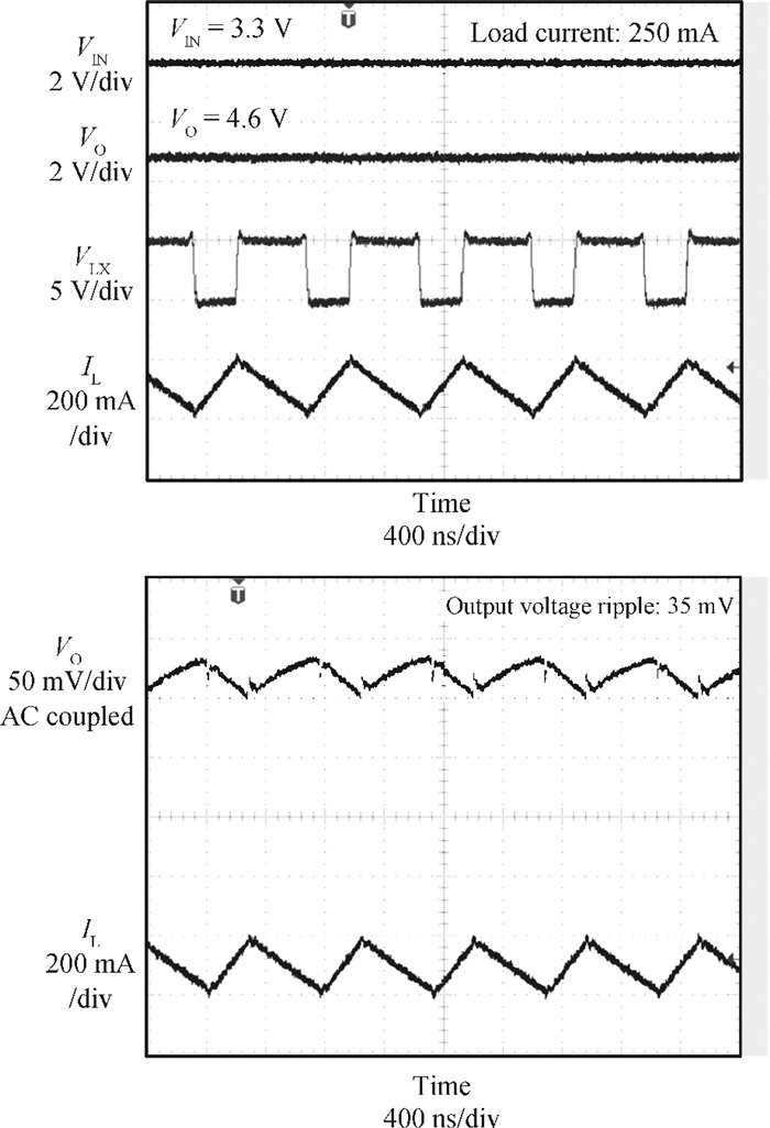
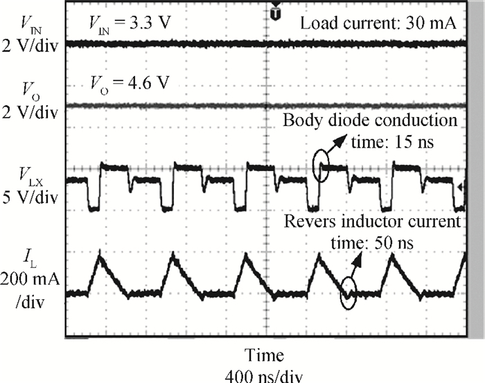
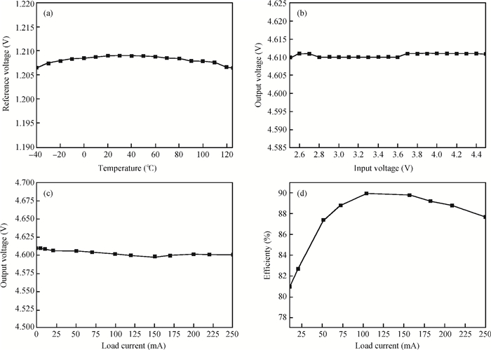
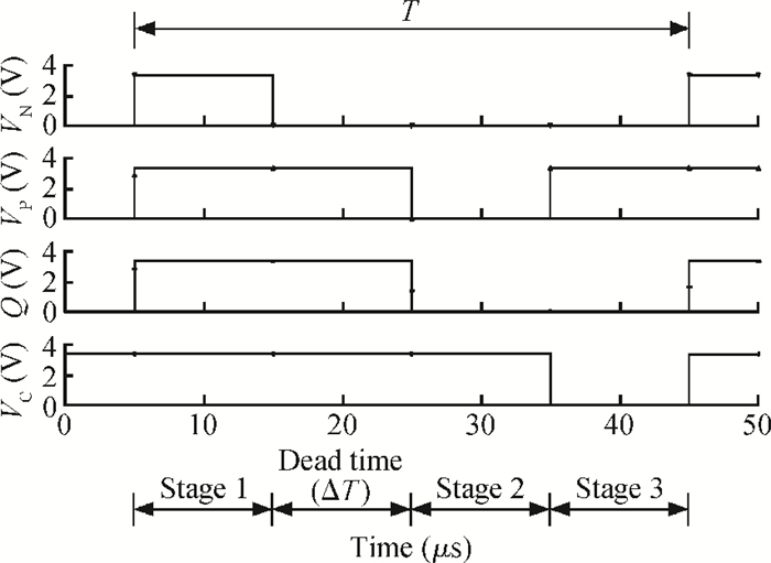
Table 1. State transition table of the proposed DTD circuit.

|
Table 2. Component values and output voltage

|
Table 3. Performance comparison summary of the chips.

|
| [1] |
Ye Qiang, Lai Xinquan, Li Yanming, et al. A piecewise linear slope compensation circuit for DC-DC converters. Journal of Semiconductors, 2008, 29(2):281 http://www.jos.ac.cn/bdtxbcn/ch/reader/view_abstract.aspx?file_no=07080602&flag=1
|
| [2] |
Chen Fuji, Lai Xinquan, Li Yushan. Design and implementation of an adaptive slope compensation circuit. Journal of Semiconductors, 2008, 29(3):593 http://www.jos.ac.cn/bdtxbcn/ch/reader/view_abstract.aspx?file_no=07061101&flag=1
|
| [3] |
Chen Fuji, Lai Xinquan, Li Yushan, et al. Design of a low input voltage startup circuit for the boost DC-DC converter. Journal of Xidian University, 2010, 37(3):476 http://en.cnki.com.cn/Article_en/CJFDTOTAL-XDKD201003017.htm
|
| [4] |
Lai Xinquan, Zeng Huali, Ye Qiang, et al. Design of high efficiency dual-mode buck DC-DC converter. Journal of Semiconductors, 2010, 31(11):115005 doi: 10.1088/1674-4926/31/11/115005
|
| [5] |
Yuan Bing, Lai Xinquan, Li Yanming, et al. High efficiency realization of a DC-DC converter at light loads for portable applications. Journal of Semiconductors, 2008, 29(6):1198 http://www.jos.ac.cn/bdtxbcn/ch/reader/view_abstract.aspx?file_no=07102205&flag=1
|
| [6] |
Li Yanming, Lai Xinquan, Yuan Bing, et al. An on-chip soft-start circuit for DC-DC switching regulators. Journal of Semiconductors, 2008, 29(6):1210 http://www.jos.ac.cn/bdtxbcn/ch/reader/view_abstract.aspx?file_no=07110601&flag=1
|
| [7] |
Liu Y X, Liu S B, Li Y M, et al. Design and implementation of a compact frequency synchronisation control circuit using enable input for DC-DC converter. IET Power Electron, 2012, 5(9):1827 doi: 10.1049/iet-pel.2012.0187
|
| [8] |
Hamza D, Sawan M, Jain P K. Suppression of common-mode input electromagnetic interference noise in DC-DC converters using the active filtering method. IET Power Electron, 2011, 4(7):776 doi: 10.1049/iet-pel.2010.0200
|
| [9] |
Chen Wenjie, Yang Xu, Wang Zhaoan. An active EMI filtering technique for improving passive filter low-frequency performance. IEEE Trans EMC, 2006, 48(1):172 http://ieeexplore.ieee.org/document/1614050/
|
| [10] |
Wang Hongyi, Lai Xinquan, Li Yushan, et al. A novel anti-ringing circuit for buck DC-DC chip. Acta Electronica Sinica, 2006, 34(2):361 http://en.cnki.com.cn/Article_en/CJFDTotal-DZXU200602031.htm
|
| [11] |
Wang N, O'Donnell T, Meere R, et al. Thin-film-integrated power inductor on Si and its performance in an 8-MHz buck converter. IEEE Trans Magn, 2008, 44(11):4096 doi: 10.1109/TMAG.2008.2001584
|
| [12] |
Du M, Lee H, Liu J. A 5-MHz 91% peak-power-efficiency buck regulator with auto-selectable peak-and valley-current control. IEEE J Solid-State Circuits, 2011, 46(8):1928 doi: 10.1109/JSSC.2011.2151470
|
| [13] |
Wibben J, Harjani R. A high-efficiency DC-DC converter using 2 nH integrated inductors. IEEE J Solid-State Circuits, 2008, 43(4):844 doi: 10.1109/JSSC.2008.917321
|
| [14] |
Ye Qiang, Liu Jie, Yuan Bing, et al. On-chip frequency compensation with a dual signal path operational transconductance amplifier for a voltage mode control DC/DC converter. Journal of Semiconductors, 2012, 33(4):045006 doi: 10.1088/1674-4926/33/4/045006
|
| [15] |
Lai Xinquan, Li Zuhe, Yuan Bing, et al. Control of chaos in double-loop current-mode DC/DC based on adaptive slope compensation. Acta Physica Sinica, 2010, 59(4):2256 http://en.cnki.com.cn/Article_en/CJFDTOTAL-WLXB201004016.htm
|
| [16] |
Yuan Bing, Lai Xinquan, Ye Qiang, et al. An integrated current-sensing circuit for current-mode DC-DC buck converters. Journal of Semiconductors, 2008, 29(8):1627 http://www.jos.ac.cn/bdtxbcn/ch/reader/view_abstract.aspx?file_no=08011303&flag=1
|
| [17] |
Yuan Bing, Lai Xinquan, Jia Xinzhang, et al. Implementation of high stability with on-chip frequency compensation in a current mode DC-DC converter. Journal of Xidian University, 2008, 35(4):685 http://en.cnki.com.cn/Article_en/CJFDTOTAL-XDKD200804019.htm
|
| [18] |
Lee C F, Mok P K T. A monolithic current-mode CMOS DC-DC converter with on-chip current-sensing technique. IEEE J Solid-State Circuits, 2004, 39(1):3 http://ieeexplore.ieee.org/document/1261283/
|
| [19] |
Yousefzadeh V, Maksimovi D. Sensorless optimization of dead times in DC-DC converters with synchronous rectifiers. IEEE Trans Power Electron, 2006, 21(4):994 doi: 10.1109/TPEL.2006.876850
|
| [20] |
Reiter T, Polenov D, Pröbstle H, et al. PWM dead time optimization method for automotive multiphase DC/DC-converters. IEEE Trans Power Electron, 2010, 25(6):1604 doi: 10.1109/TPEL.2009.2038379
|


Article views: 3971 Times PDF downloads: 134 Times Cited by: 0 Times
Received: 27 July 2013 Revised: 09 November 2013 Online: Published: 01 April 2014
| Citation: |
Yajun Li, Xinquan Lai, Qiang Ye, Bing Yuan. High efficiency and low electromagnetic interference boost DC-DC converter[J]. Journal of Semiconductors, 2014, 35(4): 045002. doi: 10.1088/1674-4926/35/4/045002
****
Y J Li, X Q Lai, Q Ye, B Yuan. High efficiency and low electromagnetic interference boost DC-DC converter[J]. J. Semicond., 2014, 35(4): 045002. doi: 10.1088/1674-4926/35/4/045002.

|
| [1] |
Ye Qiang, Lai Xinquan, Li Yanming, et al. A piecewise linear slope compensation circuit for DC-DC converters. Journal of Semiconductors, 2008, 29(2):281 http://www.jos.ac.cn/bdtxbcn/ch/reader/view_abstract.aspx?file_no=07080602&flag=1
|
| [2] |
Chen Fuji, Lai Xinquan, Li Yushan. Design and implementation of an adaptive slope compensation circuit. Journal of Semiconductors, 2008, 29(3):593 http://www.jos.ac.cn/bdtxbcn/ch/reader/view_abstract.aspx?file_no=07061101&flag=1
|
| [3] |
Chen Fuji, Lai Xinquan, Li Yushan, et al. Design of a low input voltage startup circuit for the boost DC-DC converter. Journal of Xidian University, 2010, 37(3):476 http://en.cnki.com.cn/Article_en/CJFDTOTAL-XDKD201003017.htm
|
| [4] |
Lai Xinquan, Zeng Huali, Ye Qiang, et al. Design of high efficiency dual-mode buck DC-DC converter. Journal of Semiconductors, 2010, 31(11):115005 doi: 10.1088/1674-4926/31/11/115005
|
| [5] |
Yuan Bing, Lai Xinquan, Li Yanming, et al. High efficiency realization of a DC-DC converter at light loads for portable applications. Journal of Semiconductors, 2008, 29(6):1198 http://www.jos.ac.cn/bdtxbcn/ch/reader/view_abstract.aspx?file_no=07102205&flag=1
|
| [6] |
Li Yanming, Lai Xinquan, Yuan Bing, et al. An on-chip soft-start circuit for DC-DC switching regulators. Journal of Semiconductors, 2008, 29(6):1210 http://www.jos.ac.cn/bdtxbcn/ch/reader/view_abstract.aspx?file_no=07110601&flag=1
|
| [7] |
Liu Y X, Liu S B, Li Y M, et al. Design and implementation of a compact frequency synchronisation control circuit using enable input for DC-DC converter. IET Power Electron, 2012, 5(9):1827 doi: 10.1049/iet-pel.2012.0187
|
| [8] |
Hamza D, Sawan M, Jain P K. Suppression of common-mode input electromagnetic interference noise in DC-DC converters using the active filtering method. IET Power Electron, 2011, 4(7):776 doi: 10.1049/iet-pel.2010.0200
|
| [9] |
Chen Wenjie, Yang Xu, Wang Zhaoan. An active EMI filtering technique for improving passive filter low-frequency performance. IEEE Trans EMC, 2006, 48(1):172 http://ieeexplore.ieee.org/document/1614050/
|
| [10] |
Wang Hongyi, Lai Xinquan, Li Yushan, et al. A novel anti-ringing circuit for buck DC-DC chip. Acta Electronica Sinica, 2006, 34(2):361 http://en.cnki.com.cn/Article_en/CJFDTotal-DZXU200602031.htm
|
| [11] |
Wang N, O'Donnell T, Meere R, et al. Thin-film-integrated power inductor on Si and its performance in an 8-MHz buck converter. IEEE Trans Magn, 2008, 44(11):4096 doi: 10.1109/TMAG.2008.2001584
|
| [12] |
Du M, Lee H, Liu J. A 5-MHz 91% peak-power-efficiency buck regulator with auto-selectable peak-and valley-current control. IEEE J Solid-State Circuits, 2011, 46(8):1928 doi: 10.1109/JSSC.2011.2151470
|
| [13] |
Wibben J, Harjani R. A high-efficiency DC-DC converter using 2 nH integrated inductors. IEEE J Solid-State Circuits, 2008, 43(4):844 doi: 10.1109/JSSC.2008.917321
|
| [14] |
Ye Qiang, Liu Jie, Yuan Bing, et al. On-chip frequency compensation with a dual signal path operational transconductance amplifier for a voltage mode control DC/DC converter. Journal of Semiconductors, 2012, 33(4):045006 doi: 10.1088/1674-4926/33/4/045006
|
| [15] |
Lai Xinquan, Li Zuhe, Yuan Bing, et al. Control of chaos in double-loop current-mode DC/DC based on adaptive slope compensation. Acta Physica Sinica, 2010, 59(4):2256 http://en.cnki.com.cn/Article_en/CJFDTOTAL-WLXB201004016.htm
|
| [16] |
Yuan Bing, Lai Xinquan, Ye Qiang, et al. An integrated current-sensing circuit for current-mode DC-DC buck converters. Journal of Semiconductors, 2008, 29(8):1627 http://www.jos.ac.cn/bdtxbcn/ch/reader/view_abstract.aspx?file_no=08011303&flag=1
|
| [17] |
Yuan Bing, Lai Xinquan, Jia Xinzhang, et al. Implementation of high stability with on-chip frequency compensation in a current mode DC-DC converter. Journal of Xidian University, 2008, 35(4):685 http://en.cnki.com.cn/Article_en/CJFDTOTAL-XDKD200804019.htm
|
| [18] |
Lee C F, Mok P K T. A monolithic current-mode CMOS DC-DC converter with on-chip current-sensing technique. IEEE J Solid-State Circuits, 2004, 39(1):3 http://ieeexplore.ieee.org/document/1261283/
|
| [19] |
Yousefzadeh V, Maksimovi D. Sensorless optimization of dead times in DC-DC converters with synchronous rectifiers. IEEE Trans Power Electron, 2006, 21(4):994 doi: 10.1109/TPEL.2006.876850
|
| [20] |
Reiter T, Polenov D, Pröbstle H, et al. PWM dead time optimization method for automotive multiphase DC/DC-converters. IEEE Trans Power Electron, 2010, 25(6):1604 doi: 10.1109/TPEL.2009.2038379
|

 WeChat ID
Journal of Semiconductors © 2017 All Rights Reserved 京ICP备05085259号-2

 DownLoad: