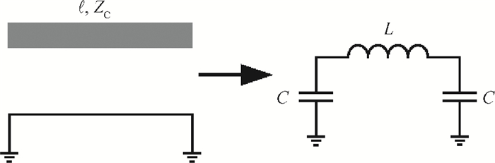
Fig. 1.
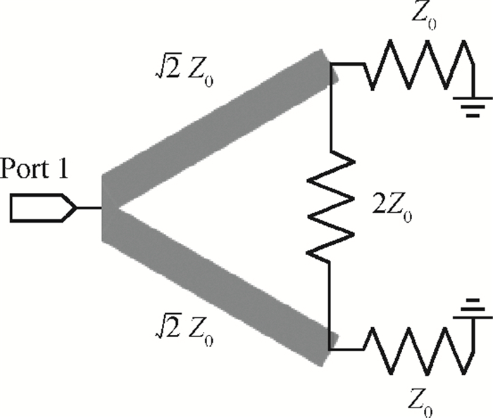
Wilkinson power divider.
SEMICONDUCTOR INTEGRATED CIRCUITS
Zebao Du, Hao Yang, Haiying Zhang and Min Zhu
Corresponding author: Du Zebao, Email:duzebao@ime.ac.cn
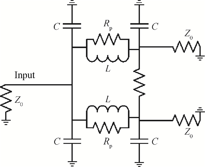
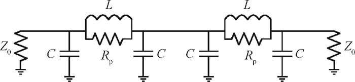
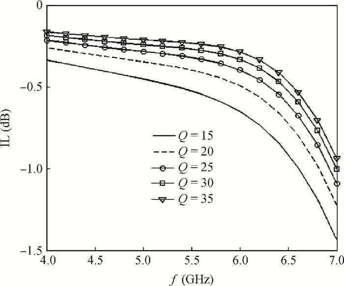
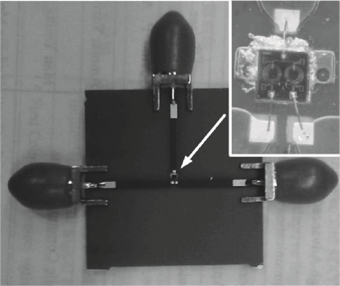
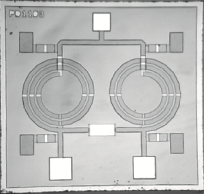
Abstract: A compact lumped integrated power divider with low insertion loss using 0.5 μm GaAs pHEMT technology is presented. The proposed power divider uses the π-type LC network for transmission line equivalence and a thin film resistor for isolation tuning simultaneously. The quality factor of the inductor is analyzed and synthesized for insertion-loss influence. The measured insertion loss is less than 0.5 dB when the operating frequency is within the range of 5.15-6.15 GHz. The return loss and isolation are better than 15 dB and 20 dB, respectively. The compact dimension of the power divider is as small as 0.9×0.85 mm2. The measured results agree well with the simulated ones.
Keywords: power divider, GaAs, IPD
| [1] |
Grebennikov A. RF and microwave transmitter design. New York: Wiley, 2011 http://ci.nii.ac.jp/ncid/BB06505372
|
| [2] |
Pozar D M. Microwave engineering. 3rd ed. New York: Wiley, 2005 https://www.researchgate.net/publication/308449120_Microwave_Engineering
|
| [3] |
Kawai T, Ohta I, Enokihara A. Design method of lumped-element dual-band Wilkinson power dividers based on frequency transformation. Asia-Pacific Microwave Conference Proceedings, 2010:710 http://ieeexplore.ieee.org/document/5728440/
|
| [4] |
Lu L H, Liao Y T, Wu C R. A miniaturized Wilkinson power divider with CMOS active inductors. IEEE Microw Wireless Compon Lett, 2005, 15(11):775 doi: 10.1109/LMWC.2005.859020
|
| [5] |
Kim H T, Liu K, Frye R C, et al. Design of compact power divider using integrated passive device (IPD) technology. Electronic Components and Technology Conference, 2009:1894 http://ieeexplore.ieee.org/xpls/icp.jsp?arnumber=5074278
|
| [6] |
Elsbury M M, Dresselhaus P D, Bergren N F, et al. Broadband lumped-element integrated n-way power dividers for voltage standards. IEEE Trans Microw Theory Tech, 2009, 57(8):2055 doi: 10.1109/TMTT.2009.2025464
|
| [7] |
Wang C, Qian C, Kyung G I, et al. High performance integrated passive technology by SI-GaAs-based fabrication for RF and microwave application. Asia-Pacific Microwave Conference Proceedings, 2008:1 http://ieeexplore.ieee.org/xpls/icp.jsp?arnumber=4958020
|
| [8] |
Wang C, Lee W S, Zhang F, et al. A novel method for the fabrication of integrated passive devices on SI-GaAs substrate. International Journal of Advanced Manufacturing Technology, 2011, 52:1011 doi: 10.1007/s00170-010-2807-z
|
| [9] |
Lin Y S, Lee J H. Miniature ultra-wideband power divider using bridged T-coils. IEEE Microw Compon Lett, 2012, 22(8):391 doi: 10.1109/LMWC.2012.2205231
|
| [10] |
Wu Rui, Liao Xiaoping, Zhang Zhiqiang. MMIC-based RF on-chip LC passive filters. Journal of Semiconductors, 2008, 29(12):2437 http://www.jos.ac.cn/bdtxbcn/ch/reader/view_abstract.aspx?file_no=08041402&flag=1
|
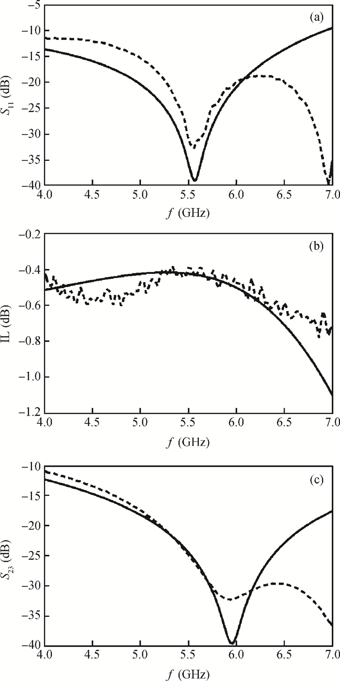
Table 1. Characteristics of different technologies.

|
Table 2. Comparison with previously reported high-performance power divider.

|
| [1] |
Grebennikov A. RF and microwave transmitter design. New York: Wiley, 2011 http://ci.nii.ac.jp/ncid/BB06505372
|
| [2] |
Pozar D M. Microwave engineering. 3rd ed. New York: Wiley, 2005 https://www.researchgate.net/publication/308449120_Microwave_Engineering
|
| [3] |
Kawai T, Ohta I, Enokihara A. Design method of lumped-element dual-band Wilkinson power dividers based on frequency transformation. Asia-Pacific Microwave Conference Proceedings, 2010:710 http://ieeexplore.ieee.org/document/5728440/
|
| [4] |
Lu L H, Liao Y T, Wu C R. A miniaturized Wilkinson power divider with CMOS active inductors. IEEE Microw Wireless Compon Lett, 2005, 15(11):775 doi: 10.1109/LMWC.2005.859020
|
| [5] |
Kim H T, Liu K, Frye R C, et al. Design of compact power divider using integrated passive device (IPD) technology. Electronic Components and Technology Conference, 2009:1894 http://ieeexplore.ieee.org/xpls/icp.jsp?arnumber=5074278
|
| [6] |
Elsbury M M, Dresselhaus P D, Bergren N F, et al. Broadband lumped-element integrated n-way power dividers for voltage standards. IEEE Trans Microw Theory Tech, 2009, 57(8):2055 doi: 10.1109/TMTT.2009.2025464
|
| [7] |
Wang C, Qian C, Kyung G I, et al. High performance integrated passive technology by SI-GaAs-based fabrication for RF and microwave application. Asia-Pacific Microwave Conference Proceedings, 2008:1 http://ieeexplore.ieee.org/xpls/icp.jsp?arnumber=4958020
|
| [8] |
Wang C, Lee W S, Zhang F, et al. A novel method for the fabrication of integrated passive devices on SI-GaAs substrate. International Journal of Advanced Manufacturing Technology, 2011, 52:1011 doi: 10.1007/s00170-010-2807-z
|
| [9] |
Lin Y S, Lee J H. Miniature ultra-wideband power divider using bridged T-coils. IEEE Microw Compon Lett, 2012, 22(8):391 doi: 10.1109/LMWC.2012.2205231
|
| [10] |
Wu Rui, Liao Xiaoping, Zhang Zhiqiang. MMIC-based RF on-chip LC passive filters. Journal of Semiconductors, 2008, 29(12):2437 http://www.jos.ac.cn/bdtxbcn/ch/reader/view_abstract.aspx?file_no=08041402&flag=1
|


Article views: 3611 Times PDF downloads: 23 Times Cited by: 0 Times
Received: 17 June 2013 Revised: 24 November 2013 Online: Published: 01 April 2014
| Citation: |
Zebao Du, Hao Yang, Haiying Zhang, Min Zhu. An integrated power divider implemented in GaAs technology[J]. Journal of Semiconductors, 2014, 35(4): 045003. doi: 10.1088/1674-4926/35/4/045003
****
Z B Du, H Yang, H Y Zhang, M Zhu. An integrated power divider implemented in GaAs technology[J]. J. Semicond., 2014, 35(4): 045003. doi: 10.1088/1674-4926/35/4/045003.

|
| [1] |
Grebennikov A. RF and microwave transmitter design. New York: Wiley, 2011 http://ci.nii.ac.jp/ncid/BB06505372
|
| [2] |
Pozar D M. Microwave engineering. 3rd ed. New York: Wiley, 2005 https://www.researchgate.net/publication/308449120_Microwave_Engineering
|
| [3] |
Kawai T, Ohta I, Enokihara A. Design method of lumped-element dual-band Wilkinson power dividers based on frequency transformation. Asia-Pacific Microwave Conference Proceedings, 2010:710 http://ieeexplore.ieee.org/document/5728440/
|
| [4] |
Lu L H, Liao Y T, Wu C R. A miniaturized Wilkinson power divider with CMOS active inductors. IEEE Microw Wireless Compon Lett, 2005, 15(11):775 doi: 10.1109/LMWC.2005.859020
|
| [5] |
Kim H T, Liu K, Frye R C, et al. Design of compact power divider using integrated passive device (IPD) technology. Electronic Components and Technology Conference, 2009:1894 http://ieeexplore.ieee.org/xpls/icp.jsp?arnumber=5074278
|
| [6] |
Elsbury M M, Dresselhaus P D, Bergren N F, et al. Broadband lumped-element integrated n-way power dividers for voltage standards. IEEE Trans Microw Theory Tech, 2009, 57(8):2055 doi: 10.1109/TMTT.2009.2025464
|
| [7] |
Wang C, Qian C, Kyung G I, et al. High performance integrated passive technology by SI-GaAs-based fabrication for RF and microwave application. Asia-Pacific Microwave Conference Proceedings, 2008:1 http://ieeexplore.ieee.org/xpls/icp.jsp?arnumber=4958020
|
| [8] |
Wang C, Lee W S, Zhang F, et al. A novel method for the fabrication of integrated passive devices on SI-GaAs substrate. International Journal of Advanced Manufacturing Technology, 2011, 52:1011 doi: 10.1007/s00170-010-2807-z
|
| [9] |
Lin Y S, Lee J H. Miniature ultra-wideband power divider using bridged T-coils. IEEE Microw Compon Lett, 2012, 22(8):391 doi: 10.1109/LMWC.2012.2205231
|
| [10] |
Wu Rui, Liao Xiaoping, Zhang Zhiqiang. MMIC-based RF on-chip LC passive filters. Journal of Semiconductors, 2008, 29(12):2437 http://www.jos.ac.cn/bdtxbcn/ch/reader/view_abstract.aspx?file_no=08041402&flag=1
|

 WeChat ID
Journal of Semiconductors © 2017 All Rights Reserved 京ICP备05085259号-2

 DownLoad: