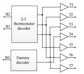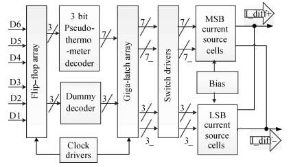
Fig. 1.
Block diagram of the designed 6-bit pseudo-thermometer segmented DAC.
SEMICONDUCTOR INTEGRATED CIRCUITS
Yijun Song and Wenyuan Li
Corresponding author: Li Wenyuan, Email:lwy555@seu.edu.cn
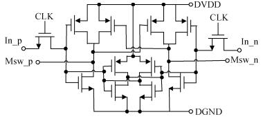
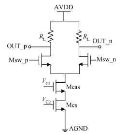
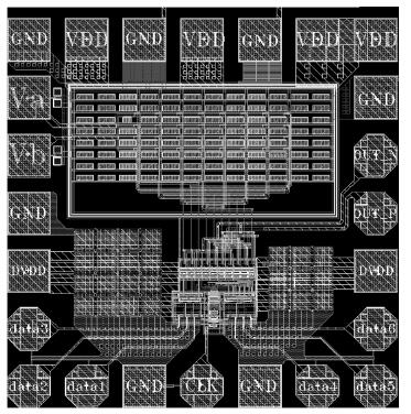
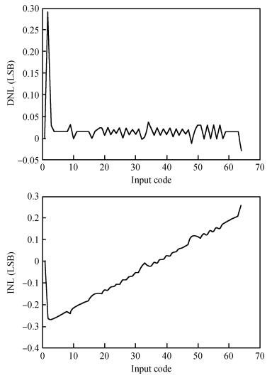
Abstract: A 6-bit 4 GS/s, high-speed and power-efficient DAC for ultra-high-speed transceivers in 60 GHz band millimeter wave technology is presented. A novel pseudo-thermometer architecture is proposed to realize a good compromise between the fast conversion speed and the chip area. Symmetrical and compact floor planning and layout techniques including tree-like routing, cross-quading and common-centroid method are adopted to guarantee the chip is fully functional up to near-Nyquist frequency in a standard 0.18 μm CMOS process. Post simulation results corroborate the feasibility of the designed DAC, which can perform good static and dynamic linearity without calibration. DNL errors and INL errors can be controlled within ±0.28 LSB and ±0.26 LSB, respectively. SFDR at 4 GHz clock frequency for a 1.9 GHz near-Nyquist sinusoidal output signal is 40.83 dB and the power dissipation is less than 37 mW.
Keywords: high speed DAC, CMOS, current-steering, near-Nyquist sampling
| [1] |
Wu X, Palmeras P, Steyaer M S J. A 130 nm CMOS 6-bit full Nyquist 3GS/s DAC. IEEE J Solid-State Circuits, 2008, 43:2396. doi: 10.1109/JSSC.2008.2004527
|
| [2] |
Bosch A V D, Borreamans M A F, Steyaert M S J, et al. A 10-bit 1-Gsample/s Nyquist current-steering CMOS D/A converter. IEEE J Solid-State Circuits, 2001, 36:315 doi: 10.1109/4.910469
|
| [3] |
Chen R L, Ting H W, Chang S J. Six-bit 2.7-GS/s 5.4-mW Nyquist complementary metal-oxide semiconductor digital-to-analogue converter for ultra-wideband transceivers. IEEE J IET Circuits Devices & Systems, 2011, 6:95 http://ieeexplore.ieee.org/xpl/articleDetails.jsp?tp=&arnumber=6177328&contentType=Journals+%26+Magazines&queryText%3D%28complementary+metal+oxide+semiconductor%3Cin%3Ede%29
|
| [4] |
Luschas S, Lee H S. Output impedance requirements for DACs. ISCAS, 2003, 1:I-861 http://ieeexplore.ieee.org/xpl/articleDetails.jsp?arnumber=1205700
|
| [5] |
Jung J, Baek K H, Lim S I, et al. Design of a 6 bit 1.25 GS/s DAC for WPAN. Proc Int Symp Circuits and Systems, 2008:2262 http://ieeexplore.ieee.org/lpdocs/epic03/wrapper.htm?arnumber=4541904
|
| [6] |
Narayanan A, Bengtsson M, Ragavan R, et al. A 0.35μm CMOS 6-bit current steering DAC. ECCTD, 2013:1 http://ieeexplore.ieee.org/document/6662280/
|
| [7] |
Seo D, McAllister G H. A low-spurious low-power 12-bit 160-MS/s DAC in 90-nm CMOS for baseband wireless transmitter. IEEE J Solid-State Circuits, 2007, 42:486 doi: 10.1109/JSSC.2006.891722
|
| [8] |
Van den Bosch A, Steyaert M, Sasen W. An accurate statistical yield for CMOS current-steering D/A converters. IEEE International Symposium on Circuits and Systems, 2000, Ⅳ:105 doi: 10.1023/A:1011261330190
|
| [9] |
Wu X, Steyaert M. A 90 nm CMOS 5-bit 2 GS/s DAC for UWB transceivers. IEEE ICUWB, 2010:20 http://ieeexplore.ieee.org/xpls/icp.jsp?arnumber=5614711
|
| [10] |
Deveugele J, Steyaert M S J. A 10-bit 250-MS/s binary-weighted current-steering DAC. IEEE J Solid-State Circuits, 2006, 41:320 doi: 10.1109/JSSC.2005.862342
|
| [11] |
Farzan K, Johns D A. A power-efficient architecture for high-speed D/A converters. Proc Int Symp Circuits and Systems, 2003:1-897 http://dblp.uni-trier.de/db/conf/iscas/iscas2003-1.html#FarzanJ03
|
| [12] |
Jung J J, Park B H, Choi S S, et al. A 6-bit 2.704 Gsps DAC for DS-CDMA UWB. Proc IEEE Asia Pacific Conf Circuits and Systems, 2006:347 http://ieeexplore.ieee.org/document/4145402/
|
| [13] |
Kim B C, Cho M H, Kim Y G, et al. A 1 V 6-bit 2.4 GSps Nyquist CMOS DAC for UWB systems. MWSYM, 2010:912 http://www.mendeley.com/research/1-v-6-bit-2-4-gs-s-nyquist-cmos-dac-uwb-systems-1/
|
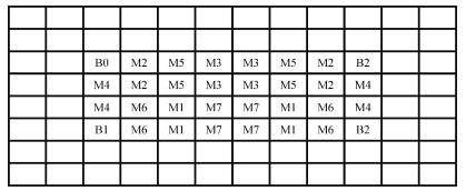
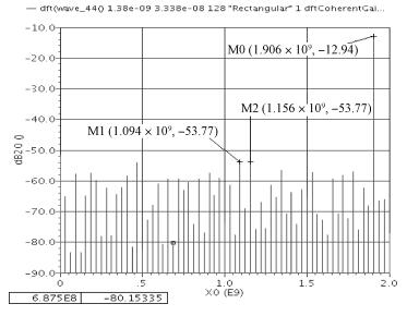
Table 1. Comparison of DAC systems with other published articles.

|
| [1] |
Wu X, Palmeras P, Steyaer M S J. A 130 nm CMOS 6-bit full Nyquist 3GS/s DAC. IEEE J Solid-State Circuits, 2008, 43:2396. doi: 10.1109/JSSC.2008.2004527
|
| [2] |
Bosch A V D, Borreamans M A F, Steyaert M S J, et al. A 10-bit 1-Gsample/s Nyquist current-steering CMOS D/A converter. IEEE J Solid-State Circuits, 2001, 36:315 doi: 10.1109/4.910469
|
| [3] |
Chen R L, Ting H W, Chang S J. Six-bit 2.7-GS/s 5.4-mW Nyquist complementary metal-oxide semiconductor digital-to-analogue converter for ultra-wideband transceivers. IEEE J IET Circuits Devices & Systems, 2011, 6:95 http://ieeexplore.ieee.org/xpl/articleDetails.jsp?tp=&arnumber=6177328&contentType=Journals+%26+Magazines&queryText%3D%28complementary+metal+oxide+semiconductor%3Cin%3Ede%29
|
| [4] |
Luschas S, Lee H S. Output impedance requirements for DACs. ISCAS, 2003, 1:I-861 http://ieeexplore.ieee.org/xpl/articleDetails.jsp?arnumber=1205700
|
| [5] |
Jung J, Baek K H, Lim S I, et al. Design of a 6 bit 1.25 GS/s DAC for WPAN. Proc Int Symp Circuits and Systems, 2008:2262 http://ieeexplore.ieee.org/lpdocs/epic03/wrapper.htm?arnumber=4541904
|
| [6] |
Narayanan A, Bengtsson M, Ragavan R, et al. A 0.35μm CMOS 6-bit current steering DAC. ECCTD, 2013:1 http://ieeexplore.ieee.org/document/6662280/
|
| [7] |
Seo D, McAllister G H. A low-spurious low-power 12-bit 160-MS/s DAC in 90-nm CMOS for baseband wireless transmitter. IEEE J Solid-State Circuits, 2007, 42:486 doi: 10.1109/JSSC.2006.891722
|
| [8] |
Van den Bosch A, Steyaert M, Sasen W. An accurate statistical yield for CMOS current-steering D/A converters. IEEE International Symposium on Circuits and Systems, 2000, Ⅳ:105 doi: 10.1023/A:1011261330190
|
| [9] |
Wu X, Steyaert M. A 90 nm CMOS 5-bit 2 GS/s DAC for UWB transceivers. IEEE ICUWB, 2010:20 http://ieeexplore.ieee.org/xpls/icp.jsp?arnumber=5614711
|
| [10] |
Deveugele J, Steyaert M S J. A 10-bit 250-MS/s binary-weighted current-steering DAC. IEEE J Solid-State Circuits, 2006, 41:320 doi: 10.1109/JSSC.2005.862342
|
| [11] |
Farzan K, Johns D A. A power-efficient architecture for high-speed D/A converters. Proc Int Symp Circuits and Systems, 2003:1-897 http://dblp.uni-trier.de/db/conf/iscas/iscas2003-1.html#FarzanJ03
|
| [12] |
Jung J J, Park B H, Choi S S, et al. A 6-bit 2.704 Gsps DAC for DS-CDMA UWB. Proc IEEE Asia Pacific Conf Circuits and Systems, 2006:347 http://ieeexplore.ieee.org/document/4145402/
|
| [13] |
Kim B C, Cho M H, Kim Y G, et al. A 1 V 6-bit 2.4 GSps Nyquist CMOS DAC for UWB systems. MWSYM, 2010:912 http://www.mendeley.com/research/1-v-6-bit-2-4-gs-s-nyquist-cmos-dac-uwb-systems-1/
|


Article views: 3044 Times PDF downloads: 33 Times Cited by: 0 Times
Received: 27 September 2013 Revised: 27 January 2014 Online: Published: 01 June 2014
| Citation: |
Yijun Song, Wenyuan Li. A 6-bit 4 GS/s pseudo-thermometer segmented CMOS DAC[J]. Journal of Semiconductors, 2014, 35(6): 065007. doi: 10.1088/1674-4926/35/6/065007
****
Y J Song, W Y Li. A 6-bit 4 GS/s pseudo-thermometer segmented CMOS DAC[J]. J. Semicond., 2014, 35(6): 065007. doi: 10.1088/1674-4926/35/6/065007.

|
| [1] |
Wu X, Palmeras P, Steyaer M S J. A 130 nm CMOS 6-bit full Nyquist 3GS/s DAC. IEEE J Solid-State Circuits, 2008, 43:2396. doi: 10.1109/JSSC.2008.2004527
|
| [2] |
Bosch A V D, Borreamans M A F, Steyaert M S J, et al. A 10-bit 1-Gsample/s Nyquist current-steering CMOS D/A converter. IEEE J Solid-State Circuits, 2001, 36:315 doi: 10.1109/4.910469
|
| [3] |
Chen R L, Ting H W, Chang S J. Six-bit 2.7-GS/s 5.4-mW Nyquist complementary metal-oxide semiconductor digital-to-analogue converter for ultra-wideband transceivers. IEEE J IET Circuits Devices & Systems, 2011, 6:95 http://ieeexplore.ieee.org/xpl/articleDetails.jsp?tp=&arnumber=6177328&contentType=Journals+%26+Magazines&queryText%3D%28complementary+metal+oxide+semiconductor%3Cin%3Ede%29
|
| [4] |
Luschas S, Lee H S. Output impedance requirements for DACs. ISCAS, 2003, 1:I-861 http://ieeexplore.ieee.org/xpl/articleDetails.jsp?arnumber=1205700
|
| [5] |
Jung J, Baek K H, Lim S I, et al. Design of a 6 bit 1.25 GS/s DAC for WPAN. Proc Int Symp Circuits and Systems, 2008:2262 http://ieeexplore.ieee.org/lpdocs/epic03/wrapper.htm?arnumber=4541904
|
| [6] |
Narayanan A, Bengtsson M, Ragavan R, et al. A 0.35μm CMOS 6-bit current steering DAC. ECCTD, 2013:1 http://ieeexplore.ieee.org/document/6662280/
|
| [7] |
Seo D, McAllister G H. A low-spurious low-power 12-bit 160-MS/s DAC in 90-nm CMOS for baseband wireless transmitter. IEEE J Solid-State Circuits, 2007, 42:486 doi: 10.1109/JSSC.2006.891722
|
| [8] |
Van den Bosch A, Steyaert M, Sasen W. An accurate statistical yield for CMOS current-steering D/A converters. IEEE International Symposium on Circuits and Systems, 2000, Ⅳ:105 doi: 10.1023/A:1011261330190
|
| [9] |
Wu X, Steyaert M. A 90 nm CMOS 5-bit 2 GS/s DAC for UWB transceivers. IEEE ICUWB, 2010:20 http://ieeexplore.ieee.org/xpls/icp.jsp?arnumber=5614711
|
| [10] |
Deveugele J, Steyaert M S J. A 10-bit 250-MS/s binary-weighted current-steering DAC. IEEE J Solid-State Circuits, 2006, 41:320 doi: 10.1109/JSSC.2005.862342
|
| [11] |
Farzan K, Johns D A. A power-efficient architecture for high-speed D/A converters. Proc Int Symp Circuits and Systems, 2003:1-897 http://dblp.uni-trier.de/db/conf/iscas/iscas2003-1.html#FarzanJ03
|
| [12] |
Jung J J, Park B H, Choi S S, et al. A 6-bit 2.704 Gsps DAC for DS-CDMA UWB. Proc IEEE Asia Pacific Conf Circuits and Systems, 2006:347 http://ieeexplore.ieee.org/document/4145402/
|
| [13] |
Kim B C, Cho M H, Kim Y G, et al. A 1 V 6-bit 2.4 GSps Nyquist CMOS DAC for UWB systems. MWSYM, 2010:912 http://www.mendeley.com/research/1-v-6-bit-2-4-gs-s-nyquist-cmos-dac-uwb-systems-1/
|

 WeChat ID
Journal of Semiconductors © 2017 All Rights Reserved 京ICP备05085259号-2

 DownLoad: