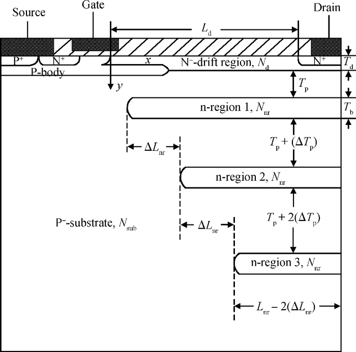
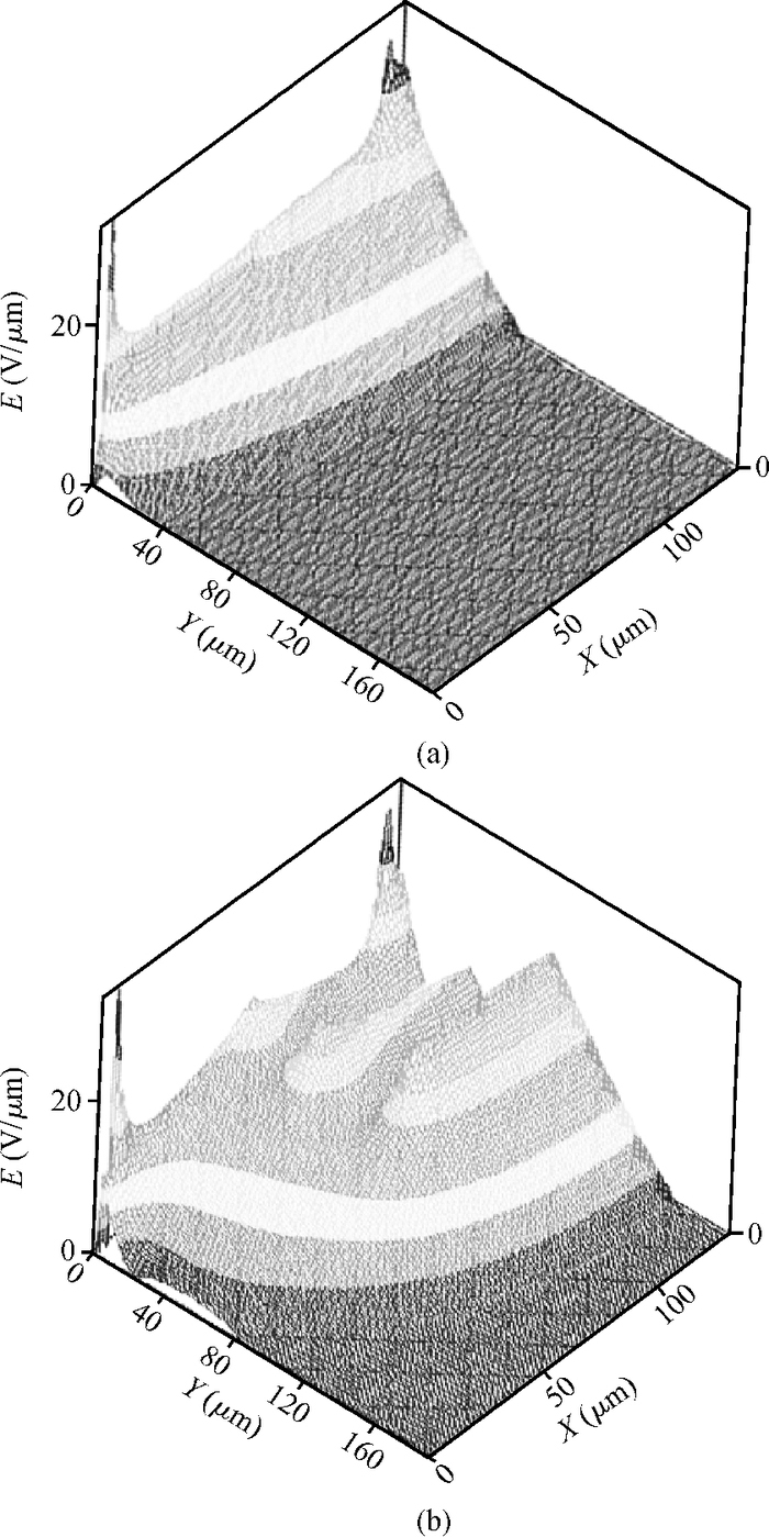
Fig. 1.
Cross-section of the MNR-LDMOST (n = 3).
SEMICONDUCTOR DEVICES
Jianbing Cheng1, 2, , Xiaojuan Xia1, Tong Jian1, Yufeng Guo1, Shujuan Yu1 and Hao Yang1
Corresponding author: Cheng Jianbing, Email:chengjianb@163.com
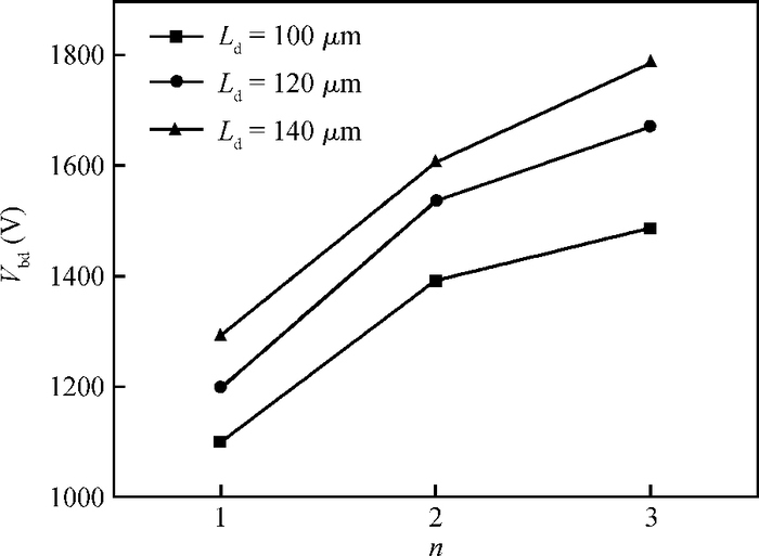
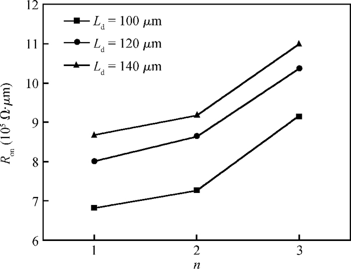
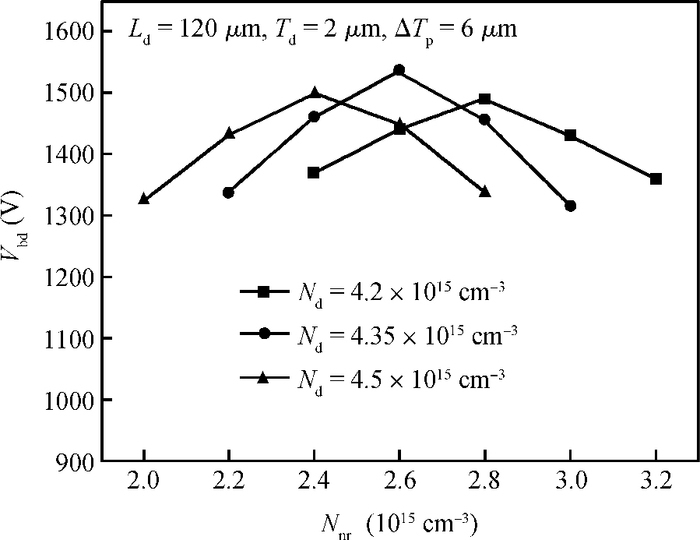
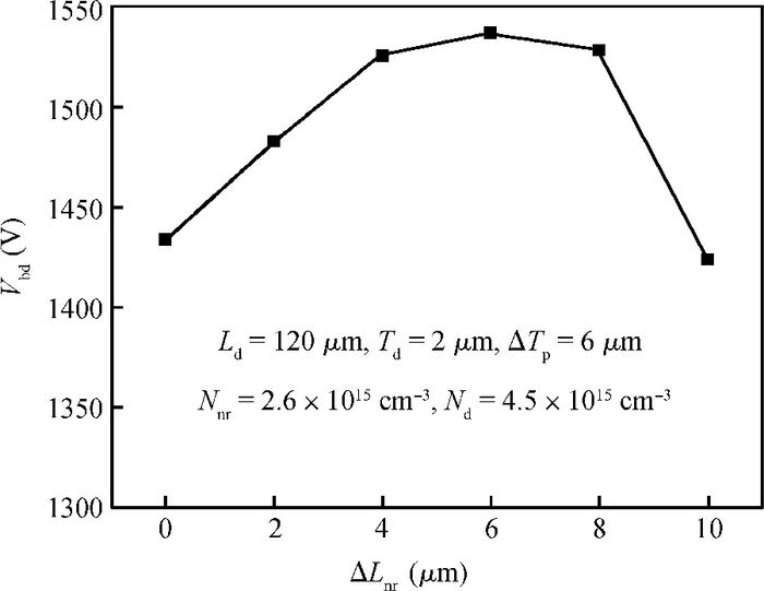
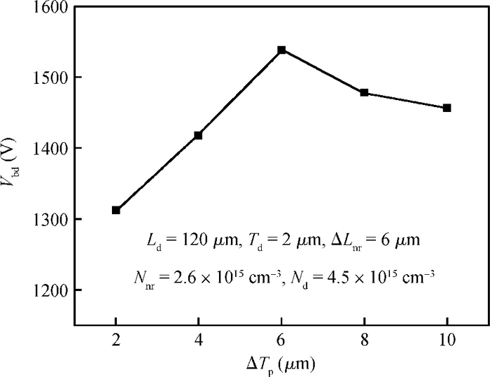
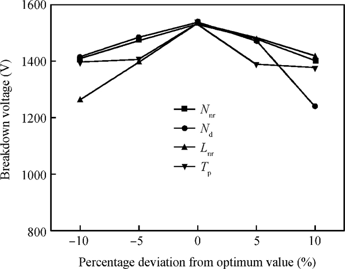
Abstract: A lateral double-diffused metal-oxide-semiconductor field effect transistor (LDMOST) with multiple n-regions in the p-substrate is investigated in detail. Because of the decrescent n-regions, the electric field distribution is higher and more uniform, and the breakdown voltage of the new structure is increased by 95%, in comparison with that of a conventional counterpart without substrate n-regions. Based on the trade-off between the breakdown voltage and the on-resistance, the optimal number of n-regions and the other key parameters are achieved. Furthermore, sensitivity research shows that the breakdown voltage is relatively sensitive to the drift region doping and the n-regions' lengths.
Keywords: LDMOST, multiple decrescent and reverse charge regions, electric field, breakdown voltage, on-resistance
| [1] |
Shi L X, Jia K, Sun W F. A novel compact high-voltage LDMOS transistor model for circuit simulation. IEEE Trans Electron Devices, 2013, 60(1): 346 doi: 10.1109/TED.2012.2227116
|
| [2] |
Takaya H, Miyagi K, Hamada K. Advanced floating island and thick bottom oxide trench gate MOSFET (FITMOS) with reduced RonA during AC operation by passive hole and improved BVdssRonA trade-off by elliptical floating island. 19th International Symposium on Power Semiconductor Devices and IC's (ISPSD), 2007: 197
|
| [3] |
Apples J, Vaes H. A high voltage thin layer devices (RESURF devices). IEDM Tech Dig, 1979: 238 http://ieeexplore.ieee.org/stamp/stamp.jsp?tp=&arnumber=1480454
|
| [4] |
Hardikar S, Tadikonda R, Green D W, et al. Realizing high-voltage junction isolated LDMOS transistors with variation in lateral doping. IEEE Trans Electron Devices, 2004, 51(12): 2223 doi: 10.1109/TED.2004.839104
|
| [5] |
He J, Huang R, Zhang X, et al. Analytical model of three-dimensional effect on voltage and edge peak filed distributions and optimal space for planar junction with a single field limiting ring. Solid-State Electron, 2001, 45(1): 79 doi: 10.1016/S0038-1101(00)00226-4
|
| [6] |
Cheng J B, Zhang B, Li Z J. A novel 1200-V LDMOSFET with floating buried layer in substrate. IEEE Electron Device Lett, 2008, 29(6): 645 doi: 10.1109/LED.2008.922731
|
| [7] |
Cheng J B, Zhang B, Duan B X, et al. A novel super-junction LDMOS with N-type step doping buffer layer. Chin Phys Lett, 2008, 25(1): 262 doi: 10.1088/0256-307X/25/1/071
|


Article views: 3227 Times PDF downloads: 12 Times Cited by: 0 Times
Received: 25 December 2013 Revised: 05 February 2014 Online: Published: 01 July 2014
| Citation: |
Jianbing Cheng, Xiaojuan Xia, Tong Jian, Yufeng Guo, Shujuan Yu, Hao Yang. Electric field optimized LDMOST using multiple decrescent and reverse charge regions[J]. Journal of Semiconductors, 2014, 35(7): 074007. doi: 10.1088/1674-4926/35/7/074007
****
J B Cheng, X J Xia, T Jian, Y F Guo, S J Yu, H Yang. Electric field optimized LDMOST using multiple decrescent and reverse charge regions[J]. J. Semicond., 2014, 35(7): 074007. doi: 10.1088/1674-4926/35/7/074007.

|
| [1] |
Shi L X, Jia K, Sun W F. A novel compact high-voltage LDMOS transistor model for circuit simulation. IEEE Trans Electron Devices, 2013, 60(1): 346 doi: 10.1109/TED.2012.2227116
|
| [2] |
Takaya H, Miyagi K, Hamada K. Advanced floating island and thick bottom oxide trench gate MOSFET (FITMOS) with reduced RonA during AC operation by passive hole and improved BVdssRonA trade-off by elliptical floating island. 19th International Symposium on Power Semiconductor Devices and IC's (ISPSD), 2007: 197
|
| [3] |
Apples J, Vaes H. A high voltage thin layer devices (RESURF devices). IEDM Tech Dig, 1979: 238 http://ieeexplore.ieee.org/stamp/stamp.jsp?tp=&arnumber=1480454
|
| [4] |
Hardikar S, Tadikonda R, Green D W, et al. Realizing high-voltage junction isolated LDMOS transistors with variation in lateral doping. IEEE Trans Electron Devices, 2004, 51(12): 2223 doi: 10.1109/TED.2004.839104
|
| [5] |
He J, Huang R, Zhang X, et al. Analytical model of three-dimensional effect on voltage and edge peak filed distributions and optimal space for planar junction with a single field limiting ring. Solid-State Electron, 2001, 45(1): 79 doi: 10.1016/S0038-1101(00)00226-4
|
| [6] |
Cheng J B, Zhang B, Li Z J. A novel 1200-V LDMOSFET with floating buried layer in substrate. IEEE Electron Device Lett, 2008, 29(6): 645 doi: 10.1109/LED.2008.922731
|
| [7] |
Cheng J B, Zhang B, Duan B X, et al. A novel super-junction LDMOS with N-type step doping buffer layer. Chin Phys Lett, 2008, 25(1): 262 doi: 10.1088/0256-307X/25/1/071
|

 WeChat ID
Journal of Semiconductors © 2017 All Rights Reserved 京ICP备05085259号-2

 DownLoad: