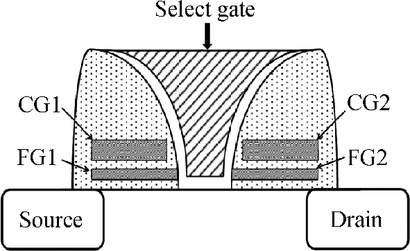
Fig. 1.
Schematic diagram of this flash cell.
SEMICONDUCTOR DEVICES
Liang Fang1, 2, 3, , Weiran Kong2, Jing Gu2, Bo Zhang2 and Shichang Zou1, 3
Corresponding author: Fang Liang, Email:fangliang@mail.sim.ac.cn
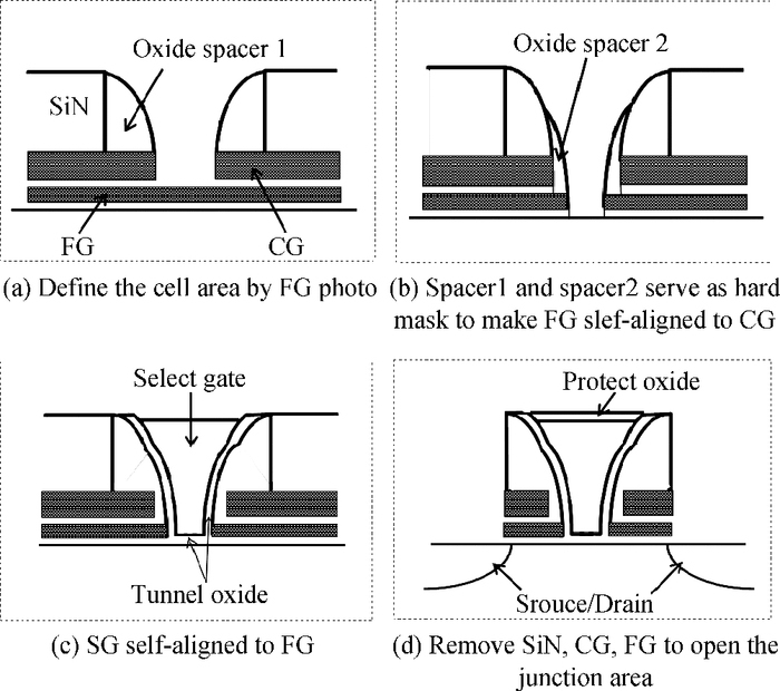
Abstract: A fully self-aligned symmetrical split-gate cell structure for 2-bit per cell flash memory with a very competitive bit size is presented. One common select gate is located between two floating gates and a pair of source/drain junctions are shared by the 2 bits. The fabrication method utilized here to create a self-aligned structure is to form a spacer against the prior layer without any additional mask. Although the cell consists of three channels in a series, the attributes from conventional split gate flash are still preserved with appropriate bias conditions. Program and erase operation is performed by using a source side injection (SSI) and a poly-to-poly tunneling mechanism respectively.
Keywords: split-gate flash, 2-bit per cell, self-aligned process
| [1] |
Houdt J V, Haspeslagh L, Wellekens D, et al. HIMOS-a high efficiency flash E2PROM cell for embedded memory applications. IEEE Trans Electron Devices, 1993, 40: 2255 doi: 10.1109/16.249473
|
| [2] |
Cho C Y S, Chen M J, Chen C F, et al. A novel self-aligned highly reliable sidewall split-gate flash memory. IEEE Trans Electron Devices, 2006, 53: 465 doi: 10.1109/TED.2005.863764
|
| [3] |
Shih H S, Fang S W, Kang A C, et al. High program efficiency of p-type floating gate in n-channel split-gate embedded flash memory. Appl Phys Lett, 2008, 93: 213503 doi: 10.1063/1.3023057
|
| [4] |
Chu W T, Lin H H, Hsieh C T, et al. Shrinkable triple self-aligned field-enhanced split-gate flash memory. IEEE Trans Electron Devices, 2004, 51: 1667 doi: 10.1109/TED.2004.835995
|
| [5] |
Wu M Y, Lin H H, Hu S F, et al. Highly scalable ballistic injection AND-type (BiAND) flash memory. IEEE Trans Electron Devices, 2006, 53: 109 doi: 10.1109/TED.2005.860636
|
| [6] |
Eitan B, Pavan P, Bloom I, et al. NROM: a novel localized trapping, 2-bit nonvolatile memory cell. IEEE Electron Device Lett, 2000, 22: 543 http://ieeexplore.ieee.org/xpl/articleDetails.jsp?arnumber=877205&contentType=Journals+%26+Magazines
|
| [7] |
Houdt J V, Wellekens D, Groeseneken G, et al. Investigation of the soft-write mechanism in source-side injection flash EEPROM devices. IEEE Trans Electron Devices, 1995, 16: 181 doi: 10.1109/55.382233
|
| [8] |
Breuil L, Haspeslagh L, Blomme, et al. A new scalable self-aligned dual-bit split-gate charge-trapping memory device. IEEE Trans Electron Devices, 2005, 52: 2250 doi: 10.1109/TED.2005.856803
|
| [9] |
Lue H T, Hsu T H, Wu M T, et al. Studies of the reverse read method and second-bit effect of 2-bit/cell nitride-trapping device by quasi-two-dimensional model. IEEE Trans Electron Devices, 2006, 53: 119 doi: 10.1109/TED.2005.860644
|
| [10] |
Yuri T, Xian L, Alexander K. Floating-gate corner-enhanced poly-to-poly tunneling in split-gate flash memory cells. IEEE Trans Electron Devices, 2012, 59: 5 doi: 10.1109/TED.2011.2171346
|

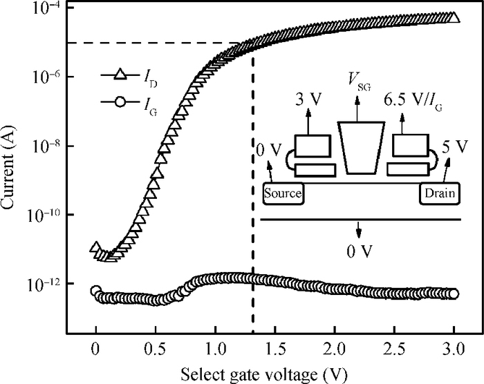
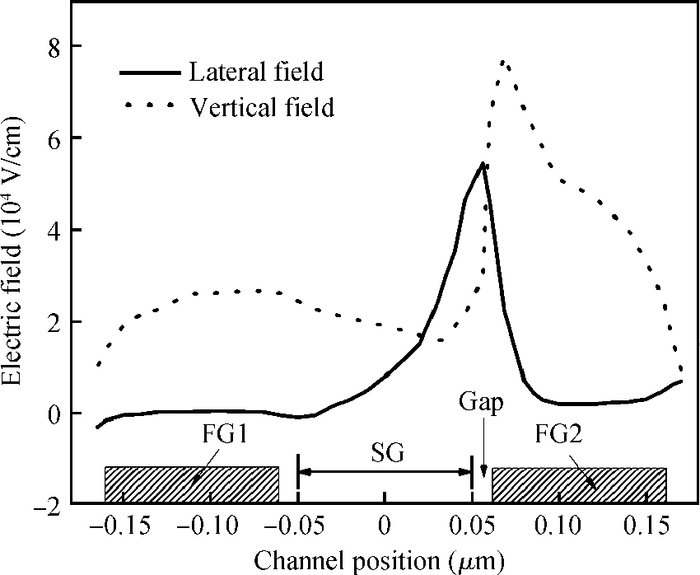
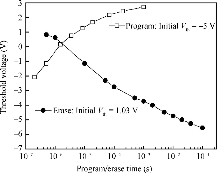
Table 1. Cell operation conditions (Unit: V).
 |
| [1] |
Houdt J V, Haspeslagh L, Wellekens D, et al. HIMOS-a high efficiency flash E2PROM cell for embedded memory applications. IEEE Trans Electron Devices, 1993, 40: 2255 doi: 10.1109/16.249473
|
| [2] |
Cho C Y S, Chen M J, Chen C F, et al. A novel self-aligned highly reliable sidewall split-gate flash memory. IEEE Trans Electron Devices, 2006, 53: 465 doi: 10.1109/TED.2005.863764
|
| [3] |
Shih H S, Fang S W, Kang A C, et al. High program efficiency of p-type floating gate in n-channel split-gate embedded flash memory. Appl Phys Lett, 2008, 93: 213503 doi: 10.1063/1.3023057
|
| [4] |
Chu W T, Lin H H, Hsieh C T, et al. Shrinkable triple self-aligned field-enhanced split-gate flash memory. IEEE Trans Electron Devices, 2004, 51: 1667 doi: 10.1109/TED.2004.835995
|
| [5] |
Wu M Y, Lin H H, Hu S F, et al. Highly scalable ballistic injection AND-type (BiAND) flash memory. IEEE Trans Electron Devices, 2006, 53: 109 doi: 10.1109/TED.2005.860636
|
| [6] |
Eitan B, Pavan P, Bloom I, et al. NROM: a novel localized trapping, 2-bit nonvolatile memory cell. IEEE Electron Device Lett, 2000, 22: 543 http://ieeexplore.ieee.org/xpl/articleDetails.jsp?arnumber=877205&contentType=Journals+%26+Magazines
|
| [7] |
Houdt J V, Wellekens D, Groeseneken G, et al. Investigation of the soft-write mechanism in source-side injection flash EEPROM devices. IEEE Trans Electron Devices, 1995, 16: 181 doi: 10.1109/55.382233
|
| [8] |
Breuil L, Haspeslagh L, Blomme, et al. A new scalable self-aligned dual-bit split-gate charge-trapping memory device. IEEE Trans Electron Devices, 2005, 52: 2250 doi: 10.1109/TED.2005.856803
|
| [9] |
Lue H T, Hsu T H, Wu M T, et al. Studies of the reverse read method and second-bit effect of 2-bit/cell nitride-trapping device by quasi-two-dimensional model. IEEE Trans Electron Devices, 2006, 53: 119 doi: 10.1109/TED.2005.860644
|
| [10] |
Yuri T, Xian L, Alexander K. Floating-gate corner-enhanced poly-to-poly tunneling in split-gate flash memory cells. IEEE Trans Electron Devices, 2012, 59: 5 doi: 10.1109/TED.2011.2171346
|


Article views: 4456 Times PDF downloads: 75 Times Cited by: 0 Times
Received: 18 December 2013 Revised: 26 January 2014 Online: Published: 01 July 2014
| Citation: |
Liang Fang, Weiran Kong, Jing Gu, Bo Zhang, Shichang Zou. A novel symmetrical split-gate structure for 2-bit per cell flash memory[J]. Journal of Semiconductors, 2014, 35(7): 074008. doi: 10.1088/1674-4926/35/7/074008
****
L Fang, W R Kong, J Gu, B Zhang, S C Zou. A novel symmetrical split-gate structure for 2-bit per cell flash memory[J]. J. Semicond., 2014, 35(7): 074008. doi: 10.1088/1674-4926/35/7/074008.

|
| [1] |
Houdt J V, Haspeslagh L, Wellekens D, et al. HIMOS-a high efficiency flash E2PROM cell for embedded memory applications. IEEE Trans Electron Devices, 1993, 40: 2255 doi: 10.1109/16.249473
|
| [2] |
Cho C Y S, Chen M J, Chen C F, et al. A novel self-aligned highly reliable sidewall split-gate flash memory. IEEE Trans Electron Devices, 2006, 53: 465 doi: 10.1109/TED.2005.863764
|
| [3] |
Shih H S, Fang S W, Kang A C, et al. High program efficiency of p-type floating gate in n-channel split-gate embedded flash memory. Appl Phys Lett, 2008, 93: 213503 doi: 10.1063/1.3023057
|
| [4] |
Chu W T, Lin H H, Hsieh C T, et al. Shrinkable triple self-aligned field-enhanced split-gate flash memory. IEEE Trans Electron Devices, 2004, 51: 1667 doi: 10.1109/TED.2004.835995
|
| [5] |
Wu M Y, Lin H H, Hu S F, et al. Highly scalable ballistic injection AND-type (BiAND) flash memory. IEEE Trans Electron Devices, 2006, 53: 109 doi: 10.1109/TED.2005.860636
|
| [6] |
Eitan B, Pavan P, Bloom I, et al. NROM: a novel localized trapping, 2-bit nonvolatile memory cell. IEEE Electron Device Lett, 2000, 22: 543 http://ieeexplore.ieee.org/xpl/articleDetails.jsp?arnumber=877205&contentType=Journals+%26+Magazines
|
| [7] |
Houdt J V, Wellekens D, Groeseneken G, et al. Investigation of the soft-write mechanism in source-side injection flash EEPROM devices. IEEE Trans Electron Devices, 1995, 16: 181 doi: 10.1109/55.382233
|
| [8] |
Breuil L, Haspeslagh L, Blomme, et al. A new scalable self-aligned dual-bit split-gate charge-trapping memory device. IEEE Trans Electron Devices, 2005, 52: 2250 doi: 10.1109/TED.2005.856803
|
| [9] |
Lue H T, Hsu T H, Wu M T, et al. Studies of the reverse read method and second-bit effect of 2-bit/cell nitride-trapping device by quasi-two-dimensional model. IEEE Trans Electron Devices, 2006, 53: 119 doi: 10.1109/TED.2005.860644
|
| [10] |
Yuri T, Xian L, Alexander K. Floating-gate corner-enhanced poly-to-poly tunneling in split-gate flash memory cells. IEEE Trans Electron Devices, 2012, 59: 5 doi: 10.1109/TED.2011.2171346
|

 WeChat ID
Journal of Semiconductors © 2017 All Rights Reserved 京ICP备05085259号-2

 DownLoad: