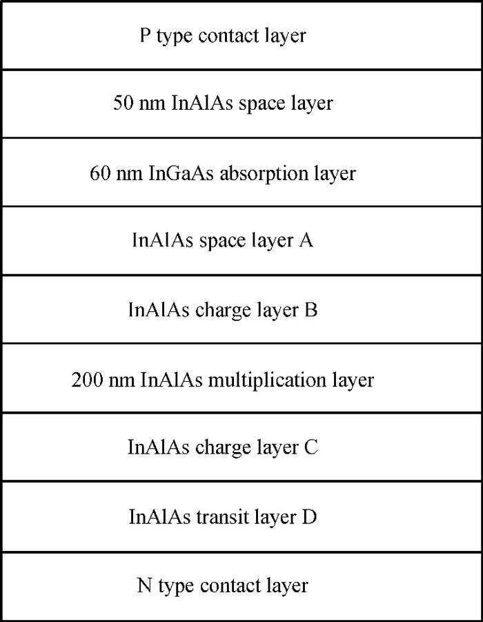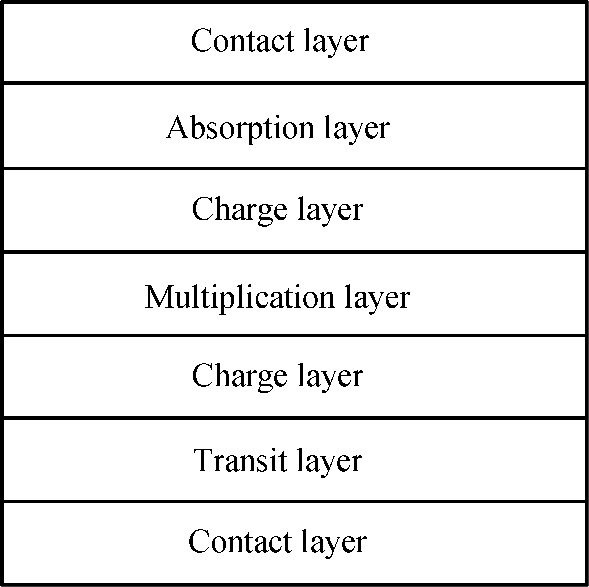
Fig. 1.
Schematic diagram of separate absorption charge multiplication charge and transit structure.
SEMICONDUCTOR DEVICES
Bin Li, Xiaohong Yang, Weihong Yin, Qianqian Lü, Rong Cui and Qin Han
Corresponding author: Han Qin, Email:hanqin@semi.ac.cn
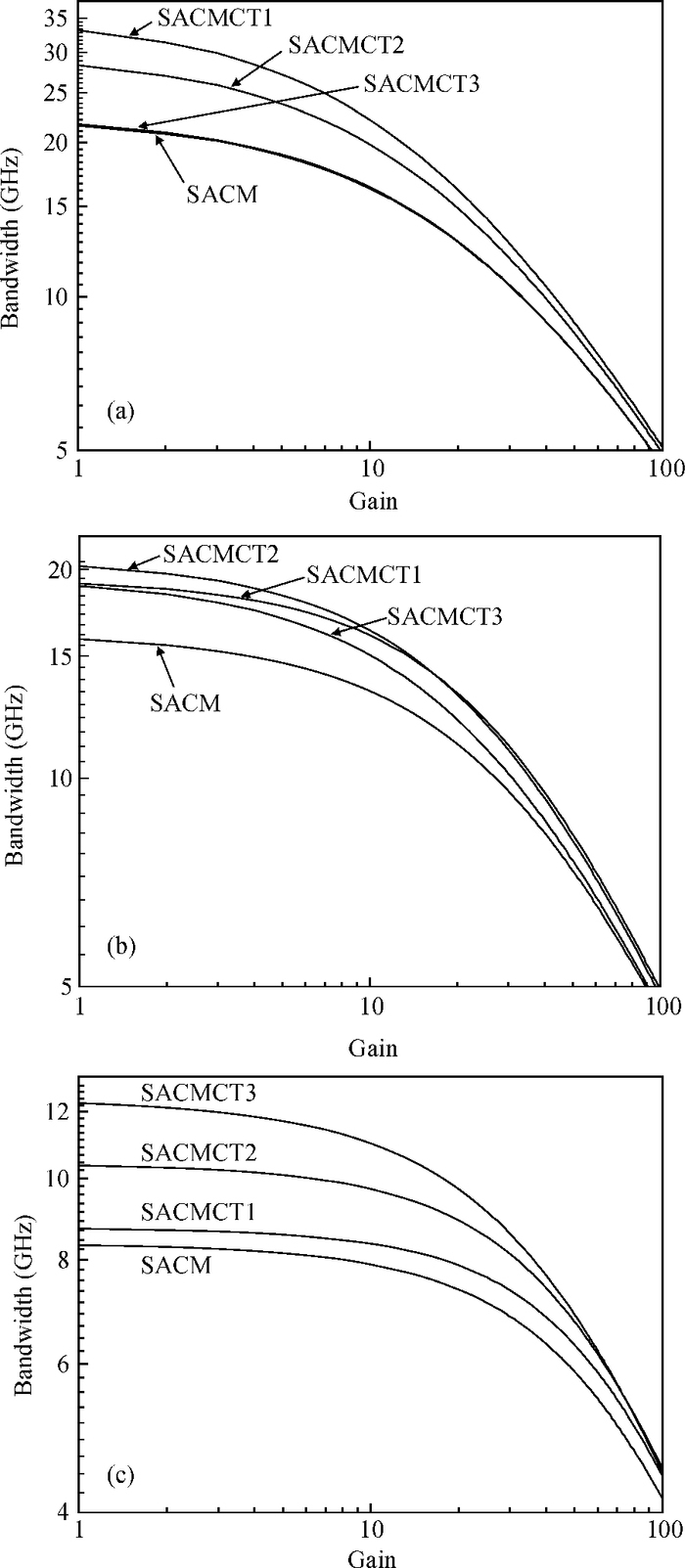
Abstract: High-speed avalanche photodiodes are widely used in optical communication systems. Nowadays, separate absorption charge and multiplication structure is widely adopted. In this article, a structure with higher speed than separate absorption charge and multiplication structure is reported. Besides the traditional absorption layer, charge layer and multiplication layer, this structure introduces an additional charge layer and transit layer and thus can be referred to as separate absorption, charge, multiplication, charge and transit structure. The introduction of the new charge layer and transit layer brings additional freedom in device structure design. The benefit of this structure is that the carrier transit time and device capacitance can be reduced independently, thus the 3 dB bandwidth could be improved by more than 50% in contrast to the separate absorption charge and multiplication structure with the same size.
Keywords: avalanche photodiodes, photodetector, high speed
| [1] |
Campbell J. Recent advances in telecommunications avalanche photodiodes. J Lightwave Technol, 2007, 25(1): 109 doi: 10.1109/JLT.2006.888481
|
| [2] |
Lenox C, Nie H, Yuan P, et al. Resonant-cavity InGaAs-InAlAs avalanche photodiodes with gain-bandwidth product of 290 GHz. IEEE Photonics Technol Lett, 1999, 11(9): 1162 doi: 10.1109/68.784238
|
| [3] |
Li N, Sidhu R, Li X, et al. InGaAs/InAlAs avalanche photodiode with undepleted absorber. Appl Phys Lett, 2003, 82(13): 2175 doi: 10.1063/1.1559437
|
| [4] |
Shi J W, Wu Z Y, Kuo F M. Planar InAlAs based separated absorption, transport, charge, and multiplication avalanche photodiode with large area and bandwidth-enhancement effect under high-sensitivity operation. 23RD Annual Meeting of the IEEE Photonics Society, 2010: 124 http://ieeexplore.ieee.org/document/5698789/
|
| [5] |
Kinsey G S, Campbell J C, Dentai A G. Waveguide avalanche photodiode operating at 1.55μm with a gain-bandwidth product of 320 GHz. IEEE Photonics Technol Lett, 2001, 13(8): 842 doi: 10.1109/68.935822
|
| [6] |
Demiguel S, Zheng X, Li N, et al. Evanescently-coupled avalanche photodiodes integrating a short multimode waveguide for high-responsivity and high-speed applications. Optical Fiber Communication Conference, 2004 https://www.osapublishing.org/viewmedia.cfm?URI=OFC-2004-TuM3&seq=0
|
| [7] |
Mai Y, Wang G. Equivalent circuit modeling of separate absorption grading charge multiplication avalanche photodiode. J Lightwave Technol, 2009, 27(9): 1197 doi: 10.1109/JLT.2008.929121
|
| [8] |
Lahrichi M, Glastre G, Derouin E, et al. 240-GHz gain-bandwidth product back-side illuminated AlInAs avalanche photodiodes. IEEE Photonics Technol Lett, 2010, 22(18): 1373 doi: 10.1109/LPT.2010.2057503
|
| [9] |
Yagyu E, Ishimura E, Nakaji M, et al. Design and characteristics of guardring-free planar AlInAs avalanche photodiodes. J Lightwave Technol, 2009, 27(8): 1011 doi: 10.1109/JLT.2008.2004954
|
| [10] |
Campbell J C, Demiguel S, Ma F, et al. Recent advances in avalanche photodiodes. IEEE J Sel Topics Quantum Electron, 2004, 10(4): 777 doi: 10.1109/JSTQE.2004.833971
|
| [11] |
Shimizu S, Shiba K, Nakata T, et al. 40 Gbit/s waveguide avalanche photodiode with p-type absorption layer and thin InAlAs multiplication layer. Electron Lett, 2007, 43(8): 476 doi: 10.1049/el:20070344
|
| [12] |
Duan N, Wang S, Ma F, et al. High-speed and low-noise SACM avalanche photodiodes with an impact-ionization-engineered multiplication region. IEEE Photonics Technol Lett, 2005, 17(8): 1719 doi: 10.1109/LPT.2005.851903
|


Article views: 4028 Times PDF downloads: 28 Times Cited by: 0 Times
Received: 27 November 2013 Revised: 08 January 2014 Online: Published: 01 July 2014
| Citation: |
Bin Li, Xiaohong Yang, Weihong Yin, Qianqian Lü, Rong Cui, Qin Han. A high-speed avalanche photodiode[J]. Journal of Semiconductors, 2014, 35(7): 074009. doi: 10.1088/1674-4926/35/7/074009
****
B Li, X H Yang, W H Yin, Q Lü, R Cui, Q Han. A high-speed avalanche photodiode[J]. J. Semicond., 2014, 35(7): 074009. doi: 10.1088/1674-4926/35/7/074009.

|
| [1] |
Campbell J. Recent advances in telecommunications avalanche photodiodes. J Lightwave Technol, 2007, 25(1): 109 doi: 10.1109/JLT.2006.888481
|
| [2] |
Lenox C, Nie H, Yuan P, et al. Resonant-cavity InGaAs-InAlAs avalanche photodiodes with gain-bandwidth product of 290 GHz. IEEE Photonics Technol Lett, 1999, 11(9): 1162 doi: 10.1109/68.784238
|
| [3] |
Li N, Sidhu R, Li X, et al. InGaAs/InAlAs avalanche photodiode with undepleted absorber. Appl Phys Lett, 2003, 82(13): 2175 doi: 10.1063/1.1559437
|
| [4] |
Shi J W, Wu Z Y, Kuo F M. Planar InAlAs based separated absorption, transport, charge, and multiplication avalanche photodiode with large area and bandwidth-enhancement effect under high-sensitivity operation. 23RD Annual Meeting of the IEEE Photonics Society, 2010: 124 http://ieeexplore.ieee.org/document/5698789/
|
| [5] |
Kinsey G S, Campbell J C, Dentai A G. Waveguide avalanche photodiode operating at 1.55μm with a gain-bandwidth product of 320 GHz. IEEE Photonics Technol Lett, 2001, 13(8): 842 doi: 10.1109/68.935822
|
| [6] |
Demiguel S, Zheng X, Li N, et al. Evanescently-coupled avalanche photodiodes integrating a short multimode waveguide for high-responsivity and high-speed applications. Optical Fiber Communication Conference, 2004 https://www.osapublishing.org/viewmedia.cfm?URI=OFC-2004-TuM3&seq=0
|
| [7] |
Mai Y, Wang G. Equivalent circuit modeling of separate absorption grading charge multiplication avalanche photodiode. J Lightwave Technol, 2009, 27(9): 1197 doi: 10.1109/JLT.2008.929121
|
| [8] |
Lahrichi M, Glastre G, Derouin E, et al. 240-GHz gain-bandwidth product back-side illuminated AlInAs avalanche photodiodes. IEEE Photonics Technol Lett, 2010, 22(18): 1373 doi: 10.1109/LPT.2010.2057503
|
| [9] |
Yagyu E, Ishimura E, Nakaji M, et al. Design and characteristics of guardring-free planar AlInAs avalanche photodiodes. J Lightwave Technol, 2009, 27(8): 1011 doi: 10.1109/JLT.2008.2004954
|
| [10] |
Campbell J C, Demiguel S, Ma F, et al. Recent advances in avalanche photodiodes. IEEE J Sel Topics Quantum Electron, 2004, 10(4): 777 doi: 10.1109/JSTQE.2004.833971
|
| [11] |
Shimizu S, Shiba K, Nakata T, et al. 40 Gbit/s waveguide avalanche photodiode with p-type absorption layer and thin InAlAs multiplication layer. Electron Lett, 2007, 43(8): 476 doi: 10.1049/el:20070344
|
| [12] |
Duan N, Wang S, Ma F, et al. High-speed and low-noise SACM avalanche photodiodes with an impact-ionization-engineered multiplication region. IEEE Photonics Technol Lett, 2005, 17(8): 1719 doi: 10.1109/LPT.2005.851903
|

 WeChat ID
Journal of Semiconductors © 2017 All Rights Reserved 京ICP备05085259号-2

 DownLoad: