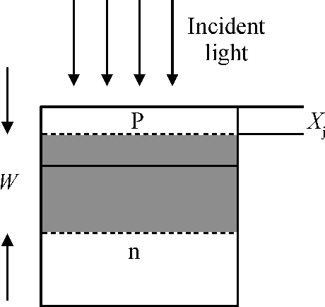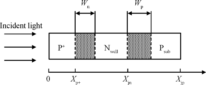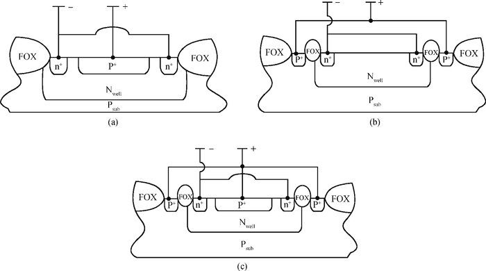
Fig. 1.
Schematic drawing of the three photodiode structures. (a) P+/Nwell. (b) Nwell/Psub. (c) P+/Nwell/Psub.
SEMICONDUCTOR DEVICES
Chaoqun Xu, Ying Sun, Yan Han and Dazhong Zhu
Corresponding author: Sun Ying, Email:suny@zju.edu.cn
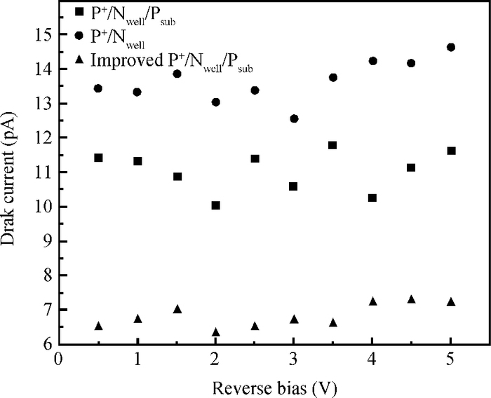
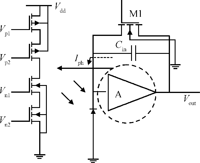
Abstract: A CMOS compatible P+/Nwell/Psub double junction photodiode pixel was proposed, which can efficiently detect fluorescence from CsI(Tl) scintillation in an X-ray sensor. Photoelectric and spectral responses of P+/Nwell, Nwell/Psub and P+/Nwell/Psub photodiodes were analyzed and modeled. Simulation results show P+/Nwell/Psub photodiode has larger photocurrent than P+/Nwell photodiode and Nwell/Psub photodiode, and its spectral response is more in accordance with CsI(Tl) fluorescence spectrum. Improved P+/Nwell/Psub photodiode detecting CsI(Tl) fluorescence was designed in CSMC 0.5 μm CMOS process, CTIA (capacitive transimpedance amplifier) architecture was used to readout photocurrent signal. CMOS X-ray sensor IC prototype contains 8×8 pixel array and pixel pitch is 100×100 μm2. Testing results show the dark current of the improved P+/Nwell/Psub photodiode (6.5 pA) is less than that of P+/Nwell and P+/Nwell/Psub photodiodes (13 pA and 11 pA respectively). The sensitivity of P+/Nwell/Psub photodiode is about 20 pA/lux under white LED. The spectrum response of P+/Nwell/Psub photodiode ranges from 400 nm to 800 nm with a peak at 532 nm, which is in accordance with the fluorescence spectrum of CsI(Tl) in an indirect X-ray sensor. Preliminary testing results show the sensitivity of X-ray sensor IC under Cu target X-ray is about 0.21 V·m2/W or 5097e-/pixel@8.05 keV considering the pixel size, integration time and average energy of X-ray photons.
Keywords: double junction photodiode, indirect X-ray sensor, CMOS X-ray sensor IC, fluorescence detection
| [1] |
Chavanelle J, Parmentier M. A CsI(Tl)-PIN photodiode gamma-ray probe. Nucl Instrum Methods Phys Res A, 2003, 504(1-3): 321 doi: 10.1016/S0168-9002(03)00761-7
|
| [2] |
Kah D H, Bae J B, Hyun H J, et al. Fabrication and performance test of a silicon photo-strip detector coupled with a crystal scintillator. Instrum Methods Phys Res A, 2011, 628(1-3): 256 http://linkinghub.elsevier.com/retrieve/pii/S0168900210015202
|
| [3] |
Silva J, Lanceros-Mendez S, Minas G, et al. CMOS X-ray image sensor array. Electronics, Circuits and Systems, 2007: 1067 doi: 10.1109/ICECS.2007.4511178
|
| [4] |
Kudin A M, Borodenko Y A, Grinyova B V, et al. CsI(Tl) + photodiode scintillation assemblies for γ -ray and proton detectors. Instruments and Experimental Techniques, 2010, 53(1): 39 doi: 10.1134/S0020441210010057
|
| [5] |
Miller S R, Gaysinskiy V, Shestakova I, et al. Recent advances in columnar CsI(Tl) scintillator screens. Proceedings of SPIE-Penetrating Radiation Systems and Applications Ⅶ, 2005, 5923-59230F: 1
|
| [6] |
Tabet M. Double sampling techniques for CMOS image sensors. PhD dissertation, University of Waterloo, Dept. Elect. Compt. Eng. , Waterloo, Ontario, Canada, 2002
|
| [7] |
Yamazaki T, Court L, Kameshima T. Sensor gain and noise requirements for fluoroscopic applications. Proceedings of SPIE-Physics of Medical Imaging, 2001, 2(25): 489 http://proceedings.spiedigitallibrary.org/pdfaccess.ashx?url=/data/conferences/spiep/35044/489_1.pdf
|
| [8] |
Valais I, Nikolopoulos D, Kalivas N, et al. A systematic study of the performance of the CsI:Tl single-crystal scintillator under X-ray excitation. Nucl Instrum Methods Phys Res A, 2007, 571(1/2): 343 http://linkinghub.elsevier.com/retrieve/pii/S0168900206018936
|
| [9] |
Murari K, Etienne-Cummings R, Thakor N, et al. Which photodiode to use: a comparison of CMOS-compatible structures. IEEE Sensors Journal, 2009, 9(7): 752 doi: 10.1109/JSEN.2009.2021805
|
| [10] |
Liu L N, Chen C, Liu C H. Numerical simulation of spectral response for 650 nm silicon photo detector. Semicond Photonics Technol, 2010, 2(9): 82
|
| [11] |
Dash W C, Newman R. Intrinsic optical absorption in single-crystal germanium and silicon at 77 K and 300 K. Phys Rev, 2007, 4(99): 145 http://adsabs.harvard.edu/abs/1955PhRv...99.1151D
|
| [12] |
Wu C Y, Shih Y C, Lan J F, et al. Design, optimization, and performance analysis of new photodiode structure s for CMOS active-pixel-sensor (APS) imager applications. IEEE Sensors Journal, 2004, 4(1): 135 doi: 10.1109/JSEN.2003.820361
|
| [13] |
Cheng H Y, King Y C. An ultra-low dark current CMOS image sensor cell using n/sup+/ring reset. IEEE Electron Device Lett, 2002, 23(9): 538 doi: 10.1109/LED.2002.802587
|
| [14] |
Liu C, Emadi A, Wu H W, et al. A CMOS 128-APS linear array integrated with a LVOF for high sensitivity and high-resolution micro-spectrophotometry. Proceedings of SPIE-The International Society for Optical Engineering, 2010, 7726: 772616 http://repository.tudelft.nl/islandora/object/uuid:ef511dec-c68d-4104-9861-b3ddc25b14d3/datastream/OBJ/download
|
| [15] |
Wang Xu, Yang Hongyan, Yuan Ying, et al. A low noise multi-channel readout IC for X-ray cargo inspection. Journal of Semiconductors, 2013, 34(4): 045011 doi: 10.1088/1674-4926/34/4/045011
|
| [16] |
Xu Jiangtao, Yao Suying, Li Binqiao, et al. Design, analysis, and optimization of a CMOS active pixel sensor. Chinese Journal of Semiconductor, 2006, 27(9): 1548 http://www.oalib.com/paper/1521963
|
| [17] |
Turchetta R, Berst J D, Casadei B, et al. A monolithic active pixel sensor for charged particle tracking and imaging using standard VLSI CMOS technology. Nuclear Instruments and Methods in Physics Research A, 2001, 458: 677 doi: 10.1016/S0168-9002(00)00893-7
|
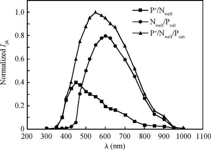
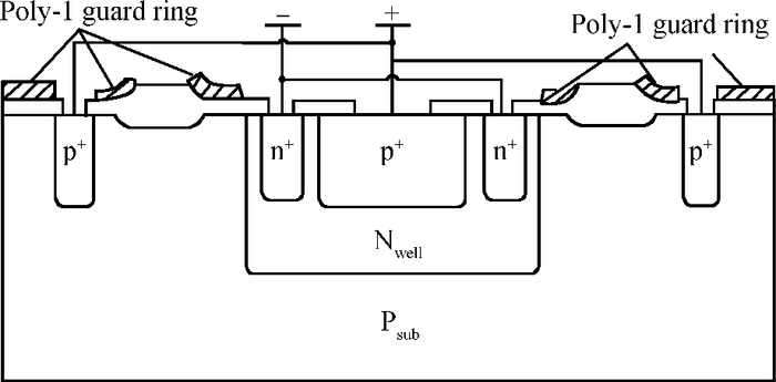
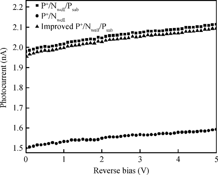
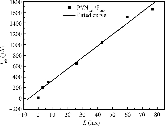
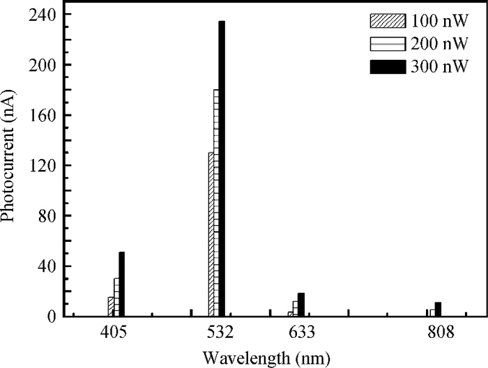
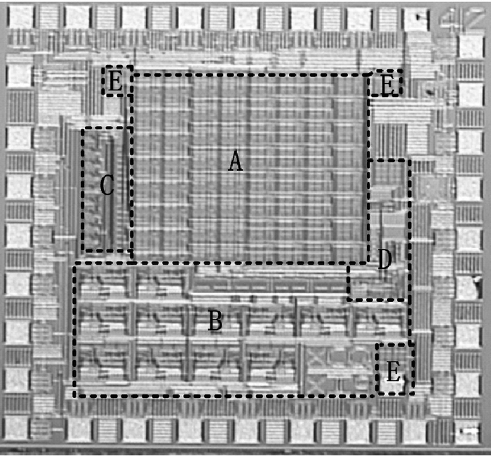
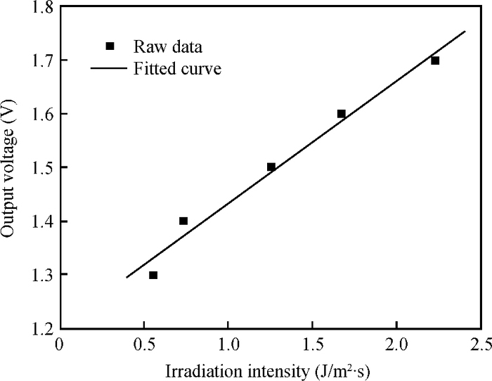
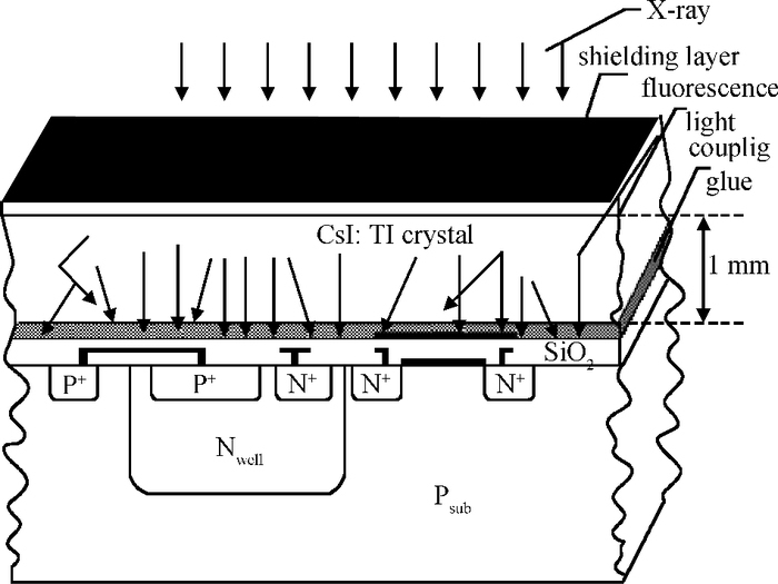
Table 1. Typical values of minority lifetime in silicon.
 |
Table 2. Comparison of the three photodiodes.
 |
Table 3. Testing results under X-ray excitation.
 |
Table 4. Main parameters of the sensor.
 |
| [1] |
Chavanelle J, Parmentier M. A CsI(Tl)-PIN photodiode gamma-ray probe. Nucl Instrum Methods Phys Res A, 2003, 504(1-3): 321 doi: 10.1016/S0168-9002(03)00761-7
|
| [2] |
Kah D H, Bae J B, Hyun H J, et al. Fabrication and performance test of a silicon photo-strip detector coupled with a crystal scintillator. Instrum Methods Phys Res A, 2011, 628(1-3): 256 http://linkinghub.elsevier.com/retrieve/pii/S0168900210015202
|
| [3] |
Silva J, Lanceros-Mendez S, Minas G, et al. CMOS X-ray image sensor array. Electronics, Circuits and Systems, 2007: 1067 doi: 10.1109/ICECS.2007.4511178
|
| [4] |
Kudin A M, Borodenko Y A, Grinyova B V, et al. CsI(Tl) + photodiode scintillation assemblies for γ -ray and proton detectors. Instruments and Experimental Techniques, 2010, 53(1): 39 doi: 10.1134/S0020441210010057
|
| [5] |
Miller S R, Gaysinskiy V, Shestakova I, et al. Recent advances in columnar CsI(Tl) scintillator screens. Proceedings of SPIE-Penetrating Radiation Systems and Applications Ⅶ, 2005, 5923-59230F: 1
|
| [6] |
Tabet M. Double sampling techniques for CMOS image sensors. PhD dissertation, University of Waterloo, Dept. Elect. Compt. Eng. , Waterloo, Ontario, Canada, 2002
|
| [7] |
Yamazaki T, Court L, Kameshima T. Sensor gain and noise requirements for fluoroscopic applications. Proceedings of SPIE-Physics of Medical Imaging, 2001, 2(25): 489 http://proceedings.spiedigitallibrary.org/pdfaccess.ashx?url=/data/conferences/spiep/35044/489_1.pdf
|
| [8] |
Valais I, Nikolopoulos D, Kalivas N, et al. A systematic study of the performance of the CsI:Tl single-crystal scintillator under X-ray excitation. Nucl Instrum Methods Phys Res A, 2007, 571(1/2): 343 http://linkinghub.elsevier.com/retrieve/pii/S0168900206018936
|
| [9] |
Murari K, Etienne-Cummings R, Thakor N, et al. Which photodiode to use: a comparison of CMOS-compatible structures. IEEE Sensors Journal, 2009, 9(7): 752 doi: 10.1109/JSEN.2009.2021805
|
| [10] |
Liu L N, Chen C, Liu C H. Numerical simulation of spectral response for 650 nm silicon photo detector. Semicond Photonics Technol, 2010, 2(9): 82
|
| [11] |
Dash W C, Newman R. Intrinsic optical absorption in single-crystal germanium and silicon at 77 K and 300 K. Phys Rev, 2007, 4(99): 145 http://adsabs.harvard.edu/abs/1955PhRv...99.1151D
|
| [12] |
Wu C Y, Shih Y C, Lan J F, et al. Design, optimization, and performance analysis of new photodiode structure s for CMOS active-pixel-sensor (APS) imager applications. IEEE Sensors Journal, 2004, 4(1): 135 doi: 10.1109/JSEN.2003.820361
|
| [13] |
Cheng H Y, King Y C. An ultra-low dark current CMOS image sensor cell using n/sup+/ring reset. IEEE Electron Device Lett, 2002, 23(9): 538 doi: 10.1109/LED.2002.802587
|
| [14] |
Liu C, Emadi A, Wu H W, et al. A CMOS 128-APS linear array integrated with a LVOF for high sensitivity and high-resolution micro-spectrophotometry. Proceedings of SPIE-The International Society for Optical Engineering, 2010, 7726: 772616 http://repository.tudelft.nl/islandora/object/uuid:ef511dec-c68d-4104-9861-b3ddc25b14d3/datastream/OBJ/download
|
| [15] |
Wang Xu, Yang Hongyan, Yuan Ying, et al. A low noise multi-channel readout IC for X-ray cargo inspection. Journal of Semiconductors, 2013, 34(4): 045011 doi: 10.1088/1674-4926/34/4/045011
|
| [16] |
Xu Jiangtao, Yao Suying, Li Binqiao, et al. Design, analysis, and optimization of a CMOS active pixel sensor. Chinese Journal of Semiconductor, 2006, 27(9): 1548 http://www.oalib.com/paper/1521963
|
| [17] |
Turchetta R, Berst J D, Casadei B, et al. A monolithic active pixel sensor for charged particle tracking and imaging using standard VLSI CMOS technology. Nuclear Instruments and Methods in Physics Research A, 2001, 458: 677 doi: 10.1016/S0168-9002(00)00893-7
|


Article views: 2944 Times PDF downloads: 27 Times Cited by: 0 Times
Received: 29 October 2013 Revised: 28 February 2014 Online: Published: 01 July 2014
| Citation: |
Chaoqun Xu, Ying Sun, Yan Han, Dazhong Zhu. Double junction photodiode for X-ray CMOS sensor IC[J]. Journal of Semiconductors, 2014, 35(7): 074011. doi: 10.1088/1674-4926/35/7/074011
****
C Q Xu, Y Sun, Y Han, D Z Zhu. Double junction photodiode for X-ray CMOS sensor IC[J]. J. Semicond., 2014, 35(7): 074011. doi: 10.1088/1674-4926/35/7/074011.

|
| [1] |
Chavanelle J, Parmentier M. A CsI(Tl)-PIN photodiode gamma-ray probe. Nucl Instrum Methods Phys Res A, 2003, 504(1-3): 321 doi: 10.1016/S0168-9002(03)00761-7
|
| [2] |
Kah D H, Bae J B, Hyun H J, et al. Fabrication and performance test of a silicon photo-strip detector coupled with a crystal scintillator. Instrum Methods Phys Res A, 2011, 628(1-3): 256 http://linkinghub.elsevier.com/retrieve/pii/S0168900210015202
|
| [3] |
Silva J, Lanceros-Mendez S, Minas G, et al. CMOS X-ray image sensor array. Electronics, Circuits and Systems, 2007: 1067 doi: 10.1109/ICECS.2007.4511178
|
| [4] |
Kudin A M, Borodenko Y A, Grinyova B V, et al. CsI(Tl) + photodiode scintillation assemblies for γ -ray and proton detectors. Instruments and Experimental Techniques, 2010, 53(1): 39 doi: 10.1134/S0020441210010057
|
| [5] |
Miller S R, Gaysinskiy V, Shestakova I, et al. Recent advances in columnar CsI(Tl) scintillator screens. Proceedings of SPIE-Penetrating Radiation Systems and Applications Ⅶ, 2005, 5923-59230F: 1
|
| [6] |
Tabet M. Double sampling techniques for CMOS image sensors. PhD dissertation, University of Waterloo, Dept. Elect. Compt. Eng. , Waterloo, Ontario, Canada, 2002
|
| [7] |
Yamazaki T, Court L, Kameshima T. Sensor gain and noise requirements for fluoroscopic applications. Proceedings of SPIE-Physics of Medical Imaging, 2001, 2(25): 489 http://proceedings.spiedigitallibrary.org/pdfaccess.ashx?url=/data/conferences/spiep/35044/489_1.pdf
|
| [8] |
Valais I, Nikolopoulos D, Kalivas N, et al. A systematic study of the performance of the CsI:Tl single-crystal scintillator under X-ray excitation. Nucl Instrum Methods Phys Res A, 2007, 571(1/2): 343 http://linkinghub.elsevier.com/retrieve/pii/S0168900206018936
|
| [9] |
Murari K, Etienne-Cummings R, Thakor N, et al. Which photodiode to use: a comparison of CMOS-compatible structures. IEEE Sensors Journal, 2009, 9(7): 752 doi: 10.1109/JSEN.2009.2021805
|
| [10] |
Liu L N, Chen C, Liu C H. Numerical simulation of spectral response for 650 nm silicon photo detector. Semicond Photonics Technol, 2010, 2(9): 82
|
| [11] |
Dash W C, Newman R. Intrinsic optical absorption in single-crystal germanium and silicon at 77 K and 300 K. Phys Rev, 2007, 4(99): 145 http://adsabs.harvard.edu/abs/1955PhRv...99.1151D
|
| [12] |
Wu C Y, Shih Y C, Lan J F, et al. Design, optimization, and performance analysis of new photodiode structure s for CMOS active-pixel-sensor (APS) imager applications. IEEE Sensors Journal, 2004, 4(1): 135 doi: 10.1109/JSEN.2003.820361
|
| [13] |
Cheng H Y, King Y C. An ultra-low dark current CMOS image sensor cell using n/sup+/ring reset. IEEE Electron Device Lett, 2002, 23(9): 538 doi: 10.1109/LED.2002.802587
|
| [14] |
Liu C, Emadi A, Wu H W, et al. A CMOS 128-APS linear array integrated with a LVOF for high sensitivity and high-resolution micro-spectrophotometry. Proceedings of SPIE-The International Society for Optical Engineering, 2010, 7726: 772616 http://repository.tudelft.nl/islandora/object/uuid:ef511dec-c68d-4104-9861-b3ddc25b14d3/datastream/OBJ/download
|
| [15] |
Wang Xu, Yang Hongyan, Yuan Ying, et al. A low noise multi-channel readout IC for X-ray cargo inspection. Journal of Semiconductors, 2013, 34(4): 045011 doi: 10.1088/1674-4926/34/4/045011
|
| [16] |
Xu Jiangtao, Yao Suying, Li Binqiao, et al. Design, analysis, and optimization of a CMOS active pixel sensor. Chinese Journal of Semiconductor, 2006, 27(9): 1548 http://www.oalib.com/paper/1521963
|
| [17] |
Turchetta R, Berst J D, Casadei B, et al. A monolithic active pixel sensor for charged particle tracking and imaging using standard VLSI CMOS technology. Nuclear Instruments and Methods in Physics Research A, 2001, 458: 677 doi: 10.1016/S0168-9002(00)00893-7
|

 WeChat ID
Journal of Semiconductors © 2017 All Rights Reserved 京ICP备05085259号-2

 DownLoad: