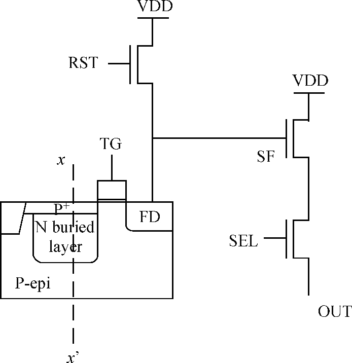
Fig. 1.
Basic 4-transistors CMOS image pixel configuration.
SEMICONDUCTOR DEVICES
Chen Cao, Bing Zhang, Longsheng Wu, Xin Li and Junfeng Wang
Corresponding author: Cao Chen, Email:intercaochen@163.com
Abstract: A novel analytical model of pinch-off voltage for CMOS image pixels with a pinned photodiode structure is proposed. The derived model takes account of the gradient doping distributions in the N buried layer due to the impurity compensation formed by manufacturing processes; the impurity distribution characteristics of two boundary PN junctions located in the region for particular spectrum response of a pinned photodiode are quantitative analyzed. By solving Poisson's equation in vertical barrier regions, the relationships between the pinch-off voltage and the corresponding process parameters such as peak doping concentration, N type width and doping concentration gradient of the N buried layer are established. Test results have shown that the derived model features the variations of the pinch-off voltage versus the process implant conditions more accurately than the traditional model. The research conclusions in this paper provide theoretical evidence for evaluating the pinch-off voltage design.
Keywords: pinned photodiode, pixel design, pinch-off voltage, analytical model
| [1] |
Fossum E R. CMOS image sensors: electronic camera-on-a-chip. IEEE Trans Electron Devices, 1997, 44: 1689 doi: 10.1109/16.628824
|
| [2] |
Lule T, Benthien S, Keller H, et al. Sensitivity of CMOS based imagers and scaling perspectives. IEEE Trans Electron Devices, 2000, 47: 2110 doi: 10.1109/16.877173
|
| [3] |
Inoue I, Tanaka N, Yamashita H, et al. Low leakage current and Low operating voltage buried photodiode for a CMOS imager. IEEE Trans Electron Devices, 2003, 50: 43 doi: 10.1109/TED.2002.807525
|
| [4] |
Li Binqiao, Yu Junting, Xu Jiangtao, et al. An approach to obtain the pinch-off voltage of 4-T pixel in CMOS image sensor. Journal of Semiconductors, 2010, 31(7): 074010 doi: 10.1088/1674-4926/31/7/074010
|
| [5] |
Bigas M, Cabruja E, Forest J, et al. Review of CMOS image sensors. Microelectron J, 2006, 37(5): 433 doi: 10.1016/j.mejo.2005.07.002
|
| [6] |
Krymski A I, Bock N E, Tu N, et al. Estimates for Scaling of Pinned Photodiodes. IEEE Workshop on CCD and Advanced Image Sensors, 2005: 60 http://m.alexima.com/pub/Scaling_Pinned.pdf
|
| [7] |
Park S, Uh H. The effect of size on photodiode pinch-off voltage for small pixel CMOS image sensors. Microelectron J, 2009, 40: 137 doi: 10.1016/j.mejo.2008.06.071
|
| [8] |
Zou Jijun, Chang Benkang, Yang Zhi. Theoretical calculation of quantum yield for exponential-doping GaAs photocathodes. Acta Phys Sin, 2007, 56: 2992(in Chinese) http://wulixb.iphy.ac.cn/EN/article/downloadArticleFile.do?attachType=PDF&id=12953
|
| [9] |
Adam G. Investigation of 4T CMOS image sensor design and the effects of radiation damage. PhM Dissertation, University of Surrey, UK, 2010: 5
|
| [10] |
Liu Enke, Zhu Bingsheng, Luo Jinsheng. Semiconductor physics. Beijing: Publishing House of Electronics Industry, 2008(in Chinese)
|
| [11] |
Lee P P, Guidash R M, Stevens E G, et al. Active pixel sensor integrated with a pinned photodiode. USA Patent, No. 5625210, 1997
|
| [12] |
Liang Bin, Chen Shuming, Liu Biwei. Using 3D TCAD simulation to study charge collection of a p-n junction in a 0.18μm bulk process. Journal of Semiconductors, 2008, 29(9): 1692 http://www.jos.ac.cn/bdtxben/ch/reader/view_abstract.aspx?file_no=08011003&flag=1
|
| [13] |
Simon M, Kwok K. Physics of semiconductor devices. Xi'an: Xi'an Jiaotong University Press, 2008(in Chinese)
|
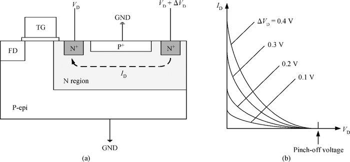
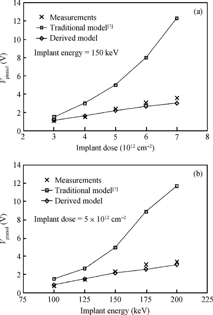
Table 1. Different implant doses with energy of 150 keV.
 |
Table 2. Different implant energies with dose of 5 × 1012 cm-2.
 |
| [1] |
Fossum E R. CMOS image sensors: electronic camera-on-a-chip. IEEE Trans Electron Devices, 1997, 44: 1689 doi: 10.1109/16.628824
|
| [2] |
Lule T, Benthien S, Keller H, et al. Sensitivity of CMOS based imagers and scaling perspectives. IEEE Trans Electron Devices, 2000, 47: 2110 doi: 10.1109/16.877173
|
| [3] |
Inoue I, Tanaka N, Yamashita H, et al. Low leakage current and Low operating voltage buried photodiode for a CMOS imager. IEEE Trans Electron Devices, 2003, 50: 43 doi: 10.1109/TED.2002.807525
|
| [4] |
Li Binqiao, Yu Junting, Xu Jiangtao, et al. An approach to obtain the pinch-off voltage of 4-T pixel in CMOS image sensor. Journal of Semiconductors, 2010, 31(7): 074010 doi: 10.1088/1674-4926/31/7/074010
|
| [5] |
Bigas M, Cabruja E, Forest J, et al. Review of CMOS image sensors. Microelectron J, 2006, 37(5): 433 doi: 10.1016/j.mejo.2005.07.002
|
| [6] |
Krymski A I, Bock N E, Tu N, et al. Estimates for Scaling of Pinned Photodiodes. IEEE Workshop on CCD and Advanced Image Sensors, 2005: 60 http://m.alexima.com/pub/Scaling_Pinned.pdf
|
| [7] |
Park S, Uh H. The effect of size on photodiode pinch-off voltage for small pixel CMOS image sensors. Microelectron J, 2009, 40: 137 doi: 10.1016/j.mejo.2008.06.071
|
| [8] |
Zou Jijun, Chang Benkang, Yang Zhi. Theoretical calculation of quantum yield for exponential-doping GaAs photocathodes. Acta Phys Sin, 2007, 56: 2992(in Chinese) http://wulixb.iphy.ac.cn/EN/article/downloadArticleFile.do?attachType=PDF&id=12953
|
| [9] |
Adam G. Investigation of 4T CMOS image sensor design and the effects of radiation damage. PhM Dissertation, University of Surrey, UK, 2010: 5
|
| [10] |
Liu Enke, Zhu Bingsheng, Luo Jinsheng. Semiconductor physics. Beijing: Publishing House of Electronics Industry, 2008(in Chinese)
|
| [11] |
Lee P P, Guidash R M, Stevens E G, et al. Active pixel sensor integrated with a pinned photodiode. USA Patent, No. 5625210, 1997
|
| [12] |
Liang Bin, Chen Shuming, Liu Biwei. Using 3D TCAD simulation to study charge collection of a p-n junction in a 0.18μm bulk process. Journal of Semiconductors, 2008, 29(9): 1692 http://www.jos.ac.cn/bdtxben/ch/reader/view_abstract.aspx?file_no=08011003&flag=1
|
| [13] |
Simon M, Kwok K. Physics of semiconductor devices. Xi'an: Xi'an Jiaotong University Press, 2008(in Chinese)
|


Article views: 3713 Times PDF downloads: 71 Times Cited by: 0 Times
Received: 29 November 2013 Revised: 20 January 2014 Online: Published: 01 July 2014
| Citation: |
Chen Cao, Bing Zhang, Longsheng Wu, Xin Li, Junfeng Wang. Pinch-off voltage modeling for CMOS image pixels with a pinned photodiode structure[J]. Journal of Semiconductors, 2014, 35(7): 074012. doi: 10.1088/1674-4926/35/7/074012
****
C Cao, B Zhang, L S Wu, X Li, J F Wang. Pinch-off voltage modeling for CMOS image pixels with a pinned photodiode structure[J]. J. Semicond., 2014, 35(7): 074012. doi: 10.1088/1674-4926/35/7/074012.

|
| [1] |
Fossum E R. CMOS image sensors: electronic camera-on-a-chip. IEEE Trans Electron Devices, 1997, 44: 1689 doi: 10.1109/16.628824
|
| [2] |
Lule T, Benthien S, Keller H, et al. Sensitivity of CMOS based imagers and scaling perspectives. IEEE Trans Electron Devices, 2000, 47: 2110 doi: 10.1109/16.877173
|
| [3] |
Inoue I, Tanaka N, Yamashita H, et al. Low leakage current and Low operating voltage buried photodiode for a CMOS imager. IEEE Trans Electron Devices, 2003, 50: 43 doi: 10.1109/TED.2002.807525
|
| [4] |
Li Binqiao, Yu Junting, Xu Jiangtao, et al. An approach to obtain the pinch-off voltage of 4-T pixel in CMOS image sensor. Journal of Semiconductors, 2010, 31(7): 074010 doi: 10.1088/1674-4926/31/7/074010
|
| [5] |
Bigas M, Cabruja E, Forest J, et al. Review of CMOS image sensors. Microelectron J, 2006, 37(5): 433 doi: 10.1016/j.mejo.2005.07.002
|
| [6] |
Krymski A I, Bock N E, Tu N, et al. Estimates for Scaling of Pinned Photodiodes. IEEE Workshop on CCD and Advanced Image Sensors, 2005: 60 http://m.alexima.com/pub/Scaling_Pinned.pdf
|
| [7] |
Park S, Uh H. The effect of size on photodiode pinch-off voltage for small pixel CMOS image sensors. Microelectron J, 2009, 40: 137 doi: 10.1016/j.mejo.2008.06.071
|
| [8] |
Zou Jijun, Chang Benkang, Yang Zhi. Theoretical calculation of quantum yield for exponential-doping GaAs photocathodes. Acta Phys Sin, 2007, 56: 2992(in Chinese) http://wulixb.iphy.ac.cn/EN/article/downloadArticleFile.do?attachType=PDF&id=12953
|
| [9] |
Adam G. Investigation of 4T CMOS image sensor design and the effects of radiation damage. PhM Dissertation, University of Surrey, UK, 2010: 5
|
| [10] |
Liu Enke, Zhu Bingsheng, Luo Jinsheng. Semiconductor physics. Beijing: Publishing House of Electronics Industry, 2008(in Chinese)
|
| [11] |
Lee P P, Guidash R M, Stevens E G, et al. Active pixel sensor integrated with a pinned photodiode. USA Patent, No. 5625210, 1997
|
| [12] |
Liang Bin, Chen Shuming, Liu Biwei. Using 3D TCAD simulation to study charge collection of a p-n junction in a 0.18μm bulk process. Journal of Semiconductors, 2008, 29(9): 1692 http://www.jos.ac.cn/bdtxben/ch/reader/view_abstract.aspx?file_no=08011003&flag=1
|
| [13] |
Simon M, Kwok K. Physics of semiconductor devices. Xi'an: Xi'an Jiaotong University Press, 2008(in Chinese)
|

 WeChat ID
Journal of Semiconductors © 2017 All Rights Reserved 京ICP备05085259号-2

 DownLoad: