


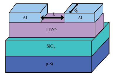
Fig. 1.
Schematic cross-sectional diagram of the a-ITZO TFT bottom-gate structure.
SEMICONDUCTOR DEVICES
Yongye Liang1, 2, Kyungsoo Jang2, S. Velumani3, Cam Phu Thi Nguyen2 and Junsin Yi2
Corresponding author: Junsin Yi, E-mail: yi@yurim.skku.ac.kr
Abstract: We reported the influence of interface trap density (Nt) on the electrical properties of amorphous InSnZnO based thin-film transistors, which were fabricated at different direct-current (DC) magnetron sputtering powers. The device with the smallest Nt of 5.68 × 1011 cm-2 and low resistivity of 1.21 × 10⁻³ Ω · cm exhibited a turn-on voltage (VON) of -3.60 V, a sub-threshold swing (S.S) of 0.16 V/dec and an on-off ratio (ION/IOFF) of ~ 8 × 10⁸. With increasing Nt, the VON, S.S and ION/IOFF were suppressed to —9.40 V, 0.24 V/dec and 2.59 × 10⁸, respectively. The VTH shift under negative gate bias stress has also been estimated to investigate the electrical stability of the devices. The result showed that the reduction in Nt contributes to an improvement in the electrical properties and stability.
Keywords: a-ITZO TFTs, low resistivity, interface trap density, electrical properties, electrical stability
| [1] | |
| [2] | |
| [3] | |
| [4] | |
| [5] | |
| [6] | |
| [7] | |
| [8] | |
| [9] | |
| [10] | |
| [11] | |
| [12] | |
| [13] | |
| [14] | |
| [15] | |
| [16] | |
| [17] | |
| [18] | |
| [19] | |
| [20] | |
| [21] | |
| [22] | |
| [23] | |
| [24] | |
| [25] | |
| [26] | |
| [27] | |
| [28] | |
| [29] |
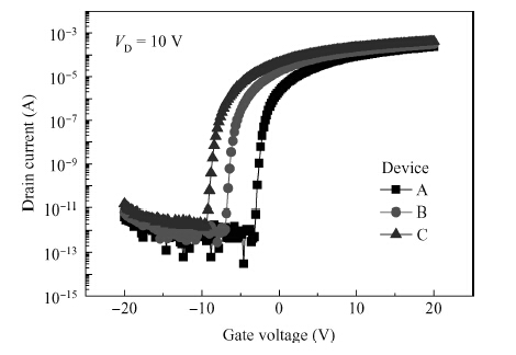
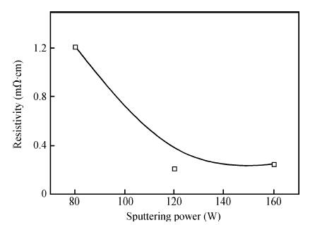
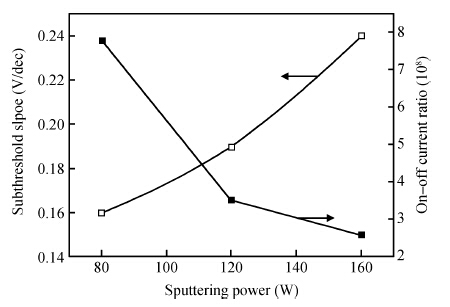
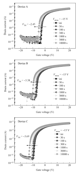
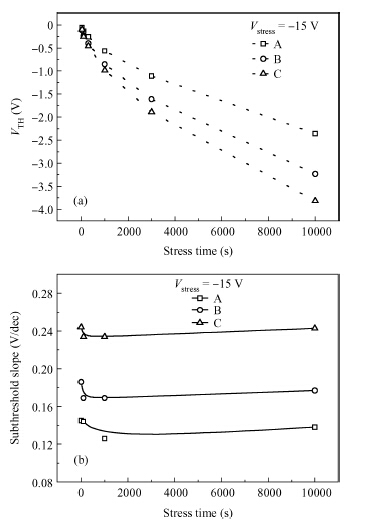
Table 1. Comparison of the extracted electrical properties including SS, $V_{\rm ON}$, $V_{\rm TH}$, $I_{\rm ON}$/$I_{\rm OFF}$, $N_{\rm t}$ and $\rho$.
 DownLoad: CSV
| [1] | |
| [2] | |
| [3] | |
| [4] | |
| [5] | |
| [6] | |
| [7] | |
| [8] | |
| [9] | |
| [10] | |
| [11] | |
| [12] | |
| [13] | |
| [14] | |
| [15] | |
| [16] | |
| [17] | |
| [18] | |
| [19] | |
| [20] | |
| [21] | |
| [22] | |
| [23] | |
| [24] | |
| [25] | |
| [26] | |
| [27] | |
| [28] | |
| [29] |


Article views: 5932 Times PDF downloads: 107 Times Cited by: 0 Times
Received: 29 July 2014 Revised: Online: Published: 01 February 2015
| Citation: |
Yongye Liang, Kyungsoo Jang, S. Velumani, Cam Phu Thi Nguyen, Junsin Yi. Effects of interface trap density on the electrical performance of amorphous InSnZnO thin-film transistor[J]. Journal of Semiconductors, 2015, 36(2): 024007. doi: 10.1088/1674-4926/36/2/024007
****
Y Y Liang, K Jang, S. Velumani, C P T Nguyen, J. Yi. Effects of interface trap density on the electrical performance of amorphous InSnZnO thin-film transistor[J]. J. Semicond., 2015, 36(2): 024007. doi: 10.1088/1674-4926/36/2/024007.

|
| [1] | |
| [2] | |
| [3] | |
| [4] | |
| [5] | |
| [6] | |
| [7] | |
| [8] | |
| [9] | |
| [10] | |
| [11] | |
| [12] | |
| [13] | |
| [14] | |
| [15] | |
| [16] | |
| [17] | |
| [18] | |
| [19] | |
| [20] | |
| [21] | |
| [22] | |
| [23] | |
| [24] | |
| [25] | |
| [26] | |
| [27] | |
| [28] | |
| [29] |

 WeChat ID
Journal of Semiconductors © 2017 All Rights Reserved 京ICP备05085259号-2


