Fig. 1.
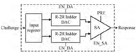
Structure of DAC-PUF.
SEMICONDUCTOR INTEGRATED CIRCUITS
Pengjun Wang, Xuelong Zhang, Yuejun Zhang and Jianrui Li
Corresponding author: Pengjun Wang, E-mail: wangpengjun@nbu.edu.cn
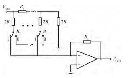
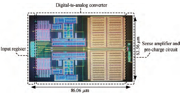
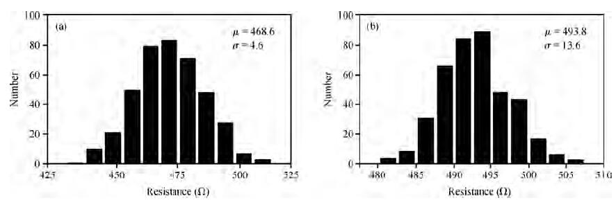
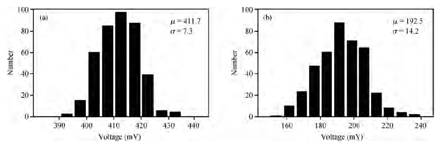
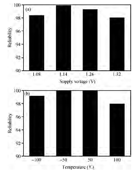
Abstract: A novel physical unclonable functions (PUF) circuit is proposed, which relies on non-linear characteristic of analog voltage generated by R-2R ladder DAC. After amplifying the deviation signal, the robustness of the DAC-PUF circuit has increased significantly. The DAC-PUF circuit is designed in TSMC 65 nm CMOS technology and the layout occupies 86.06 × 63.56 μm2. Monte Carlo simulation results show that the reliability of the DAC-PUF circuit is above 98% over a comprehensive range of environmental variation, such as temperature and supply voltage.
Keywords: process variation, digital-to-analog convertor, physical unclonable functions, sense amplifier
| [1] | |
| [2] | |
| [3] | |
| [4] | |
| [5] | |
| [6] | |
| [7] | |
| [8] | |
| [9] | |
| [10] | |
| [11] |
| [1] | |
| [2] | |
| [3] | |
| [4] | |
| [5] | |
| [6] | |
| [7] | |
| [8] | |
| [9] | |
| [10] | |
| [11] |


Article views: 3328 Times PDF downloads: 29 Times Cited by: 0 Times
Received: 17 November 2014 Revised: Online: Published: 01 July 2015
| Citation: |
Pengjun Wang, Xuelong Zhang, Yuejun Zhang, Jianrui Li. Design of a reliable PUF circuit based on R-2R ladder digital-to-analog convertor[J]. Journal of Semiconductors, 2015, 36(7): 075005. doi: 10.1088/1674-4926/36/7/075005
****
P J Wang, X L Zhang, Y J Zhang, J R Li. Design of a reliable PUF circuit based on R-2R ladder digital-to-analog convertor[J]. J. Semicond., 2015, 36(7): 075005. doi: 10.1088/1674-4926/36/7/075005.

|
| [1] | |
| [2] | |
| [3] | |
| [4] | |
| [5] | |
| [6] | |
| [7] | |
| [8] | |
| [9] | |
| [10] | |
| [11] |

 WeChat ID
Journal of Semiconductors © 2017 All Rights Reserved 京ICP备05085259号-2

 DownLoad: