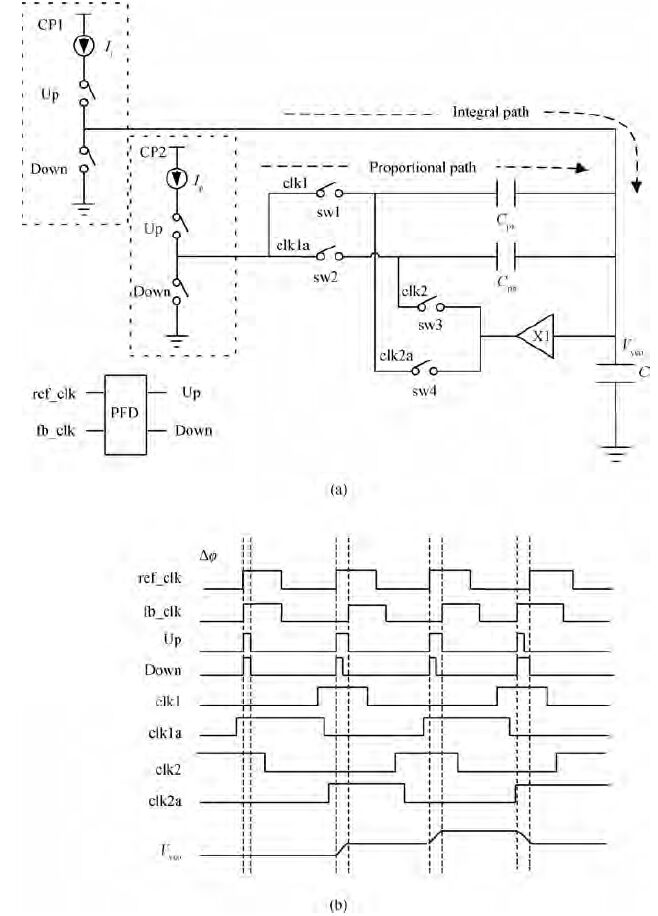
Fig1.
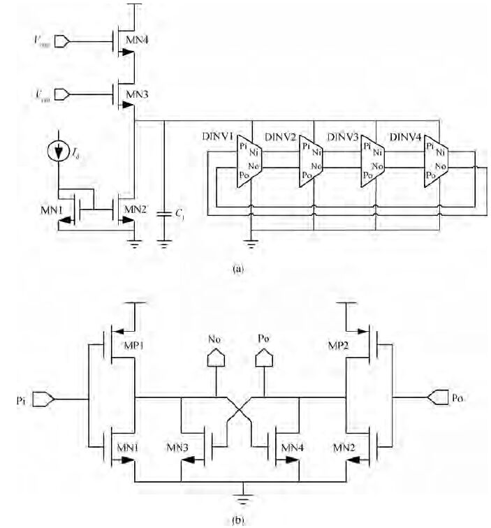
CP and LPF with dual paths. (a) Scheme. (b) Clock sequence and $V_{\rm vco}$ response.
SEMICONDUCTOR INTEGRATED CIRCUITS
Corresponding author: Corresponding author. Email: zhongbo1127@163.com
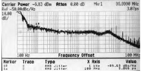
Abstract: A 0.1-1.5 GHz, 3.07 pS root mean squares (RMS) jitter, area efficient phase locked loop (PLL) with multiphase clock outputs is presented in this paper. The size of capacitor in the low pass filter (LPF) is significantly decreased by implementing a dual path charge pump (CP) technique in this PLL. Subject to specified power consumption, a novel optimization method is introduced to optimize the transistor size in the voltage control oscillator (VCO), CP and phase/frequency detector (PFD) in order to minimize clock jitter. This method could improve 3-6 dBc/Hz phase noise. The proposed PLL has been fabricated in 55 nm CMOS process with an integrated 16 pF metal-oxide-metal (MOM) capacitor, occupies 0.05 mm2 silicon area, the measured total power consumption is 2.8 mW @ 1.5 GHz and the phase noise is -102 dBc/Hz @ 1 MHz offset frequency.
Keywords: phase lock loop, freqency synthesizer, dual path charge pump, CMOS
| [1] | |
| [2] | |
| [3] | |
| [4] | |
| [5] | |
| [6] | |
| [7] | |
| [8] | |
| [9] | |
| [10] | |
| [11] | |
| [12] | |
| [13] | |
| [14] | |
| [15] | |
| [16] | |
| [17] | |
| [18] | |
| [19] | |
| [20] | |
| [21] | |
| [22] | |
| [23] | |
| [24] | |
| [25] |
| [1] | |
| [2] | |
| [3] | |
| [4] | |
| [5] | |
| [6] | |
| [7] | |
| [8] | |
| [9] | |
| [10] | |
| [11] | |
| [12] | |
| [13] | |
| [14] | |
| [15] | |
| [16] | |
| [17] | |
| [18] | |
| [19] | |
| [20] | |
| [21] | |
| [22] | |
| [23] | |
| [24] | |
| [25] |


Article views: 3747 Times PDF downloads: 70 Times Cited by: 0 Times
Received: 26 August 2015 Revised: Online: Published: 01 May 2016
| Citation: |
Bo Zhong, Zhangming Zhu. A 0.1-1.5 GHz, low jitter, area efficient PLL in 55-nm CMOS process[J]. Journal of Semiconductors, 2016, 37(5): 055004. doi: 10.1088/1674-4926/37/5/055004
****
B Zhong, Z M Zhu. A 0.1-1.5 GHz, low jitter, area efficient PLL in 55-nm CMOS process[J]. J. Semicond., 2016, 37(5): 055004. doi: 10.1088/1674-4926/37/5/055004.

|
| [1] | |
| [2] | |
| [3] | |
| [4] | |
| [5] | |
| [6] | |
| [7] | |
| [8] | |
| [9] | |
| [10] | |
| [11] | |
| [12] | |
| [13] | |
| [14] | |
| [15] | |
| [16] | |
| [17] | |
| [18] | |
| [19] | |
| [20] | |
| [21] | |
| [22] | |
| [23] | |
| [24] | |
| [25] |

 WeChat ID
Journal of Semiconductors © 2017 All Rights Reserved 京ICP备05085259号-2

 DownLoad: