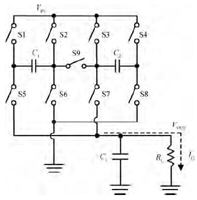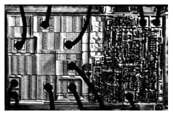
Fig. 1.
Simplified structure of current mode charge pump.
SEMICONDUCTOR INTEGRATED CIRCUITS
Cong Liu1, 2, , Xinquan Lai1, 2, Hanxiao Du1, 2 and Yuan Chi1, 2
Corresponding author: Cong Liu, Email: liucong4213@163.com
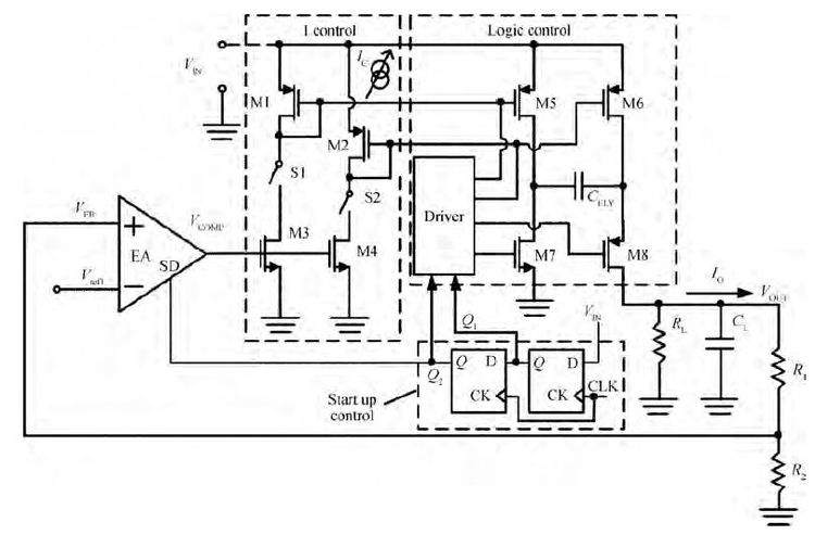
Abstract: A double-stage start-up structure to limit the inrush current used in current-mode charge pump with wide input range, fixed output and multimode operation is presented in this paper. As a widely utilized power source implement, a Li-battery is always used as the power supply for chips. Due to the internal resistance, a potential drop will be generated at the input terminal of the chip with an input current. A false shut down with a low supply voltage will happen if the input current is too large, leading to the degradation of the Li-battery's service life. To solve this problem, the inrush current is limited by introducing a new start-up state. All of the circuits have been implemented with the NUVOTON 0.6 μm CMOS process. The measurement results show that the inrush current can be limited below 1 A within all input supply ranges, and the power efficiency is higher than the conventional structure.
Keywords: charge pump, current mode, inrush current, multimode operation, double-stage start-up
| [1] |
Cabrini A, Fantini A, Torelli G. High-efficiency regulator for on-chip charge pump voltage elevators. Electron Lett, 2006, 42(17):972
|
| [2] |
Wu C, Chen C. High-efficiency current-regulated charge pump for a white LED driver. IEEE Trans Circuits Syst Ⅱ, 2009, 56(10):763
|
| [3] |
Hwu K, Peng T. High-voltage-boosting converter with charge pump capacitor and coupling inductor combined with buck-boost converter. IET Power Electronics, 2014, 7(1):177
|
| [4] |
Zheng C, Chowdhury I, Ma D. Low-noise switched-capacitor power converter with adaptive on-chip surge suppression and pre-emptive timing control. IEEE Trans Power Electron, 2013, 28(11):5174
|
| [5] |
Sittisak C, Jirawath P. Low swing CMOS current mode charge pump. ICCAS, 2010 Int Conf, Gyeonggi-do, Korea (South), Oct 2010:1383
|
| [6] |
Lin R, Shih H. Piezoelectric transformer based current-source charge-pump power-factor-correction electronic ballast. IEEE Trans Power Electron, 2008, 23(3):1391
|
| [7] |
Hsieh Z, Huang N, Shiau M, et al. A novel mixed-structure design for high-efficiency charge pump. MIXDES-16th Int Conf, Lodz, Poland, June 2009:210
|
| [8] |
Yu W, Hutchens C, Lai J, et al. High efficiency converter with charge pump and coupled inductor for wide input photovoltaic AC module applications. ECCE 2009 IEEE, San Jose, USA, Sept 2009:3895
|
| [9] |
Tseng H T, Chen J F. Voltage compensation-type inrush current limiter for reducing power transformer inrush current. IET Electric Power Appl, 2012, 6(2):101
|
| [10] |
Wang X, Sun Y, Li T, et al. Active closed-loop gate voltage control method to mitigate metal oxide semiconductor field-effect transistor turn-off voltage overshoot and ring. IET Power Electron, 2013, 6(8):1715
|
| [11] |
Tsang C, Foster M, Stone D. Active current ripple cancellation in parallel connected buck converter modules. IET Power Electron, 2013, 6(4):721
|
| [12] |
Kuperman A, Aharon I, Malki S, et al. Design of a semiactive battery-ultracapacitor hybrid energy source. IEEE Trans Power Electron, 2013, 28(2):806
|
| [13] |
Yu W, Lai J. Ultra high efficiency bidirectional DC-DC converter with multi-frequency pulse width modulation. APEC 2008 Twenty-Third Annual IEEE, Austin, USA, Feb. 2008:1079
|
| [14] |
Honggang S, Fei W. A fault detection and protection scheme for three-level DC-DC converters based on monitoring flying capacitor voltage. IEEE Trans Power Electron, 2012, 27(2):685
|
| [15] |
Saiz-Vela A, Miribel P, Colomer J. Ripple reduction on skipping-based regulated two-phase voltage doubler charge pump. Electron Lett, 2009, 45(20):1050
|
| [16] |
Yuan B, Lai X. On-chip CMOS current-sensing circuit for DC-DC buck convertor. Electron Lett, 2009, 14(2):102
|
| [17] |
Mohammad M G, Ahmad M J, AI-Bakheet M B. Switched positive/negative charge pump design using standard CMOS transistors. IET Circuits Devices Systems, 2010, 4(1):57
|
| [18] |
Jyoti G, Ankur S, Hemlata V. High speed CMOS charge pump circuit for PLL applications using 90 nm CMOS technology. WICT 2011 World Conf, Mumbai, India, Dec. 2011:346
|
| [19] |
Marcos P, Pfitscher L, Lopes L, et al. Voltage multiplier cells applied to non-isolated DC-DC converters. IEEE Trans Power Electron, 2008, 23(2):871
|
| [20] |
Nuvoton Corp. 0.6μm CMOS process, accessed Dec. 2012 https://download.nuvoton.com/NuvotonMoss/DownloadService/member/DownloadPages.aspx
|
| [21] |
Cheng K W, Divakar B P, Wu H, et al. Battery-management system (BMS) and SOC development for electrical vehicles. IEEE Trans Vehicle Technology, 2011, 60(1):76
|
| [22] |
Antoni S, Chang Y. Battery management system based on battery nonlinear dynamics modeling. IEEE Trans Vehicle Technol, 2008, 57(3):1425
|
| [23] |
Thiele G, Bayer E. Voltage double/tripler current-mode charge pump topology with simple "gear box". PESC 2007 IEEE, Orlando, USA, June 2007:2348
|
| [24] |
Bill R, David P K, Calbert L P. Method and apparatus for a charge pump DC-to-DC converter having parallel operating modes. United States Patent, US7808220B2, 2010
|
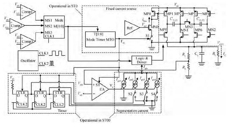
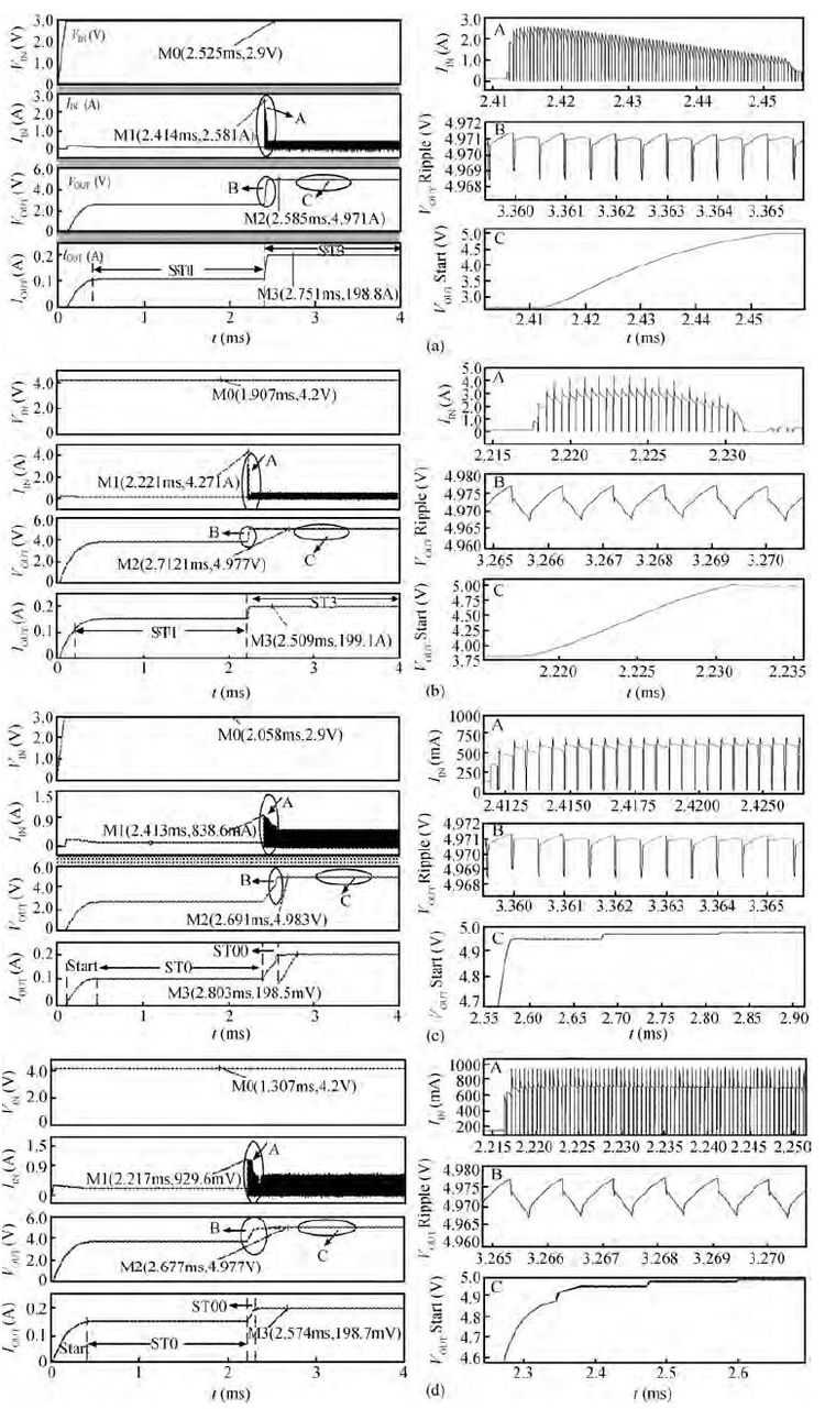
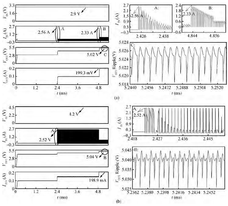
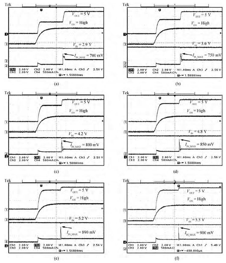
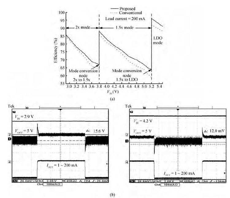
Table 1. Circuit status of each step.
| Component | Step 1 | Step 2 | Step 3 |
| S1 | Open | Closed | Closed |
| S2 | Closed | Open | Closed |
| M5 | Off | On | Off |
| M6 | On | Off | Off |
| M7 | On | Off | Off |
| M8 | Off | On | Off |
 DownLoad: CSV
Table 2. Simulation Conditions.
| Parameter | Value |
| VIN | 2.9 V/4.2 V |
| VOUT | 5 V |
| IO | 200 mA |
| CFLT1 | 1 μF |
| CFLT2 | 1 μF |
| CL | 10 μF |
| W/L\rm PM0 | 300 μm/1 μm |
| W/L\rm NM0 | 10 μm/1 μm |
| W/L\rm PM1 | 30000 μm /1 μm |
| W/L\rm PM2 | 30000 μm /1 μm |
| W/L\rm PM3 | 30000 μm /1 μm |
| W/L\rm PM4 | 30000 μm /1 μm |
| W/L\rm PM5 | 30000 μm /1 μm |
| W/L\rm PM6 | 30000 μm /1 μm |
| W/L\rm NM1 | 15000 μm /1 μm |
| W/L\rm NM2 | 15000 μm /1 μm |
| W/L\rm NM3 | 15000 μm /1 μm |
DownLoad: CSV
Table 3. Summary of the simulation results.
| Output voltage (V) | Output ripple (mV) | Inrush current (A) | Output current (mA) | |
| Conventional | 4.97 @ VIN=2.9 V 4.97 @ VIN = 4.2 V | 3 @ VIN = 2.9 V 11 @ VIN = 4.2 V | 2.593 @ VIN = 2.9 V 4.271 @ VIN = 4.2 V | 200 @ VIN = 2.9 V 200 @ VIN = 4.2 V |
| The widely used chip | 5.02 @ VIN = 2.9 V 5.04 @ VIN = 4.2 V | 8 @ VIN = 2.9 V 18 @ VIN = 4.2 V | 2.560 @ VIN = 2.9 V 2.520 @ VIN = 4.2 V | 200 @ VIN = 2.9 V 200 @ VIN = 4.2 V |
| Proposed | 4.97 @ VIN = 2.9 V 4.97 @ VIN = 4.2 V | 3 @ Vin = 2.9 V 11 @ Vin = 4.2 V | 0.839 @ VIN = 2.9 V 0.929 @ VIN = 4.2 V | 200 @ VIN = 2.9 V 200 @ VIN = 4.2 V |
DownLoad: CSV
Table 4. Performance comparison between the measurement results.
| Item | Proposed chip | Widely used chip |
| Flying capacitor (μF) | 11 | |
| Load capacitor (μF) | 10 | 10 |
| Switching frequency (MHz) | 1 | 1.2 |
| Input voltage range (V) | 2.9-5.5 | 2.9-5.5 |
| Output voltage (V) | 5 | 5 |
| Load current (mA) | 200 | 250 |
| Battery internal resistance (mΩ) | 200 | 200 |
| Inrush current (A) | 0.70 @VIN=2.9 V 0.75 @ VIN=3.6 V 0.80 @ VIN=4.2 V 0.85 @ VIN=4.8 V 0.89 @ VIN=5.2 V 0.90 @ VIN=5.5 V | 2.56 @ VIN=2.9 V 2.55 @ VIN=3.6 V 2.52 @ VIN=4.2 V 2.50 @ VIN=4.8 V 2.45 @ VIN=5.2 V 2.33 @ VIN=5.5 V |
| Startup time (ms) | 2.5 | 1 |
| Load regulation (mV) | 15.6 @ Vin=2.9 V 12.0 @ Vin=4.2 V | 23.9 @ VIN=2.9 V 16.2 @ VIN=4.2 V |
| Maximum efficiency (%) | 86 @ 2x mode 88 @ 1.5x mode 96 @ LDO mode | 85 @ 2x mode 85 @ 1.5x mode 92 @ LDO mode |
DownLoad: CSV
| [1] |
Cabrini A, Fantini A, Torelli G. High-efficiency regulator for on-chip charge pump voltage elevators. Electron Lett, 2006, 42(17):972
|
| [2] |
Wu C, Chen C. High-efficiency current-regulated charge pump for a white LED driver. IEEE Trans Circuits Syst Ⅱ, 2009, 56(10):763
|
| [3] |
Hwu K, Peng T. High-voltage-boosting converter with charge pump capacitor and coupling inductor combined with buck-boost converter. IET Power Electronics, 2014, 7(1):177
|
| [4] |
Zheng C, Chowdhury I, Ma D. Low-noise switched-capacitor power converter with adaptive on-chip surge suppression and pre-emptive timing control. IEEE Trans Power Electron, 2013, 28(11):5174
|
| [5] |
Sittisak C, Jirawath P. Low swing CMOS current mode charge pump. ICCAS, 2010 Int Conf, Gyeonggi-do, Korea (South), Oct 2010:1383
|
| [6] |
Lin R, Shih H. Piezoelectric transformer based current-source charge-pump power-factor-correction electronic ballast. IEEE Trans Power Electron, 2008, 23(3):1391
|
| [7] |
Hsieh Z, Huang N, Shiau M, et al. A novel mixed-structure design for high-efficiency charge pump. MIXDES-16th Int Conf, Lodz, Poland, June 2009:210
|
| [8] |
Yu W, Hutchens C, Lai J, et al. High efficiency converter with charge pump and coupled inductor for wide input photovoltaic AC module applications. ECCE 2009 IEEE, San Jose, USA, Sept 2009:3895
|
| [9] |
Tseng H T, Chen J F. Voltage compensation-type inrush current limiter for reducing power transformer inrush current. IET Electric Power Appl, 2012, 6(2):101
|
| [10] |
Wang X, Sun Y, Li T, et al. Active closed-loop gate voltage control method to mitigate metal oxide semiconductor field-effect transistor turn-off voltage overshoot and ring. IET Power Electron, 2013, 6(8):1715
|
| [11] |
Tsang C, Foster M, Stone D. Active current ripple cancellation in parallel connected buck converter modules. IET Power Electron, 2013, 6(4):721
|
| [12] |
Kuperman A, Aharon I, Malki S, et al. Design of a semiactive battery-ultracapacitor hybrid energy source. IEEE Trans Power Electron, 2013, 28(2):806
|
| [13] |
Yu W, Lai J. Ultra high efficiency bidirectional DC-DC converter with multi-frequency pulse width modulation. APEC 2008 Twenty-Third Annual IEEE, Austin, USA, Feb. 2008:1079
|
| [14] |
Honggang S, Fei W. A fault detection and protection scheme for three-level DC-DC converters based on monitoring flying capacitor voltage. IEEE Trans Power Electron, 2012, 27(2):685
|
| [15] |
Saiz-Vela A, Miribel P, Colomer J. Ripple reduction on skipping-based regulated two-phase voltage doubler charge pump. Electron Lett, 2009, 45(20):1050
|
| [16] |
Yuan B, Lai X. On-chip CMOS current-sensing circuit for DC-DC buck convertor. Electron Lett, 2009, 14(2):102
|
| [17] |
Mohammad M G, Ahmad M J, AI-Bakheet M B. Switched positive/negative charge pump design using standard CMOS transistors. IET Circuits Devices Systems, 2010, 4(1):57
|
| [18] |
Jyoti G, Ankur S, Hemlata V. High speed CMOS charge pump circuit for PLL applications using 90 nm CMOS technology. WICT 2011 World Conf, Mumbai, India, Dec. 2011:346
|
| [19] |
Marcos P, Pfitscher L, Lopes L, et al. Voltage multiplier cells applied to non-isolated DC-DC converters. IEEE Trans Power Electron, 2008, 23(2):871
|
| [20] |
Nuvoton Corp. 0.6μm CMOS process, accessed Dec. 2012 https://download.nuvoton.com/NuvotonMoss/DownloadService/member/DownloadPages.aspx
|
| [21] |
Cheng K W, Divakar B P, Wu H, et al. Battery-management system (BMS) and SOC development for electrical vehicles. IEEE Trans Vehicle Technology, 2011, 60(1):76
|
| [22] |
Antoni S, Chang Y. Battery management system based on battery nonlinear dynamics modeling. IEEE Trans Vehicle Technol, 2008, 57(3):1425
|
| [23] |
Thiele G, Bayer E. Voltage double/tripler current-mode charge pump topology with simple "gear box". PESC 2007 IEEE, Orlando, USA, June 2007:2348
|
| [24] |
Bill R, David P K, Calbert L P. Method and apparatus for a charge pump DC-to-DC converter having parallel operating modes. United States Patent, US7808220B2, 2010
|


Article views: 4732 Times PDF downloads: 44 Times Cited by: 0 Times
Received: 16 September 2015 Revised: 03 November 2015 Online: Published: 01 June 2016
| Citation: |
Cong Liu, Xinquan Lai, Hanxiao Du, Yuan Chi. A double-stage start-up structure to limit the inrush current used in current mode charge pump[J]. Journal of Semiconductors, 2016, 37(6): 065006. doi: 10.1088/1674-4926/37/6/065006
****
C Liu, X Q Lai, H X Du, Y Chi. A double-stage start-up structure to limit the inrush current used in current mode charge pump[J]. J. Semicond., 2016, 37(6): 065006. doi: 10.1088/1674-4926/37/6/065006.

|
| [1] |
Cabrini A, Fantini A, Torelli G. High-efficiency regulator for on-chip charge pump voltage elevators. Electron Lett, 2006, 42(17):972
|
| [2] |
Wu C, Chen C. High-efficiency current-regulated charge pump for a white LED driver. IEEE Trans Circuits Syst Ⅱ, 2009, 56(10):763
|
| [3] |
Hwu K, Peng T. High-voltage-boosting converter with charge pump capacitor and coupling inductor combined with buck-boost converter. IET Power Electronics, 2014, 7(1):177
|
| [4] |
Zheng C, Chowdhury I, Ma D. Low-noise switched-capacitor power converter with adaptive on-chip surge suppression and pre-emptive timing control. IEEE Trans Power Electron, 2013, 28(11):5174
|
| [5] |
Sittisak C, Jirawath P. Low swing CMOS current mode charge pump. ICCAS, 2010 Int Conf, Gyeonggi-do, Korea (South), Oct 2010:1383
|
| [6] |
Lin R, Shih H. Piezoelectric transformer based current-source charge-pump power-factor-correction electronic ballast. IEEE Trans Power Electron, 2008, 23(3):1391
|
| [7] |
Hsieh Z, Huang N, Shiau M, et al. A novel mixed-structure design for high-efficiency charge pump. MIXDES-16th Int Conf, Lodz, Poland, June 2009:210
|
| [8] |
Yu W, Hutchens C, Lai J, et al. High efficiency converter with charge pump and coupled inductor for wide input photovoltaic AC module applications. ECCE 2009 IEEE, San Jose, USA, Sept 2009:3895
|
| [9] |
Tseng H T, Chen J F. Voltage compensation-type inrush current limiter for reducing power transformer inrush current. IET Electric Power Appl, 2012, 6(2):101
|
| [10] |
Wang X, Sun Y, Li T, et al. Active closed-loop gate voltage control method to mitigate metal oxide semiconductor field-effect transistor turn-off voltage overshoot and ring. IET Power Electron, 2013, 6(8):1715
|
| [11] |
Tsang C, Foster M, Stone D. Active current ripple cancellation in parallel connected buck converter modules. IET Power Electron, 2013, 6(4):721
|
| [12] |
Kuperman A, Aharon I, Malki S, et al. Design of a semiactive battery-ultracapacitor hybrid energy source. IEEE Trans Power Electron, 2013, 28(2):806
|
| [13] |
Yu W, Lai J. Ultra high efficiency bidirectional DC-DC converter with multi-frequency pulse width modulation. APEC 2008 Twenty-Third Annual IEEE, Austin, USA, Feb. 2008:1079
|
| [14] |
Honggang S, Fei W. A fault detection and protection scheme for three-level DC-DC converters based on monitoring flying capacitor voltage. IEEE Trans Power Electron, 2012, 27(2):685
|
| [15] |
Saiz-Vela A, Miribel P, Colomer J. Ripple reduction on skipping-based regulated two-phase voltage doubler charge pump. Electron Lett, 2009, 45(20):1050
|
| [16] |
Yuan B, Lai X. On-chip CMOS current-sensing circuit for DC-DC buck convertor. Electron Lett, 2009, 14(2):102
|
| [17] |
Mohammad M G, Ahmad M J, AI-Bakheet M B. Switched positive/negative charge pump design using standard CMOS transistors. IET Circuits Devices Systems, 2010, 4(1):57
|
| [18] |
Jyoti G, Ankur S, Hemlata V. High speed CMOS charge pump circuit for PLL applications using 90 nm CMOS technology. WICT 2011 World Conf, Mumbai, India, Dec. 2011:346
|
| [19] |
Marcos P, Pfitscher L, Lopes L, et al. Voltage multiplier cells applied to non-isolated DC-DC converters. IEEE Trans Power Electron, 2008, 23(2):871
|
| [20] |
Nuvoton Corp. 0.6μm CMOS process, accessed Dec. 2012 https://download.nuvoton.com/NuvotonMoss/DownloadService/member/DownloadPages.aspx
|
| [21] |
Cheng K W, Divakar B P, Wu H, et al. Battery-management system (BMS) and SOC development for electrical vehicles. IEEE Trans Vehicle Technology, 2011, 60(1):76
|
| [22] |
Antoni S, Chang Y. Battery management system based on battery nonlinear dynamics modeling. IEEE Trans Vehicle Technol, 2008, 57(3):1425
|
| [23] |
Thiele G, Bayer E. Voltage double/tripler current-mode charge pump topology with simple "gear box". PESC 2007 IEEE, Orlando, USA, June 2007:2348
|
| [24] |
Bill R, David P K, Calbert L P. Method and apparatus for a charge pump DC-to-DC converter having parallel operating modes. United States Patent, US7808220B2, 2010
|

 WeChat ID
Journal of Semiconductors © 2017 All Rights Reserved 京ICP备05085259号-2