


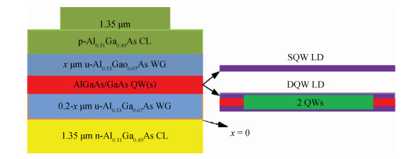
Fig. 1.
(Color online) Schematic diagram of SQW and DQW LD structure.
SEMICONDUCTOR DEVICES
Yi Pang, Xiang Li and Baiqin Zhao
Corresponding author: Pang Yi, Email: madaog@sina.cn
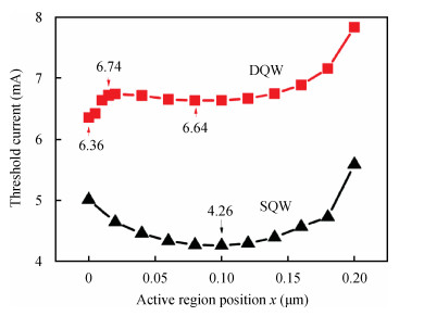
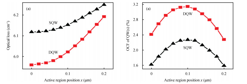
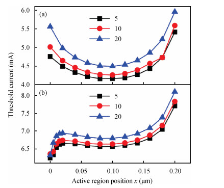
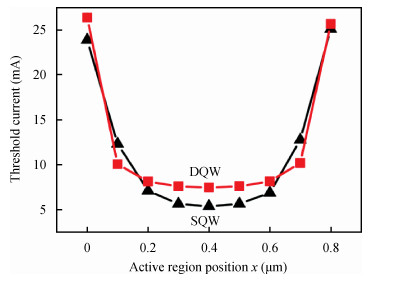
Abstract: The paper mainly deals with theoretical investigations of the effect of the thickness change of the waveguide layers on the threshold current. It is analyzed according to the result of a numerical simulation that asks how does the shift of the active region position affect the threshold current for a single quantum well (SQW) and double quantum well (DQW) laser diode (LD) with a relatively narrow waveguide. It is found that the variation trend of threshold current and optimum position of QW are different in SQW and DQW LD with 0.2 μm-thick waveguide, which may be due to the higher variation rate of optical loss in DQW LD with the shift of the active region. It is also found that in terms of either SQW or DQW LD, the variation tendency of the threshold current with a different loss coefficient of the p-cladding layer makes little difference for the relatively narrow waveguide LD. Moreover, the variation trend of the threshold current and the optimum position of QW is almost the same in SQW and DQW LD with 0.8μm-thick waveguide, because the optical loss is small enough and the threshold current is dominated by the optical confinement factor (OCF) in QW.
Keywords: semiconductor, laser diode, threshold current, simulation
| [1] |
Zhu Zhen, Zhang Xin, Li Peixu, et al. Voltage reduction of 808 nm GaAsP/(Al)GaInP laser diodes with GaInAsP intermediate layer. Journal of Semiconductors, 2015, 36(1): 014011 doi: 10.1088/1674-4926/36/1/014011
|
| [2] |
Li Xiang, Zhao Degang, Jiang Desheng, et al. Fabrication of ridge waveguide of 808 nm GaAs-based laser diodes by wet chemical etching. Journal of Semiconductors, 2015, 36(7): 074009 doi: 10.1088/1674-4926/36/7/074009
|
| [3] |
Wang Yong, Liu Dandan, Feng Guoqing, et al. Preparation for Bragg grating of 808 nm distributed feedback laser diode. Journal of Semiconductors, 2015, 36(5): 054008 doi: 10.1088/1674-4926/36/5/054008
|
| [4] |
Li X, Zhao D G, Jiang D S, et al. A modified structure with asymmetric and doping barrier interlayers of GaAs-based laser diodes with both small vertical divergence angle and low threshold current. Superlattices and Microstructures, 2015, 80:111 doi: 10.1016/j.spmi.2015.01.006
|
| [5] |
Gilor J, Samid I, Fekete D. Threshold current density reduction of strained AlInGaAs quantum-well laser. IEEE J Quantum Electron, 2004, 40(10):1355 doi: 10.1109/JQE.2004.834561
|
| [6] |
Wang Huolei, Yu Hongyan, Zhou Xuliang, et al. High-power InGaAs/GaAs quantum-well laser with enhanced broad spectrum of stimulated emission. Appl Phys Lett, 2014, 105(14): 141101 doi: 10.1063/1.4897436
|
| [7] |
Lee J J, Mawst L J, Botez D. Asymmetric broad waveguide diode lasers (λ=980 nm) of large equivalent transverse spot size and low temperature sensitivity. Photonics Technol Lett, 2002, 14(8): 1046 doi: 10.1109/LPT.2002.1021964
|
| [8] |
Wenzel H. Basic aspects of high-power semiconductor laser simulation. IEEE J Sel Topics Quantum Electron, 2013, 19(5): 1 http://cn.bing.com/academic/profile?id=2004953461&encoded=0&v=paper_preview&mkt=zh-cn
|
| [9] |
Zhukov A E, Asryan L V, Semenova E S, et al. On the optimization of asymmetric barrier layers in InAlGaAs/AlGaAs laser heterostructures on GaAs substrates. Semi-conductors on GaAs substrates. Semiconductors, 2015, 49(7): 935 doi: 10.1134/S1063782615070258
|
| [10] |
Fan D S, Grant P C, Yu S Q, et al. MBE grown GaAsBi/GaAs double quantum well separate confinement heterostructures. J Vac Sci Technol B, 2013, 31(3): 03C105 http://cn.bing.com/academic/profile?id=2063600703&encoded=0&v=paper_preview&mkt=zh-cn
|
| [11] |
Alvi P A, Lal P, Yadav R, et al. Modal gain characteristics of GRIN-InGaAlAs/InP lasing nano-heterostructures. Supetlattice Microst, 2013, 61: 1 doi: 10.1016/j.spmi.2013.05.019
|
| [12] |
www.crosslight.com for LASTIP by Crosslight Software Inc
|
| [13] |
Nawaz M, Permthamassin K, Zaring C, et al. A theoretical optimization of GaInP/GaInAs/GaAs based 980 nm Al-free pump laser using self-consistent numerical simulation. Solid-State Electron, 2001, 47(2): 289 http://cn.bing.com/academic/profile?id=2177927605&encoded=0&v=paper_preview&mkt=zh-cn
|
| [14] |
Yen Shenghorng, Chen Meiling, Kuo Yenkuang. Gain and threshold properties of InGaAsN/GaAsN material system for 1.3-μm semiconductor lasers. Optics & Laser Technol, 2007, 39(7): 1432 http://cn.bing.com/academic/profile?id=2008678283&encoded=0&v=paper_preview&mkt=zh-cn
|
| [15] |
Kopf R F, Herman M H, Schnoes M L. Band offset determination in analog graded parabolic and triangular quantum wells of GaAs/AlGaAs and GaInAs/AlInAs. J Appl Phys, 1992, 71(10): 5004 doi: 10.1063/1.350600
|
| [16] |
Gokhale M R, Dries J C, Studenkov P V, et al. High-power high-efficiency 0.98-μm wavelength InGaAs-(In)GaAs(P)-InGaP broaded waveguide lasers grown by gas-source molecular beam epitaxy. IEEE J Quantum Electron, 1997, 33(12): 2266 doi: 10.1109/3.644109
|
| [17] |
Slipchenko S O, Vinokurov D A, Pikhtin N A, et al. Ultralow internal optical loss in separate-confinement quantum-well laser heterostructures. Semiconductors, 2004, 38(12): 1430 doi: 10.1134/1.1836066
|
| [18] |
Ryvkin B S, Avrutin E A. Asymmetric, nonbroadened large optical cavity waveguide structures for high-power long-wavelength semiconductor lasers. J Appl Phys, 2005, 97(12): 123103 doi: 10.1063/1.1928309
|
| [19] |
Ryvkin B S, Avrutin E A. Improvement of differential quantum efficiency and power output by waveguide asymmetry in separate-confinement-structure diode lasers. IEEE Proc Optoelectron, 2004, 151(4): 232 doi: 10.1049/ip-opt:20040633
|


Article views: 3752 Times PDF downloads: 26 Times Cited by: 0 Times
Received: 05 January 2016 Revised: 29 February 2016 Online: Published: 01 August 2016
| Citation: |
Yi Pang, Xiang Li, Baiqin Zhao. Influence of the thickness change of the wave-guide layers on the threshold current of GaAs-based laser diode[J]. Journal of Semiconductors, 2016, 37(8): 084007. doi: 10.1088/1674-4926/37/8/084007
****
Y Pang, X Li, B Q Zhao. Influence of the thickness change of the wave-guide layers on the threshold current of GaAs-based laser diode[J]. J. Semicond., 2016, 37(8): 084007. doi: 10.1088/1674-4926/37/8/084007.

|
| [1] |
Zhu Zhen, Zhang Xin, Li Peixu, et al. Voltage reduction of 808 nm GaAsP/(Al)GaInP laser diodes with GaInAsP intermediate layer. Journal of Semiconductors, 2015, 36(1): 014011 doi: 10.1088/1674-4926/36/1/014011
|
| [2] |
Li Xiang, Zhao Degang, Jiang Desheng, et al. Fabrication of ridge waveguide of 808 nm GaAs-based laser diodes by wet chemical etching. Journal of Semiconductors, 2015, 36(7): 074009 doi: 10.1088/1674-4926/36/7/074009
|
| [3] |
Wang Yong, Liu Dandan, Feng Guoqing, et al. Preparation for Bragg grating of 808 nm distributed feedback laser diode. Journal of Semiconductors, 2015, 36(5): 054008 doi: 10.1088/1674-4926/36/5/054008
|
| [4] |
Li X, Zhao D G, Jiang D S, et al. A modified structure with asymmetric and doping barrier interlayers of GaAs-based laser diodes with both small vertical divergence angle and low threshold current. Superlattices and Microstructures, 2015, 80:111 doi: 10.1016/j.spmi.2015.01.006
|
| [5] |
Gilor J, Samid I, Fekete D. Threshold current density reduction of strained AlInGaAs quantum-well laser. IEEE J Quantum Electron, 2004, 40(10):1355 doi: 10.1109/JQE.2004.834561
|
| [6] |
Wang Huolei, Yu Hongyan, Zhou Xuliang, et al. High-power InGaAs/GaAs quantum-well laser with enhanced broad spectrum of stimulated emission. Appl Phys Lett, 2014, 105(14): 141101 doi: 10.1063/1.4897436
|
| [7] |
Lee J J, Mawst L J, Botez D. Asymmetric broad waveguide diode lasers (λ=980 nm) of large equivalent transverse spot size and low temperature sensitivity. Photonics Technol Lett, 2002, 14(8): 1046 doi: 10.1109/LPT.2002.1021964
|
| [8] |
Wenzel H. Basic aspects of high-power semiconductor laser simulation. IEEE J Sel Topics Quantum Electron, 2013, 19(5): 1 http://cn.bing.com/academic/profile?id=2004953461&encoded=0&v=paper_preview&mkt=zh-cn
|
| [9] |
Zhukov A E, Asryan L V, Semenova E S, et al. On the optimization of asymmetric barrier layers in InAlGaAs/AlGaAs laser heterostructures on GaAs substrates. Semi-conductors on GaAs substrates. Semiconductors, 2015, 49(7): 935 doi: 10.1134/S1063782615070258
|
| [10] |
Fan D S, Grant P C, Yu S Q, et al. MBE grown GaAsBi/GaAs double quantum well separate confinement heterostructures. J Vac Sci Technol B, 2013, 31(3): 03C105 http://cn.bing.com/academic/profile?id=2063600703&encoded=0&v=paper_preview&mkt=zh-cn
|
| [11] |
Alvi P A, Lal P, Yadav R, et al. Modal gain characteristics of GRIN-InGaAlAs/InP lasing nano-heterostructures. Supetlattice Microst, 2013, 61: 1 doi: 10.1016/j.spmi.2013.05.019
|
| [12] |
www.crosslight.com for LASTIP by Crosslight Software Inc
|
| [13] |
Nawaz M, Permthamassin K, Zaring C, et al. A theoretical optimization of GaInP/GaInAs/GaAs based 980 nm Al-free pump laser using self-consistent numerical simulation. Solid-State Electron, 2001, 47(2): 289 http://cn.bing.com/academic/profile?id=2177927605&encoded=0&v=paper_preview&mkt=zh-cn
|
| [14] |
Yen Shenghorng, Chen Meiling, Kuo Yenkuang. Gain and threshold properties of InGaAsN/GaAsN material system for 1.3-μm semiconductor lasers. Optics & Laser Technol, 2007, 39(7): 1432 http://cn.bing.com/academic/profile?id=2008678283&encoded=0&v=paper_preview&mkt=zh-cn
|
| [15] |
Kopf R F, Herman M H, Schnoes M L. Band offset determination in analog graded parabolic and triangular quantum wells of GaAs/AlGaAs and GaInAs/AlInAs. J Appl Phys, 1992, 71(10): 5004 doi: 10.1063/1.350600
|
| [16] |
Gokhale M R, Dries J C, Studenkov P V, et al. High-power high-efficiency 0.98-μm wavelength InGaAs-(In)GaAs(P)-InGaP broaded waveguide lasers grown by gas-source molecular beam epitaxy. IEEE J Quantum Electron, 1997, 33(12): 2266 doi: 10.1109/3.644109
|
| [17] |
Slipchenko S O, Vinokurov D A, Pikhtin N A, et al. Ultralow internal optical loss in separate-confinement quantum-well laser heterostructures. Semiconductors, 2004, 38(12): 1430 doi: 10.1134/1.1836066
|
| [18] |
Ryvkin B S, Avrutin E A. Asymmetric, nonbroadened large optical cavity waveguide structures for high-power long-wavelength semiconductor lasers. J Appl Phys, 2005, 97(12): 123103 doi: 10.1063/1.1928309
|
| [19] |
Ryvkin B S, Avrutin E A. Improvement of differential quantum efficiency and power output by waveguide asymmetry in separate-confinement-structure diode lasers. IEEE Proc Optoelectron, 2004, 151(4): 232 doi: 10.1049/ip-opt:20040633
|

 WeChat ID
Journal of Semiconductors © 2017 All Rights Reserved 京ICP备05085259号-2

 DownLoad:

