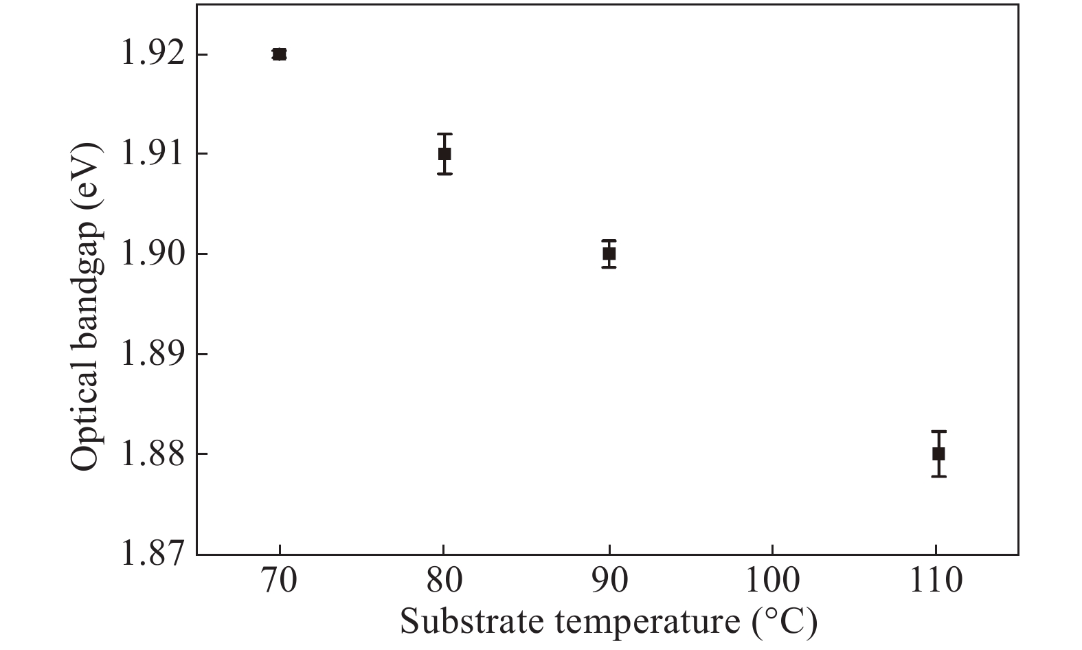
Fig. 1.
Dependence of p-nc-Si:H Eg on substrate temperature.
SEMICONDUCTOR DEVICES
Shuwei Zhang1, 2 and Xiangbo Zeng1, 2,
Corresponding author: Xiangbo Zeng, E-mail address: xbzeng@semi.ac.cn
Abstract: The impact of the optical band gap (Eg) of a p-type hydrogenated nanocrystalline silicon layer on the short-circuit current density (Jsc) of a thin-film silicon solar cell is assessed. We have found that the Jsc reaches maximum when the Eg reaches optimum. The reason for the Jsc on Eg needs to be clarified. Our results exhibit that maximum Jsc is the balance between dark current and photocurrent. We show here that this dark current results from the density of defects in the p-layer and the barrier at the interface between p- and i-layers. An optimum cell can be designed by optimizing the p-layer via reducing the density of defects in the p-layer and the barrier at the p/i interface. Finally, a 6.6% increase in Jsc was obtained at optimum Eg for n–i–p solar cells.
Keywords: nanocrystalline silicon, band gap, p-layer, short-circuit current density, solar cells
| [1] |
Sharma M, Juneja S, Sudhakar S, et al. Optimization of a-Si:H absorber layer grown under a low pressure regime by plasma-enhanced chemical vapor deposition: revisiting the significance of the p/i interface for solar cells. Mater Sci Semicond Process, 2016, 43: 41 doi: 10.1016/j.mssp.2015.10.021
|
| [2] |
Chen X, Liu J, Jia F, et al. High haze textured surface B-doped ZnO-TCO films on wet-chemically etched glass substrates for thin film solar cells. J Semicond, 2016, 37(8): 083003 doi: 10.1088/1674-4926/37/8/083003
|
| [3] |
Tawada Y, Okamoto H, Hamakawa Y. a-SiC:H/a-Si:H heterojunction solar cell having more than 7.1% conversion efficiency. Appln Phys Lett, 1981, 39(3): 237 doi: 10.1063/1.92692
|
| [4] |
Lee Y J, Lee S H, Schropp R E I, et al. Multi-layered hydrogenated p-type microcrystalline silicon windows for a-Si:H thin film solar cells on opaque substrates. Int J Hydrogen Energy, 2016, 41(15): 6240. doi: 10.1016/j.ijhydene.2016.03.011
|
| [5] |
Luque. A, Hegedus S, Handbook of photovoltaic science and engineering. New York: John Wiley & Sons, 2011, 529
|
| [6] |
Tan H, Babal P, Zeman M, et al. Wide bandgap p-type nanocrystalline silicon oxide as window layer for high performance thin-film silicon multi-junction solar cells. Sol Energy Mater Sol Cells, 2015, 132: 597 doi: 10.1016/j.solmat.2014.10.020
|
| [7] |
Ma J, Ni J, Zhang J, et al. Improvement of solar cells performance by boron doped amorphous silicon carbide/nanocrystalline silicon hybrid window layers. Sol Energy Mater Sol Cells, 2013, 114(4): 9
|
| [8] |
Ashida Y. Single-junction a-Si solar cells with over 13% efficiency. Sol Energy Mater Sol Cells, 1994, 34(1-4): 291 doi: 10.1016/0927-0248(94)90053-1
|
| [9] |
Hishida M, Sekimoto T, Terakawa A. Designing band offset of a-SiO:H solar cells for very high open-circuit voltage (1.06 V) by adjusting band gap of p-i-n junction. Jpn J Appl Phys, 2014, 53(9): 092301 doi: 10.7567/JJAP.53.092301
|
| [10] |
Schade H, Smith Z E. Optical properties and quantum efficiency of aSi1-x/C x/:H/aSi:H solar cells. J Appl Phys, 1985, 57(2): 568 doi: 10.1063/1.334739
|
| [11] |
Das D, Kar D. Self-assembled nc-Si-QD/a-SiC thin films from planar ICP-CVD plasma without H2-dilution: a combination of wide optical gap, high conductivity and preferred 〈220〉 crystallographic orientation, uniquely appropriate for nc-Si solar cells. RSC Adva, 2015, 6(5): 3860
|
| [12] |
Liao X, Du W, Yang X, et al. Nanostructure in the p-layer and its impacts on amorphous silicon solar cells. J Non-Cryst Solids, 2006, 352(9-20): 1841 doi: 10.1016/j.jnoncrysol.2005.11.110
|
| [13] |
Koval R J, Chen C, Ferreira G M, et al. Maximization of the open circuit voltage for hydrogenated amorphous silicon n-i-p, solar cells by incorporation of protocrystalline silicon p-type layers. Appln Phys Lett, 2002, 81(7): 1258 doi: 10.1063/1.1499735
|
| [14] |
Guha S, Yang J, Nath P, et al. Enhancement of open circuit voltage in high efficiency amorphous silicon alloy solar cells. Appl Phys Lett, 1986, 49(4): 218 doi: 10.1063/1.97176
|
| [15] |
Vygranenko Y, Fathi E, Sazonov A, et al. Nanocrystalline p-layer for a-Si:H p-i-n solar cells and photodiodes. Sol Energy Mater Sol Cells, 2010, 94(11): 1860 doi: 10.1016/j.solmat.2010.06.044
|
| [16] |
Vasiliev I, Ogut S, Chelikowsky J R. Ab initio absorption spectra and optical gaps in nanocrystalline silicon. Phys Rev Lett, 2001, 86(9):1813 doi: 10.1103/PhysRevLett.86.1813
|
| [17] |
Delley B, Steigmeier E F. Size dependence of band gaps in silicon nanostructures. Appl Phys Lett, 1995, 67(16): 2370 doi: 10.1063/1.114348
|
| [18] |
Delley B, Steigmeier E F. Quantum confinement in Si nanocrystals. Phys Rev B, 1993, 47(3): 1397 doi: 10.1103/PhysRevB.47.1397
|
| [19] |
Polemi A, Alu A, Engheta N. Electronic and structural properties of doped amorphous and nanocrystalline silicon deposited at low substrate temperatures by radio-frequency plasma-enhanced chemical vapor deposition. J Vac Sci Technol A, 2003, 21(4): 1048 doi: 10.1116/1.1586275
|
| [20] |
Yang D, Zhu X, Sun H, et al. Effects of substrate temperature on structural, optical and morphological properties of hydrogenated nanocrystalline silicon thin films prepared by inductively coupled plasma chemical vapor deposition. J Mater Sci: Mater Electron, 2015, 26(10): 7790 doi: 10.1007/s10854-015-3426-0
|
| [21] |
Swanepoel R. Determination of the thickness and optical constants of amorphous silicon. J Phys E, 1983, 16(12): 1214 doi: 10.1088/0022-3735/16/12/023
|
| [22] |
Li Z, Zhang X, Han G. Electrical and optical properties of boron-doped nanocrystalline silicon films deposited by PECVD. Phys Status Solidi Appl Mater, 2010, 207(1): 144 doi: 10.1002/pssa.v207:1
|
| [23] |
Hou G, Fang J, Fan Q H, et al. Nanostructured silicon p-layer obtained by radio frequency power profiling process for high-efficiency amorphous silicon solar cell. Sol Energy Mater Sol Cells, 2015, 134: 395 doi: 10.1016/j.solmat.2014.12.017
|
| [24] |
Liu X, Zi W, Liu S. p-Layer bandgap engineering for high efficiency thin film silicon solar cells. Mater Sci Semicond Process, 2015, 39: 192 doi: 10.1016/j.mssp.2015.04.011
|
| [25] |
Wronski C R, Collins R W. Phase engineering of a-Si:H solar cells for optimized performance. Solar Energy, 2004, 77(6): 877 doi: 10.1016/j.solener.2004.03.008
|
| [26] |
Garrido B, Morante J R, Achiq A, et al. Structural, optical, and electrical properties of nanocrystalline silicon films deposited by hydrogen plasma sputtering. J Vac Sci Technol B, 1998, 16(4): 1851 doi: 10.1116/1.590097
|
| [27] |
Cheng Q, Xu S, Ostrikov K K. Structural evolution of nanocrystalline silicon thin films synthesized in high-density, low-temperature reactive plasmas. Nanotechnology, 2009, 20(21): 215606 doi: 10.1088/0957-4484/20/21/215606
|
| [28] |
Ali A M. Optical properties of nanocrystalline silicon films deposited by plasma-enhanced chemical vapor deposition. Opt Mater, 2007, 30(2): 238 doi: 10.1016/j.optmat.2006.11.042
|
| [29] |
Hegedus S S. Current-voltage analysis of a-Si and a-SiGe solar cells including voltage-dependent photocurrent collection. Prog Photovoltaics Res Appl, 1997, 5(3): 151 doi: 10.1002/(ISSN)1099-159X
|
| [30] |
Matsuda A, Takai M, Nishimoto T, et al. Control of plasma chemistry for preparing highly stabilized amorphous silicon at high growth rate. Sol Energy Mater Sol Cells, 2003, 78(1-4): 3 doi: 10.1016/S0927-0248(02)00431-2
|
| [31] |
Gangyi X, Tianmin W. Electrical characterization of N-type nanocrystalline silicon on p-type crystalline silicon (nc-Si:H/c-Si) heterojunctions. Semicond Sci Technol, 2000, 15(6): 613 doi: 10.1088/0268-1242/15/6/322
|
| [32] |
Fang L, Baik S J, Lim K S, et al. Tungsten oxide as a buffer layer inserted at the SnO2/p-a-SiC interface of pin-type amorphous silicon based solar cells. Appl Phys Lett, 2010, 96(19): 106
|
| [33] |
Belfar A, Aït-Kaci H. Effect of incorporating p-type hydrogenated nanocrystalline silicon buffer layer on amorphous silicon n-i-p solar cell performances. Thin Solid Films, 2012, 525(25): 167
|
| [34] |
Chatterjee P. A computer analysis of the effect of a wide-band-gap emitter layer on the performance of a-Si:H-based heterojunction solar cells. J Appl Phys, 1996, 79(9): 7339 doi: 10.1063/1.361450
|
| [35] |
Hamma S, Roca i C P. Determination of the mobility gap of microcrystalline silicon and of the band discontinuities at the amorphous/microcrystalline silicon interface using in situ Kelvin probe technique. Appl Phys Lett, 1999, 74(21): 3218 doi: 10.1063/1.124110
|
| [36] |
Arch J K, Rubinelli F A, Hou J, et al. Computer analysis of the role of p-layer quality, thickness, transport mechanisms, and contact barrier height in the performance of hydrogenated amorphous silicon p-i-n solar cells. J Appl Phys, 1991, 69(10): 7057 doi: 10.1063/1.347645
|
| [37] |
Cleef M W M V, Schropp R E I, Rubinelli F A. Significance of tunneling in p+ amorphous silicon carbide n crystalline silicon heterojunction solar cells. Appl Phys Lett, 1998, 73(18): 2609 doi: 10.1063/1.122521
|
| [38] |
Liu S, Zeng X, Peng W, et al. Improvement of amorphous silicon n-i-p solar cells by incorporating double-layer hydrogenated nanocrystalline silicon structure. J Non-Cryst Solids, 2011, 357(1): 121 doi: 10.1016/j.jnoncrysol.2010.10.001
|
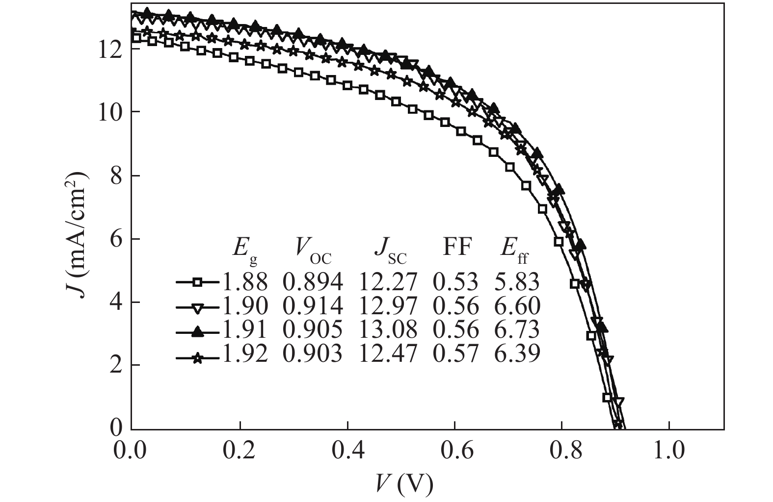
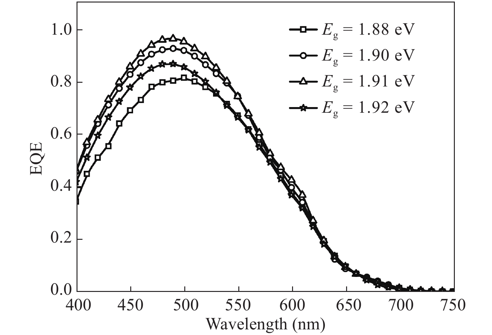
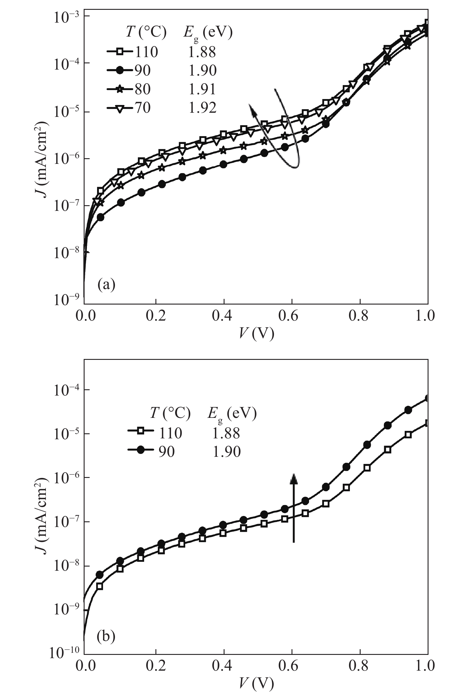
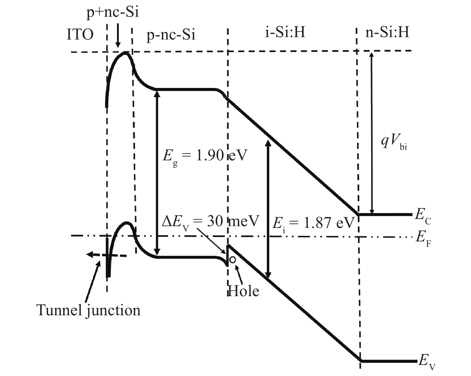
Table 1. Deposition parameters of each layer in single junction Si:H n–i–p solar cells.
| Parameter | n-layer (n-a-Si:H) | i-layer (i-Si:H) | p-layer (p-nc-Si:H) |
| Substrate temperature (°C) | 250 | 220 | 70/80/90/110 |
| Pressure (Pa) | 300 | 133 | 266 |
| Radio frequency (MHZ) | 13.56 | 60 | 13.56 |
| Power (mW/cm2) | 500 | 500 | 1000 |
| Flow rate (sccm) | SiH4 : H2 : PH3(1%) = 3 : 100 : 5 | SiH4 : H2 = 6 : 60 | SiH4 : H2 : B2H6(0.5%) = 1 : 100 : 2 |
 DownLoad: CSV
Table 2. Details of Jsc on Eg among various Si:H solar cells available in literature.
| nc-Si:H[23] | nc-Si:H[24] | nc-Si:H (this work) | |||||
| Eg (eV) | Jsc (mA/cm2) | Eg (eV) | Jsc (mA/cm2) | Eg (eV) | Jsc (mA/cm2) | ||
| 1.82 | 10.40 | 1.85 | 9.50 | 1.88 | 12.27 | ||
| 1.90 | 10.58 | 1.95 | 11.2 | 1.90 | 12.97 | ||
| 1.91 | 10.71 | 1.97 | 10.9 | 1.91 | 13.08 | ||
| 1.92 | 10.67 | − | − | 1.92 | 12.47 | ||
DownLoad: CSV
| [1] |
Sharma M, Juneja S, Sudhakar S, et al. Optimization of a-Si:H absorber layer grown under a low pressure regime by plasma-enhanced chemical vapor deposition: revisiting the significance of the p/i interface for solar cells. Mater Sci Semicond Process, 2016, 43: 41 doi: 10.1016/j.mssp.2015.10.021
|
| [2] |
Chen X, Liu J, Jia F, et al. High haze textured surface B-doped ZnO-TCO films on wet-chemically etched glass substrates for thin film solar cells. J Semicond, 2016, 37(8): 083003 doi: 10.1088/1674-4926/37/8/083003
|
| [3] |
Tawada Y, Okamoto H, Hamakawa Y. a-SiC:H/a-Si:H heterojunction solar cell having more than 7.1% conversion efficiency. Appln Phys Lett, 1981, 39(3): 237 doi: 10.1063/1.92692
|
| [4] |
Lee Y J, Lee S H, Schropp R E I, et al. Multi-layered hydrogenated p-type microcrystalline silicon windows for a-Si:H thin film solar cells on opaque substrates. Int J Hydrogen Energy, 2016, 41(15): 6240. doi: 10.1016/j.ijhydene.2016.03.011
|
| [5] |
Luque. A, Hegedus S, Handbook of photovoltaic science and engineering. New York: John Wiley & Sons, 2011, 529
|
| [6] |
Tan H, Babal P, Zeman M, et al. Wide bandgap p-type nanocrystalline silicon oxide as window layer for high performance thin-film silicon multi-junction solar cells. Sol Energy Mater Sol Cells, 2015, 132: 597 doi: 10.1016/j.solmat.2014.10.020
|
| [7] |
Ma J, Ni J, Zhang J, et al. Improvement of solar cells performance by boron doped amorphous silicon carbide/nanocrystalline silicon hybrid window layers. Sol Energy Mater Sol Cells, 2013, 114(4): 9
|
| [8] |
Ashida Y. Single-junction a-Si solar cells with over 13% efficiency. Sol Energy Mater Sol Cells, 1994, 34(1-4): 291 doi: 10.1016/0927-0248(94)90053-1
|
| [9] |
Hishida M, Sekimoto T, Terakawa A. Designing band offset of a-SiO:H solar cells for very high open-circuit voltage (1.06 V) by adjusting band gap of p-i-n junction. Jpn J Appl Phys, 2014, 53(9): 092301 doi: 10.7567/JJAP.53.092301
|
| [10] |
Schade H, Smith Z E. Optical properties and quantum efficiency of aSi1-x/C x/:H/aSi:H solar cells. J Appl Phys, 1985, 57(2): 568 doi: 10.1063/1.334739
|
| [11] |
Das D, Kar D. Self-assembled nc-Si-QD/a-SiC thin films from planar ICP-CVD plasma without H2-dilution: a combination of wide optical gap, high conductivity and preferred 〈220〉 crystallographic orientation, uniquely appropriate for nc-Si solar cells. RSC Adva, 2015, 6(5): 3860
|
| [12] |
Liao X, Du W, Yang X, et al. Nanostructure in the p-layer and its impacts on amorphous silicon solar cells. J Non-Cryst Solids, 2006, 352(9-20): 1841 doi: 10.1016/j.jnoncrysol.2005.11.110
|
| [13] |
Koval R J, Chen C, Ferreira G M, et al. Maximization of the open circuit voltage for hydrogenated amorphous silicon n-i-p, solar cells by incorporation of protocrystalline silicon p-type layers. Appln Phys Lett, 2002, 81(7): 1258 doi: 10.1063/1.1499735
|
| [14] |
Guha S, Yang J, Nath P, et al. Enhancement of open circuit voltage in high efficiency amorphous silicon alloy solar cells. Appl Phys Lett, 1986, 49(4): 218 doi: 10.1063/1.97176
|
| [15] |
Vygranenko Y, Fathi E, Sazonov A, et al. Nanocrystalline p-layer for a-Si:H p-i-n solar cells and photodiodes. Sol Energy Mater Sol Cells, 2010, 94(11): 1860 doi: 10.1016/j.solmat.2010.06.044
|
| [16] |
Vasiliev I, Ogut S, Chelikowsky J R. Ab initio absorption spectra and optical gaps in nanocrystalline silicon. Phys Rev Lett, 2001, 86(9):1813 doi: 10.1103/PhysRevLett.86.1813
|
| [17] |
Delley B, Steigmeier E F. Size dependence of band gaps in silicon nanostructures. Appl Phys Lett, 1995, 67(16): 2370 doi: 10.1063/1.114348
|
| [18] |
Delley B, Steigmeier E F. Quantum confinement in Si nanocrystals. Phys Rev B, 1993, 47(3): 1397 doi: 10.1103/PhysRevB.47.1397
|
| [19] |
Polemi A, Alu A, Engheta N. Electronic and structural properties of doped amorphous and nanocrystalline silicon deposited at low substrate temperatures by radio-frequency plasma-enhanced chemical vapor deposition. J Vac Sci Technol A, 2003, 21(4): 1048 doi: 10.1116/1.1586275
|
| [20] |
Yang D, Zhu X, Sun H, et al. Effects of substrate temperature on structural, optical and morphological properties of hydrogenated nanocrystalline silicon thin films prepared by inductively coupled plasma chemical vapor deposition. J Mater Sci: Mater Electron, 2015, 26(10): 7790 doi: 10.1007/s10854-015-3426-0
|
| [21] |
Swanepoel R. Determination of the thickness and optical constants of amorphous silicon. J Phys E, 1983, 16(12): 1214 doi: 10.1088/0022-3735/16/12/023
|
| [22] |
Li Z, Zhang X, Han G. Electrical and optical properties of boron-doped nanocrystalline silicon films deposited by PECVD. Phys Status Solidi Appl Mater, 2010, 207(1): 144 doi: 10.1002/pssa.v207:1
|
| [23] |
Hou G, Fang J, Fan Q H, et al. Nanostructured silicon p-layer obtained by radio frequency power profiling process for high-efficiency amorphous silicon solar cell. Sol Energy Mater Sol Cells, 2015, 134: 395 doi: 10.1016/j.solmat.2014.12.017
|
| [24] |
Liu X, Zi W, Liu S. p-Layer bandgap engineering for high efficiency thin film silicon solar cells. Mater Sci Semicond Process, 2015, 39: 192 doi: 10.1016/j.mssp.2015.04.011
|
| [25] |
Wronski C R, Collins R W. Phase engineering of a-Si:H solar cells for optimized performance. Solar Energy, 2004, 77(6): 877 doi: 10.1016/j.solener.2004.03.008
|
| [26] |
Garrido B, Morante J R, Achiq A, et al. Structural, optical, and electrical properties of nanocrystalline silicon films deposited by hydrogen plasma sputtering. J Vac Sci Technol B, 1998, 16(4): 1851 doi: 10.1116/1.590097
|
| [27] |
Cheng Q, Xu S, Ostrikov K K. Structural evolution of nanocrystalline silicon thin films synthesized in high-density, low-temperature reactive plasmas. Nanotechnology, 2009, 20(21): 215606 doi: 10.1088/0957-4484/20/21/215606
|
| [28] |
Ali A M. Optical properties of nanocrystalline silicon films deposited by plasma-enhanced chemical vapor deposition. Opt Mater, 2007, 30(2): 238 doi: 10.1016/j.optmat.2006.11.042
|
| [29] |
Hegedus S S. Current-voltage analysis of a-Si and a-SiGe solar cells including voltage-dependent photocurrent collection. Prog Photovoltaics Res Appl, 1997, 5(3): 151 doi: 10.1002/(ISSN)1099-159X
|
| [30] |
Matsuda A, Takai M, Nishimoto T, et al. Control of plasma chemistry for preparing highly stabilized amorphous silicon at high growth rate. Sol Energy Mater Sol Cells, 2003, 78(1-4): 3 doi: 10.1016/S0927-0248(02)00431-2
|
| [31] |
Gangyi X, Tianmin W. Electrical characterization of N-type nanocrystalline silicon on p-type crystalline silicon (nc-Si:H/c-Si) heterojunctions. Semicond Sci Technol, 2000, 15(6): 613 doi: 10.1088/0268-1242/15/6/322
|
| [32] |
Fang L, Baik S J, Lim K S, et al. Tungsten oxide as a buffer layer inserted at the SnO2/p-a-SiC interface of pin-type amorphous silicon based solar cells. Appl Phys Lett, 2010, 96(19): 106
|
| [33] |
Belfar A, Aït-Kaci H. Effect of incorporating p-type hydrogenated nanocrystalline silicon buffer layer on amorphous silicon n-i-p solar cell performances. Thin Solid Films, 2012, 525(25): 167
|
| [34] |
Chatterjee P. A computer analysis of the effect of a wide-band-gap emitter layer on the performance of a-Si:H-based heterojunction solar cells. J Appl Phys, 1996, 79(9): 7339 doi: 10.1063/1.361450
|
| [35] |
Hamma S, Roca i C P. Determination of the mobility gap of microcrystalline silicon and of the band discontinuities at the amorphous/microcrystalline silicon interface using in situ Kelvin probe technique. Appl Phys Lett, 1999, 74(21): 3218 doi: 10.1063/1.124110
|
| [36] |
Arch J K, Rubinelli F A, Hou J, et al. Computer analysis of the role of p-layer quality, thickness, transport mechanisms, and contact barrier height in the performance of hydrogenated amorphous silicon p-i-n solar cells. J Appl Phys, 1991, 69(10): 7057 doi: 10.1063/1.347645
|
| [37] |
Cleef M W M V, Schropp R E I, Rubinelli F A. Significance of tunneling in p+ amorphous silicon carbide n crystalline silicon heterojunction solar cells. Appl Phys Lett, 1998, 73(18): 2609 doi: 10.1063/1.122521
|
| [38] |
Liu S, Zeng X, Peng W, et al. Improvement of amorphous silicon n-i-p solar cells by incorporating double-layer hydrogenated nanocrystalline silicon structure. J Non-Cryst Solids, 2011, 357(1): 121 doi: 10.1016/j.jnoncrysol.2010.10.001
|


Article views: 4622 Times PDF downloads: 48 Times Cited by: 0 Times
Received: 03 March 2017 Revised: 04 May 2017 Online: Uncorrected proof: 30 October 2017Accepted Manuscript: 13 November 2017Published: 01 November 2017
| Citation: |
Shuwei Zhang, Xiangbo Zeng. Influence of band gap of p-type hydrogenated nanocrystalline silicon layer on the short-circuit current density in thin-film silicon solar cells[J]. Journal of Semiconductors, 2017, 38(11): 114007. doi: 10.1088/1674-4926/38/11/114007
****
S W Zhang, X B Zeng. Influence of band gap of p-type hydrogenated nanocrystalline silicon layer on the short-circuit current density in thin-film silicon solar cells[J]. J. Semicond., 2017, 38(11): 114007. doi: 10.1088/1674-4926/38/11/114007.

|
| [1] |
Sharma M, Juneja S, Sudhakar S, et al. Optimization of a-Si:H absorber layer grown under a low pressure regime by plasma-enhanced chemical vapor deposition: revisiting the significance of the p/i interface for solar cells. Mater Sci Semicond Process, 2016, 43: 41 doi: 10.1016/j.mssp.2015.10.021
|
| [2] |
Chen X, Liu J, Jia F, et al. High haze textured surface B-doped ZnO-TCO films on wet-chemically etched glass substrates for thin film solar cells. J Semicond, 2016, 37(8): 083003 doi: 10.1088/1674-4926/37/8/083003
|
| [3] |
Tawada Y, Okamoto H, Hamakawa Y. a-SiC:H/a-Si:H heterojunction solar cell having more than 7.1% conversion efficiency. Appln Phys Lett, 1981, 39(3): 237 doi: 10.1063/1.92692
|
| [4] |
Lee Y J, Lee S H, Schropp R E I, et al. Multi-layered hydrogenated p-type microcrystalline silicon windows for a-Si:H thin film solar cells on opaque substrates. Int J Hydrogen Energy, 2016, 41(15): 6240. doi: 10.1016/j.ijhydene.2016.03.011
|
| [5] |
Luque. A, Hegedus S, Handbook of photovoltaic science and engineering. New York: John Wiley & Sons, 2011, 529
|
| [6] |
Tan H, Babal P, Zeman M, et al. Wide bandgap p-type nanocrystalline silicon oxide as window layer for high performance thin-film silicon multi-junction solar cells. Sol Energy Mater Sol Cells, 2015, 132: 597 doi: 10.1016/j.solmat.2014.10.020
|
| [7] |
Ma J, Ni J, Zhang J, et al. Improvement of solar cells performance by boron doped amorphous silicon carbide/nanocrystalline silicon hybrid window layers. Sol Energy Mater Sol Cells, 2013, 114(4): 9
|
| [8] |
Ashida Y. Single-junction a-Si solar cells with over 13% efficiency. Sol Energy Mater Sol Cells, 1994, 34(1-4): 291 doi: 10.1016/0927-0248(94)90053-1
|
| [9] |
Hishida M, Sekimoto T, Terakawa A. Designing band offset of a-SiO:H solar cells for very high open-circuit voltage (1.06 V) by adjusting band gap of p-i-n junction. Jpn J Appl Phys, 2014, 53(9): 092301 doi: 10.7567/JJAP.53.092301
|
| [10] |
Schade H, Smith Z E. Optical properties and quantum efficiency of aSi1-x/C x/:H/aSi:H solar cells. J Appl Phys, 1985, 57(2): 568 doi: 10.1063/1.334739
|
| [11] |
Das D, Kar D. Self-assembled nc-Si-QD/a-SiC thin films from planar ICP-CVD plasma without H2-dilution: a combination of wide optical gap, high conductivity and preferred 〈220〉 crystallographic orientation, uniquely appropriate for nc-Si solar cells. RSC Adva, 2015, 6(5): 3860
|
| [12] |
Liao X, Du W, Yang X, et al. Nanostructure in the p-layer and its impacts on amorphous silicon solar cells. J Non-Cryst Solids, 2006, 352(9-20): 1841 doi: 10.1016/j.jnoncrysol.2005.11.110
|
| [13] |
Koval R J, Chen C, Ferreira G M, et al. Maximization of the open circuit voltage for hydrogenated amorphous silicon n-i-p, solar cells by incorporation of protocrystalline silicon p-type layers. Appln Phys Lett, 2002, 81(7): 1258 doi: 10.1063/1.1499735
|
| [14] |
Guha S, Yang J, Nath P, et al. Enhancement of open circuit voltage in high efficiency amorphous silicon alloy solar cells. Appl Phys Lett, 1986, 49(4): 218 doi: 10.1063/1.97176
|
| [15] |
Vygranenko Y, Fathi E, Sazonov A, et al. Nanocrystalline p-layer for a-Si:H p-i-n solar cells and photodiodes. Sol Energy Mater Sol Cells, 2010, 94(11): 1860 doi: 10.1016/j.solmat.2010.06.044
|
| [16] |
Vasiliev I, Ogut S, Chelikowsky J R. Ab initio absorption spectra and optical gaps in nanocrystalline silicon. Phys Rev Lett, 2001, 86(9):1813 doi: 10.1103/PhysRevLett.86.1813
|
| [17] |
Delley B, Steigmeier E F. Size dependence of band gaps in silicon nanostructures. Appl Phys Lett, 1995, 67(16): 2370 doi: 10.1063/1.114348
|
| [18] |
Delley B, Steigmeier E F. Quantum confinement in Si nanocrystals. Phys Rev B, 1993, 47(3): 1397 doi: 10.1103/PhysRevB.47.1397
|
| [19] |
Polemi A, Alu A, Engheta N. Electronic and structural properties of doped amorphous and nanocrystalline silicon deposited at low substrate temperatures by radio-frequency plasma-enhanced chemical vapor deposition. J Vac Sci Technol A, 2003, 21(4): 1048 doi: 10.1116/1.1586275
|
| [20] |
Yang D, Zhu X, Sun H, et al. Effects of substrate temperature on structural, optical and morphological properties of hydrogenated nanocrystalline silicon thin films prepared by inductively coupled plasma chemical vapor deposition. J Mater Sci: Mater Electron, 2015, 26(10): 7790 doi: 10.1007/s10854-015-3426-0
|
| [21] |
Swanepoel R. Determination of the thickness and optical constants of amorphous silicon. J Phys E, 1983, 16(12): 1214 doi: 10.1088/0022-3735/16/12/023
|
| [22] |
Li Z, Zhang X, Han G. Electrical and optical properties of boron-doped nanocrystalline silicon films deposited by PECVD. Phys Status Solidi Appl Mater, 2010, 207(1): 144 doi: 10.1002/pssa.v207:1
|
| [23] |
Hou G, Fang J, Fan Q H, et al. Nanostructured silicon p-layer obtained by radio frequency power profiling process for high-efficiency amorphous silicon solar cell. Sol Energy Mater Sol Cells, 2015, 134: 395 doi: 10.1016/j.solmat.2014.12.017
|
| [24] |
Liu X, Zi W, Liu S. p-Layer bandgap engineering for high efficiency thin film silicon solar cells. Mater Sci Semicond Process, 2015, 39: 192 doi: 10.1016/j.mssp.2015.04.011
|
| [25] |
Wronski C R, Collins R W. Phase engineering of a-Si:H solar cells for optimized performance. Solar Energy, 2004, 77(6): 877 doi: 10.1016/j.solener.2004.03.008
|
| [26] |
Garrido B, Morante J R, Achiq A, et al. Structural, optical, and electrical properties of nanocrystalline silicon films deposited by hydrogen plasma sputtering. J Vac Sci Technol B, 1998, 16(4): 1851 doi: 10.1116/1.590097
|
| [27] |
Cheng Q, Xu S, Ostrikov K K. Structural evolution of nanocrystalline silicon thin films synthesized in high-density, low-temperature reactive plasmas. Nanotechnology, 2009, 20(21): 215606 doi: 10.1088/0957-4484/20/21/215606
|
| [28] |
Ali A M. Optical properties of nanocrystalline silicon films deposited by plasma-enhanced chemical vapor deposition. Opt Mater, 2007, 30(2): 238 doi: 10.1016/j.optmat.2006.11.042
|
| [29] |
Hegedus S S. Current-voltage analysis of a-Si and a-SiGe solar cells including voltage-dependent photocurrent collection. Prog Photovoltaics Res Appl, 1997, 5(3): 151 doi: 10.1002/(ISSN)1099-159X
|
| [30] |
Matsuda A, Takai M, Nishimoto T, et al. Control of plasma chemistry for preparing highly stabilized amorphous silicon at high growth rate. Sol Energy Mater Sol Cells, 2003, 78(1-4): 3 doi: 10.1016/S0927-0248(02)00431-2
|
| [31] |
Gangyi X, Tianmin W. Electrical characterization of N-type nanocrystalline silicon on p-type crystalline silicon (nc-Si:H/c-Si) heterojunctions. Semicond Sci Technol, 2000, 15(6): 613 doi: 10.1088/0268-1242/15/6/322
|
| [32] |
Fang L, Baik S J, Lim K S, et al. Tungsten oxide as a buffer layer inserted at the SnO2/p-a-SiC interface of pin-type amorphous silicon based solar cells. Appl Phys Lett, 2010, 96(19): 106
|
| [33] |
Belfar A, Aït-Kaci H. Effect of incorporating p-type hydrogenated nanocrystalline silicon buffer layer on amorphous silicon n-i-p solar cell performances. Thin Solid Films, 2012, 525(25): 167
|
| [34] |
Chatterjee P. A computer analysis of the effect of a wide-band-gap emitter layer on the performance of a-Si:H-based heterojunction solar cells. J Appl Phys, 1996, 79(9): 7339 doi: 10.1063/1.361450
|
| [35] |
Hamma S, Roca i C P. Determination of the mobility gap of microcrystalline silicon and of the band discontinuities at the amorphous/microcrystalline silicon interface using in situ Kelvin probe technique. Appl Phys Lett, 1999, 74(21): 3218 doi: 10.1063/1.124110
|
| [36] |
Arch J K, Rubinelli F A, Hou J, et al. Computer analysis of the role of p-layer quality, thickness, transport mechanisms, and contact barrier height in the performance of hydrogenated amorphous silicon p-i-n solar cells. J Appl Phys, 1991, 69(10): 7057 doi: 10.1063/1.347645
|
| [37] |
Cleef M W M V, Schropp R E I, Rubinelli F A. Significance of tunneling in p+ amorphous silicon carbide n crystalline silicon heterojunction solar cells. Appl Phys Lett, 1998, 73(18): 2609 doi: 10.1063/1.122521
|
| [38] |
Liu S, Zeng X, Peng W, et al. Improvement of amorphous silicon n-i-p solar cells by incorporating double-layer hydrogenated nanocrystalline silicon structure. J Non-Cryst Solids, 2011, 357(1): 121 doi: 10.1016/j.jnoncrysol.2010.10.001
|

 WeChat ID
Journal of Semiconductors © 2017 All Rights Reserved 京ICP备05085259号-2