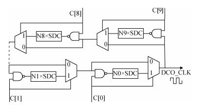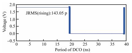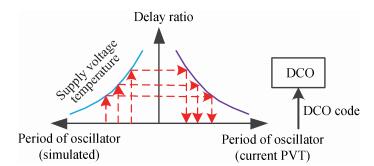
Fig. 1.
The basic theory of clock generator based on relative reference modeling.
SEMICONDUCTOR INTEGRATED CIRCUITS
Yapeng Sun1, Huidong Zhao2, Shushan Qiao2, , Yong Hei2 and Fuhai Zhang1
Corresponding author: Shushan Qiao, E-mail:qiaoshushan@ime.ac.cn
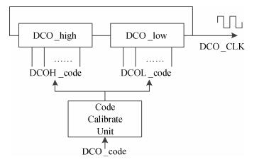
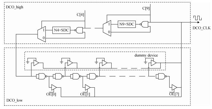
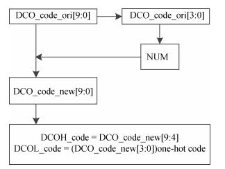
Abstract: In this paper, a novel hybrid digital-controlled oscillator (DCO) is proposed, which is used to improve the accuracy of the all-digital clock generator without reference source. The DCO with hybrid architecture consists of two parts: DCO_high and DCO_low. The DCO_high decides the coarse output frequency of DCO, and adopts the cascade structure to decrease the area. The DCO_low adopts the chain structure with three-state buffer, and decides the fine output frequency of DCO. Compared with traditional cascade DCO, the proposed hybrid DCO features higher precision with less inherent delay. Therefore the clock generator can tolerate process, voltage and temperature (PVT) variation and meet the needs of different conditions. The DCO is designed in SMIC 180 nm CMOS process with 0.021 mm2 chip area. The output frequency is adjusted from 15-120 MHz. The frequency error is less than 0.83% at 25 MHz with 1.6-1.8 V supply voltage and 0-80 ℃ temperature variations in TT, FF, SS corners.
Keywords: high accuracy DCO, all-digital, PVT variations
| [1] |
Kim C, Hwang I C, Kang S M. A low-power small-area ± 7.28-ps-jitter 1-GHz DLL-based clock generator. IEEE J Solid-State Circuits, 2002, 37(11): 1414 doi: 10.1109/JSSC.2002.803936
|
| [2] |
Lee J, Kim K, Lee J, et al. A 480-MHz to 1-GHz sub-picosecond clock generator with a fast and accurate automatic frequency calibration in 0.13-μm CMOS. IEEE Asian Solid-State Circuits Conference, 2007: 67 doi: 10.1155/2013/754206
|
| [3] |
Kumar M, Arya S K, Pandey S. Digitally controlled oscillator design with a variable capacitance XOR gate. J Semicond, 2011, 32(10): 105001 doi: 10.1088/1674-4926/32/10/105001
|
| [4] |
Xu W L, Wu D, Wei X M, et al. Low-noise sub-harmonic injection locked multiloop ring oscillator. J Semicond, 2016, 37(9): 095004 doi: 10.1088/1674-4926/37/9/095004
|
| [5] |
Zhang J C, Zhang Y M, Lv H L, et al. A Ku-band wide-tuning-range high-output-power VCO in InGaP/GaAs HBT technology. J Semicond, 2015, 36(6): 065010 doi: 10.1088/1674-4926/36/6/065010
|
| [6] |
Peng B H, Luo W, Zhao J C, et al. Frequency stability of an RF oscillator with an MEMS-based encapsulated resonator. J Semicond, 2015, 36(7): 074010 doi: 10.1088/1674-4926/36/7/074010
|
| [7] |
Satoh Y, Kobayashi H, Miyaba T, et al. A 2.9 mW, ± 85 ppm accuracy reference clock generator based on RC oscillator with on-chip temperature calibration. 2014 Symposium on VLSI Circuits Digest of Technical Papers, 2014: 1 https://www.researchgate.net/publication/269292690_A_29mW_-_85ppm_accuracy_reference_clock_generator_based_on_RC_oscillator_with_on-chip_temperature_calibration
|
| [8] |
Abbasizadeh H, Rikan B S, Lee K Y. A fully on-chip 25 MHz PVT-compensation CMOS Relaxation Oscillator. 2015 IFIP/IEEE International Conference on Very Large Scale Integration, 2015: 241 http://ieeexplore.ieee.org/abstract/document/7314423
|
| [9] |
Lee T J, Shmilovitz D, Hsieh Y J, et al. Temperature and process compensated clock generator using feedback TPC bias. 2012 IEEE International Conference on IC Design & Technology (ICICDT), 2012: 1 https://www.researchgate.net/publication/254043560_Temperature_and_process_compensated_clock_generator_using_feedback_TPC_bias
|
| [10] |
Wang Y, Chai K T C, Mu X, et al. A 1.5 ± 0.39 ppm/℃ temperature-compensated LC oscillator using constant-biased varactors. Microwave & Wireless Components Letters IEEE, 2015, 25(2): 130 http://ieeexplore.ieee.org/xpl/articleDetails.jsp?reload=true&arnumber=7004084&filter%3DAND%28p_IS_Number%3A7038238%29
|
| [11] |
Tian H H, Li Z Q, Chen P F, et al. A low-power and low-phase-noise LC digitally controlled oscillator featuring a novel capacitor bank. J Semicond, 2010, 31(12): 125003 doi: 10.1088/1674-4926/31/12/125003
|
| [12] |
Rout P K, Acharya D P, Panda G. A multiobjective optimization based fast and robust design methodology for low power and low phase noise current starved VCO. IEEE Trans Semicond Manufact, 2014, 27(1): 43 doi: 10.1109/TSM.2013.2295423
|
| [13] |
Maymandi-Nejad M, Sachdev M. A monotonic digitally controlled delay element. IEEE J Solid-State Circuits, 2005, 40(11): 2212 doi: 10.1109/JSSC.2005.857370
|
| [14] |
Yu C Y, Yu J Y, Lee C Y. A low voltage all-digital on-chip oscillator using relative reference modeling. IEEE Trans Very Large Scale Integra Syst, 2012, 20(9): 1615 doi: 10.1109/TVLSI.2011.2160301
|
| [15] |
Chung C C, Li J W. An all-digital on-chip silicon oscillator with automatic VT range selection relative modeling. 2013 IEEE International Symposium on Circuits and Systems (ISCAS), 2013: 2682 https://www.researchgate.net/publication/261192293_An_all-digital_on-chip_silicon_oscillator_with_automatic_VT_range_selection_relative_modeling
|
| [16] |
Wang C C, Wang D S, Sung T C, et al. A ± 3.07% frequency variation clock generator implemented using HV CMOS process. Microelectron J, 2015, 46(4): 285 doi: 10.1016/j.mejo.2014.12.008
|
| [17] |
Bako N, Baric A. A low-power, temperature and supply voltage compensated current starved ring oscillator. Microelectron J, 2013, 44(12): 1154 doi: 10.1016/j.mejo.2013.07.004
|
| [18] |
Tokunaga Y, Sakiyama S, Matsumoto A, et al. An on-chip CMOS relaxation oscillator with voltage averaging feedback. IEEE J Solid-State Circuits, 2010, 45(6): 1150 doi: 10.1109/JSSC.2010.2048732
|
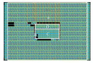
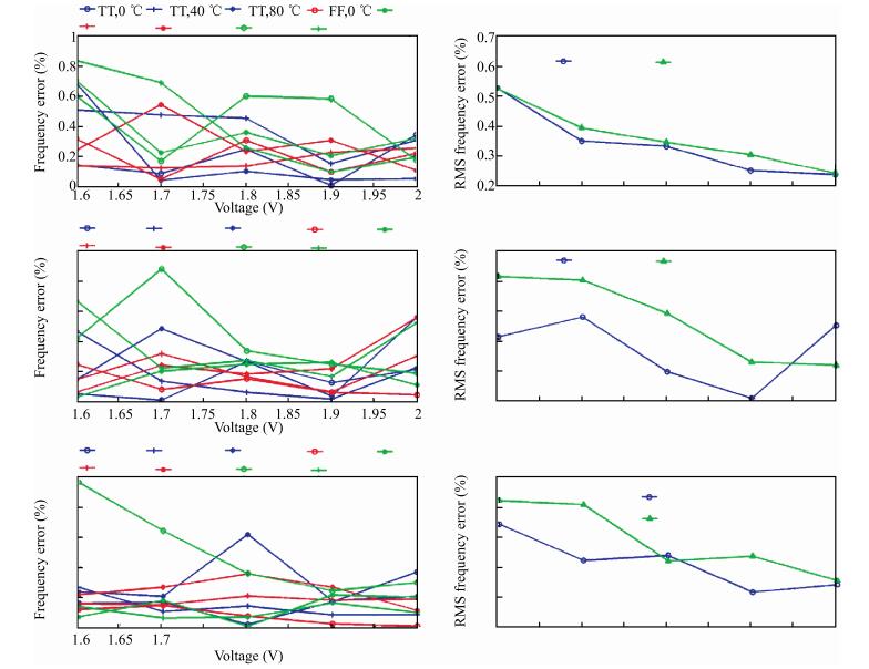
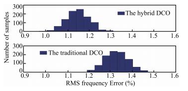
Table 1. Performance comparison.

|
| [1] |
Kim C, Hwang I C, Kang S M. A low-power small-area ± 7.28-ps-jitter 1-GHz DLL-based clock generator. IEEE J Solid-State Circuits, 2002, 37(11): 1414 doi: 10.1109/JSSC.2002.803936
|
| [2] |
Lee J, Kim K, Lee J, et al. A 480-MHz to 1-GHz sub-picosecond clock generator with a fast and accurate automatic frequency calibration in 0.13-μm CMOS. IEEE Asian Solid-State Circuits Conference, 2007: 67 doi: 10.1155/2013/754206
|
| [3] |
Kumar M, Arya S K, Pandey S. Digitally controlled oscillator design with a variable capacitance XOR gate. J Semicond, 2011, 32(10): 105001 doi: 10.1088/1674-4926/32/10/105001
|
| [4] |
Xu W L, Wu D, Wei X M, et al. Low-noise sub-harmonic injection locked multiloop ring oscillator. J Semicond, 2016, 37(9): 095004 doi: 10.1088/1674-4926/37/9/095004
|
| [5] |
Zhang J C, Zhang Y M, Lv H L, et al. A Ku-band wide-tuning-range high-output-power VCO in InGaP/GaAs HBT technology. J Semicond, 2015, 36(6): 065010 doi: 10.1088/1674-4926/36/6/065010
|
| [6] |
Peng B H, Luo W, Zhao J C, et al. Frequency stability of an RF oscillator with an MEMS-based encapsulated resonator. J Semicond, 2015, 36(7): 074010 doi: 10.1088/1674-4926/36/7/074010
|
| [7] |
Satoh Y, Kobayashi H, Miyaba T, et al. A 2.9 mW, ± 85 ppm accuracy reference clock generator based on RC oscillator with on-chip temperature calibration. 2014 Symposium on VLSI Circuits Digest of Technical Papers, 2014: 1 https://www.researchgate.net/publication/269292690_A_29mW_-_85ppm_accuracy_reference_clock_generator_based_on_RC_oscillator_with_on-chip_temperature_calibration
|
| [8] |
Abbasizadeh H, Rikan B S, Lee K Y. A fully on-chip 25 MHz PVT-compensation CMOS Relaxation Oscillator. 2015 IFIP/IEEE International Conference on Very Large Scale Integration, 2015: 241 http://ieeexplore.ieee.org/abstract/document/7314423
|
| [9] |
Lee T J, Shmilovitz D, Hsieh Y J, et al. Temperature and process compensated clock generator using feedback TPC bias. 2012 IEEE International Conference on IC Design & Technology (ICICDT), 2012: 1 https://www.researchgate.net/publication/254043560_Temperature_and_process_compensated_clock_generator_using_feedback_TPC_bias
|
| [10] |
Wang Y, Chai K T C, Mu X, et al. A 1.5 ± 0.39 ppm/℃ temperature-compensated LC oscillator using constant-biased varactors. Microwave & Wireless Components Letters IEEE, 2015, 25(2): 130 http://ieeexplore.ieee.org/xpl/articleDetails.jsp?reload=true&arnumber=7004084&filter%3DAND%28p_IS_Number%3A7038238%29
|
| [11] |
Tian H H, Li Z Q, Chen P F, et al. A low-power and low-phase-noise LC digitally controlled oscillator featuring a novel capacitor bank. J Semicond, 2010, 31(12): 125003 doi: 10.1088/1674-4926/31/12/125003
|
| [12] |
Rout P K, Acharya D P, Panda G. A multiobjective optimization based fast and robust design methodology for low power and low phase noise current starved VCO. IEEE Trans Semicond Manufact, 2014, 27(1): 43 doi: 10.1109/TSM.2013.2295423
|
| [13] |
Maymandi-Nejad M, Sachdev M. A monotonic digitally controlled delay element. IEEE J Solid-State Circuits, 2005, 40(11): 2212 doi: 10.1109/JSSC.2005.857370
|
| [14] |
Yu C Y, Yu J Y, Lee C Y. A low voltage all-digital on-chip oscillator using relative reference modeling. IEEE Trans Very Large Scale Integra Syst, 2012, 20(9): 1615 doi: 10.1109/TVLSI.2011.2160301
|
| [15] |
Chung C C, Li J W. An all-digital on-chip silicon oscillator with automatic VT range selection relative modeling. 2013 IEEE International Symposium on Circuits and Systems (ISCAS), 2013: 2682 https://www.researchgate.net/publication/261192293_An_all-digital_on-chip_silicon_oscillator_with_automatic_VT_range_selection_relative_modeling
|
| [16] |
Wang C C, Wang D S, Sung T C, et al. A ± 3.07% frequency variation clock generator implemented using HV CMOS process. Microelectron J, 2015, 46(4): 285 doi: 10.1016/j.mejo.2014.12.008
|
| [17] |
Bako N, Baric A. A low-power, temperature and supply voltage compensated current starved ring oscillator. Microelectron J, 2013, 44(12): 1154 doi: 10.1016/j.mejo.2013.07.004
|
| [18] |
Tokunaga Y, Sakiyama S, Matsumoto A, et al. An on-chip CMOS relaxation oscillator with voltage averaging feedback. IEEE J Solid-State Circuits, 2010, 45(6): 1150 doi: 10.1109/JSSC.2010.2048732
|


Article views: 3711 Times PDF downloads: 36 Times Cited by: 0 Times
Received: 09 August 2016 Revised: 15 January 2017 Online: Published: 01 July 2017
| Citation: |
Yapeng Sun, Huidong Zhao, Shushan Qiao, Yong Hei, Fuhai Zhang. A high-accuracy DCO with hybrid architecture[J]. Journal of Semiconductors, 2017, 38(7): 075004. doi: 10.1088/1674-4926/38/7/075004
****
Y P Sun, H D Zhao, S S Qiao, Y Hei, F H Zhang. A high-accuracy DCO with hybrid architecture[J]. J. Semicond., 2017, 38(7): 075004. doi: 10.1088/1674-4926/38/7/075004.

|
| [1] |
Kim C, Hwang I C, Kang S M. A low-power small-area ± 7.28-ps-jitter 1-GHz DLL-based clock generator. IEEE J Solid-State Circuits, 2002, 37(11): 1414 doi: 10.1109/JSSC.2002.803936
|
| [2] |
Lee J, Kim K, Lee J, et al. A 480-MHz to 1-GHz sub-picosecond clock generator with a fast and accurate automatic frequency calibration in 0.13-μm CMOS. IEEE Asian Solid-State Circuits Conference, 2007: 67 doi: 10.1155/2013/754206
|
| [3] |
Kumar M, Arya S K, Pandey S. Digitally controlled oscillator design with a variable capacitance XOR gate. J Semicond, 2011, 32(10): 105001 doi: 10.1088/1674-4926/32/10/105001
|
| [4] |
Xu W L, Wu D, Wei X M, et al. Low-noise sub-harmonic injection locked multiloop ring oscillator. J Semicond, 2016, 37(9): 095004 doi: 10.1088/1674-4926/37/9/095004
|
| [5] |
Zhang J C, Zhang Y M, Lv H L, et al. A Ku-band wide-tuning-range high-output-power VCO in InGaP/GaAs HBT technology. J Semicond, 2015, 36(6): 065010 doi: 10.1088/1674-4926/36/6/065010
|
| [6] |
Peng B H, Luo W, Zhao J C, et al. Frequency stability of an RF oscillator with an MEMS-based encapsulated resonator. J Semicond, 2015, 36(7): 074010 doi: 10.1088/1674-4926/36/7/074010
|
| [7] |
Satoh Y, Kobayashi H, Miyaba T, et al. A 2.9 mW, ± 85 ppm accuracy reference clock generator based on RC oscillator with on-chip temperature calibration. 2014 Symposium on VLSI Circuits Digest of Technical Papers, 2014: 1 https://www.researchgate.net/publication/269292690_A_29mW_-_85ppm_accuracy_reference_clock_generator_based_on_RC_oscillator_with_on-chip_temperature_calibration
|
| [8] |
Abbasizadeh H, Rikan B S, Lee K Y. A fully on-chip 25 MHz PVT-compensation CMOS Relaxation Oscillator. 2015 IFIP/IEEE International Conference on Very Large Scale Integration, 2015: 241 http://ieeexplore.ieee.org/abstract/document/7314423
|
| [9] |
Lee T J, Shmilovitz D, Hsieh Y J, et al. Temperature and process compensated clock generator using feedback TPC bias. 2012 IEEE International Conference on IC Design & Technology (ICICDT), 2012: 1 https://www.researchgate.net/publication/254043560_Temperature_and_process_compensated_clock_generator_using_feedback_TPC_bias
|
| [10] |
Wang Y, Chai K T C, Mu X, et al. A 1.5 ± 0.39 ppm/℃ temperature-compensated LC oscillator using constant-biased varactors. Microwave & Wireless Components Letters IEEE, 2015, 25(2): 130 http://ieeexplore.ieee.org/xpl/articleDetails.jsp?reload=true&arnumber=7004084&filter%3DAND%28p_IS_Number%3A7038238%29
|
| [11] |
Tian H H, Li Z Q, Chen P F, et al. A low-power and low-phase-noise LC digitally controlled oscillator featuring a novel capacitor bank. J Semicond, 2010, 31(12): 125003 doi: 10.1088/1674-4926/31/12/125003
|
| [12] |
Rout P K, Acharya D P, Panda G. A multiobjective optimization based fast and robust design methodology for low power and low phase noise current starved VCO. IEEE Trans Semicond Manufact, 2014, 27(1): 43 doi: 10.1109/TSM.2013.2295423
|
| [13] |
Maymandi-Nejad M, Sachdev M. A monotonic digitally controlled delay element. IEEE J Solid-State Circuits, 2005, 40(11): 2212 doi: 10.1109/JSSC.2005.857370
|
| [14] |
Yu C Y, Yu J Y, Lee C Y. A low voltage all-digital on-chip oscillator using relative reference modeling. IEEE Trans Very Large Scale Integra Syst, 2012, 20(9): 1615 doi: 10.1109/TVLSI.2011.2160301
|
| [15] |
Chung C C, Li J W. An all-digital on-chip silicon oscillator with automatic VT range selection relative modeling. 2013 IEEE International Symposium on Circuits and Systems (ISCAS), 2013: 2682 https://www.researchgate.net/publication/261192293_An_all-digital_on-chip_silicon_oscillator_with_automatic_VT_range_selection_relative_modeling
|
| [16] |
Wang C C, Wang D S, Sung T C, et al. A ± 3.07% frequency variation clock generator implemented using HV CMOS process. Microelectron J, 2015, 46(4): 285 doi: 10.1016/j.mejo.2014.12.008
|
| [17] |
Bako N, Baric A. A low-power, temperature and supply voltage compensated current starved ring oscillator. Microelectron J, 2013, 44(12): 1154 doi: 10.1016/j.mejo.2013.07.004
|
| [18] |
Tokunaga Y, Sakiyama S, Matsumoto A, et al. An on-chip CMOS relaxation oscillator with voltage averaging feedback. IEEE J Solid-State Circuits, 2010, 45(6): 1150 doi: 10.1109/JSSC.2010.2048732
|

 WeChat ID
Journal of Semiconductors © 2017 All Rights Reserved 京ICP备05085259号-2

 DownLoad: