Fig. 1.
The parallel-plate electrodes that generate electrostatic force.
SEMICONDUCTOR DEVICES
Nan Liu1, 2, Yan Su1, 2, Xin Tong1, 2, Guowei Han1, , Chaowei Si1, Zhaofeng Li1, 3, and Jin Ning1, 4, 5
Corresponding author: Guowei Han, Email: hangw1984@semi.ac.cn; Zhaofeng Li, lizhaofeng@semi.ac.cn
Abstract: Output voltage drifting was observed in MEMS gyroscopes. Other than the quadrature error, frequency mismatch and quality factor, the dielectric parasitic charge was thought to be a major determinant. We studied the mechanism and variation of the parasitic charge in the MEMS gyroscopes, and analyzed the effect of the parasitic charge on the output stability. This phenomenon was extremely obvious in the Pyrex encapsulated MEMS gyroscopes. Due to the DC voltage required for the electrostatic actuation, the parasitic charge in the dielectric layer would accumulate and induce a residual voltage. This voltage had an impact on the resonant frequency of the gyroscopes, so as to affect the output stability. The theoretical studies were also confirmed by our experimental results. It was shown that the parasitic charge was harmful to the output stability of MEMS gyroscopes.
Keywords: dielectric parasitic charge, micro-electro-mechanical system (MEMS) gyroscopes, frequency drift, DC voltage
| [1] |
Nakamura S. MEMS inertial sensor toward higher accuracy & multi-axis sensing. Proceedings of the IEEE Conference on Sensors, 2005: 939
|
| [2] |
Zhong W W, Han G W, Si C W, et al. Fabrication and characterization of an SOI MEMS gyroscope. J Semicond, 2013, 34(6): 064004 doi: 10.1088/1674-4926/34/6/064004
|
| [3] |
Xia D Z, Sheng X, Wang S R. A digital prototype miniature silicon microgyroscope. IEEE International Conference on Nano/micro Engineered and Molecular Systems IEEE, 2010: 429
|
| [4] |
Acar C, Shkel A. MEMS vibratory gyroscopes structural approaches to improve robustness. Springer Science Business Media, LLC, 2009
|
| [5] |
Henry J A, Wang Y, Sengupta D, et al. Understanding the effects of surface chemistry on Q: mechanical energy dissipation in alkyl-terminated (C-1-C-18) micromechanical silicon resonators. J Phys Chem B, 2007, 111(1): 88 doi: 10.1021/jp0654011
|
| [6] |
Li S S, Lin Y W, Xie Y, et al. Charge-biased vibrating micromechanical resonators. IEEE Ultrasonics Symposium, 2005: 1596
|
| [7] |
Bienstman J, Tilmans H A C, Peeters E J E A, et al. An oscillator circuit for electrostatically driven silicon-based one-port resonators. Sens Actuators A, 1996, 52(1-3): 179 doi: 10.1016/0924-4247(96)80146-4
|
| [8] |
Zhou W, He J B, He X P, et al. Dielectric charging induced drift in micro device reliability – a review. Microelectron Reliab, 2016, 66(2016): 1
|
| [9] |
Qu H, Yu H J, Zhou W, et al. Effects of dielectric charging on the output voltage of a capacitive accelerometer. J Micromechan Microeng, 2016, 26(11): 115001 doi: 10.1088/0960-1317/26/11/115001
|
| [10] |
Ward P. Split electrode to minimize charge transients, motor amplitude mismatch errors, and sensitivity to vertical translation in tuning fork gyros and other devices. USA Patent, US5911156, 1999
|
| [11] |
Wang X L. Research and experiment on closed-loop detection and quadrature error correction technology of silicon micro-gyroscope. PhD Dissertation, Southeast University, 2014 (in Chinese)
|
| [12] |
Seshia A A, Palaniapan M, Roessig T A, et al. A vacuum packaged surface micromachined resonant accelerometer. J Microelectromech Syst, 2002, 11(6): 784 doi: 10.1109/JMEMS.2002.805207
|
| [13] |
Lee B L, Oh C H, Lee S, et al. A vacuum packaged differential resonant accelerometer using gap sensitive electrostatic stiffness changing effect. Proc IEEE MEMS, 2000: 352
|
| [14] |
Tavassolian N. Dielectric charging in capacitive RF MEMS switches with silicon nitride and silicon dioxide. PhD Dissertation, Georgia Institute of Technology, 2011
|
| [15] |
Wibbeler J, Pfeifer G, Hietschold M. Parasitic charging of dielectric surfaces in capacitive microelectromechanical systems (MEMS). Sens Actuators A, 1998, 71(1-2): 74 doi: 10.1016/S0924-4247(98)00155-1
|
| [16] |
Li G, Zhan L, San H, et al. Influence of ion implantation on dielectric charging in capacitive RF MEMS switches. Proc SPIE, 2008, 6836: 68360J
|
| [17] |
Zhan L, San H, Li G, et al. Charge accumulation in composite dielectric layers in capacitive RF MEMS switches. Proc SPIE, 2007, 6836: 68360Z
|
| [18] |
Koutsoureli M, Michalas L, Papandreou E, et al. Induced charging phenomena on SiNx dielectric films used in RF MEMS capacitive switches. Microelectron Reliab, 2015, 55(9-10): 1911 doi: 10.1016/j.microrel.2015.06.007
|
| [19] |
Dorsey K. Dielectric charging in CMOS MEMS. PhD Dissertation, Carnegie Mellon University, 2013
|
| [20] |
Zaghloul U, Bhushan B, Pons P, et al. On the influence of environment gases, relative humidity and gas purification on dielectric charging/discharging processes in electrostatically driven MEMS/NEMS devices. Nanotechnology, 2010, 22: 035705
|
| [21] |
Koszewski A, Souchon F, Dieppedale C, et al. Physical model of dielectric charging in MEMS. J Micromech Microeng, 2013, 23(4): 783
|
| [22] |
Zhang J, Sun J Y, Zhang Z H, et al. Effects of dielectric charging on MEMS-based grating light modulator. Microsyst Technol, 2009, 15(5): 745 doi: 10.1007/s00542-009-0784-7
|
| [23] |
Jan M T, Ahmada F, Hamid N H B, et al. Experimental investigation of temperature and relative humidity effects on resonance frequency and quality factor of CMOS-MEMS paddle resonator. Microelectron Reliab, 2016, 63(1): 82
|
| [24] |
Giessibl F, Sugawara Y, Morita S, et al. Noncontact atomic force microscopy and related topics. Nanotribology Nanomechanics, Berlin, Springer, 2005
|
| [25] |
Blokhina E, Gorreta S, Lopez D, et al. Dielectric charge control in electrostatic MEMS positioners varactors. J Microelectromech Syst, 2012, 21(3): 559 doi: 10.1109/JMEMS.2011.2182500
|
| [26] |
Hedenstierna N, Habibi S, Nilsen S M, et al. Bulk micromachined angular rate sensor based on the ‘butterfly’-gyro structure. MEMS, 2001: 178
|
| [27] |
Kalicinski S, Wevers M, DeWolf I. Charging and discharging phenomena in electrostatically-driven single-crystal-silicon MEM resonators: DC bias dependence and influence on the series resonance frequency. Microelectron Reliab, 2008, 48(8-9): 1221 doi: 10.1016/j.microrel.2008.07.024
|
| [28] |
Daigler R, Papandreou E, Koutsoureli M, et al. Effect of deposition conditions on charging processes in SiNx: Application to RF-MEMS capacitive switches. Microelectron Eng, 2009, 86(3): 404 doi: 10.1016/j.mee.2008.12.014
|
| [29] |
Lamhamdi M, Guastavino J, Boudou L, et al. Charging-effects in RF capacitive switches influence of insulating layers composition. Microelectron Reliab, 2006, 46(9-11): 1700 doi: 10.1016/j.microrel.2006.07.046
|
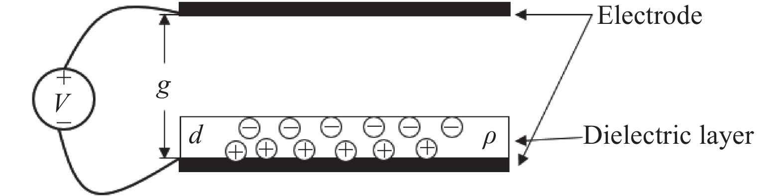
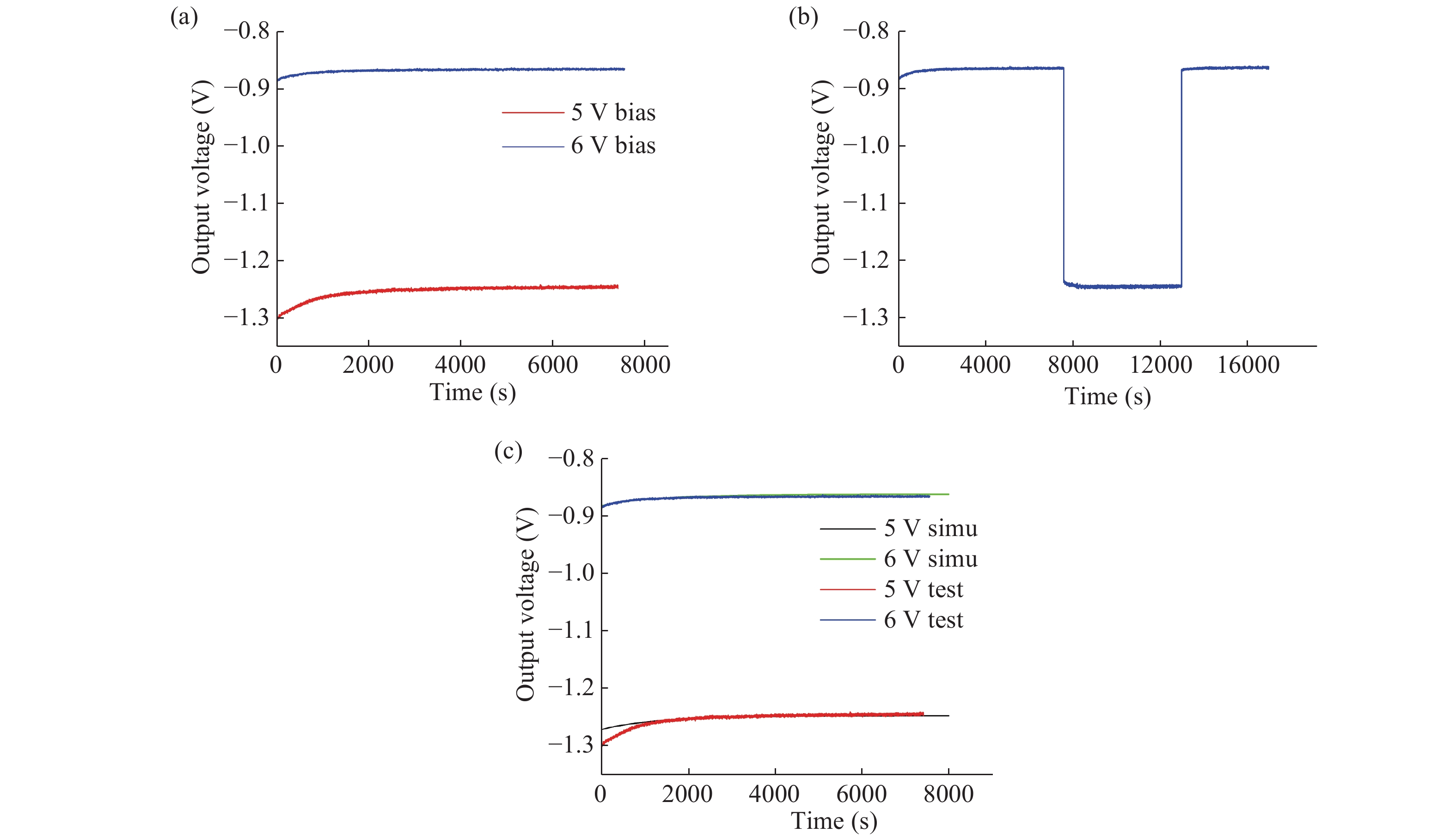
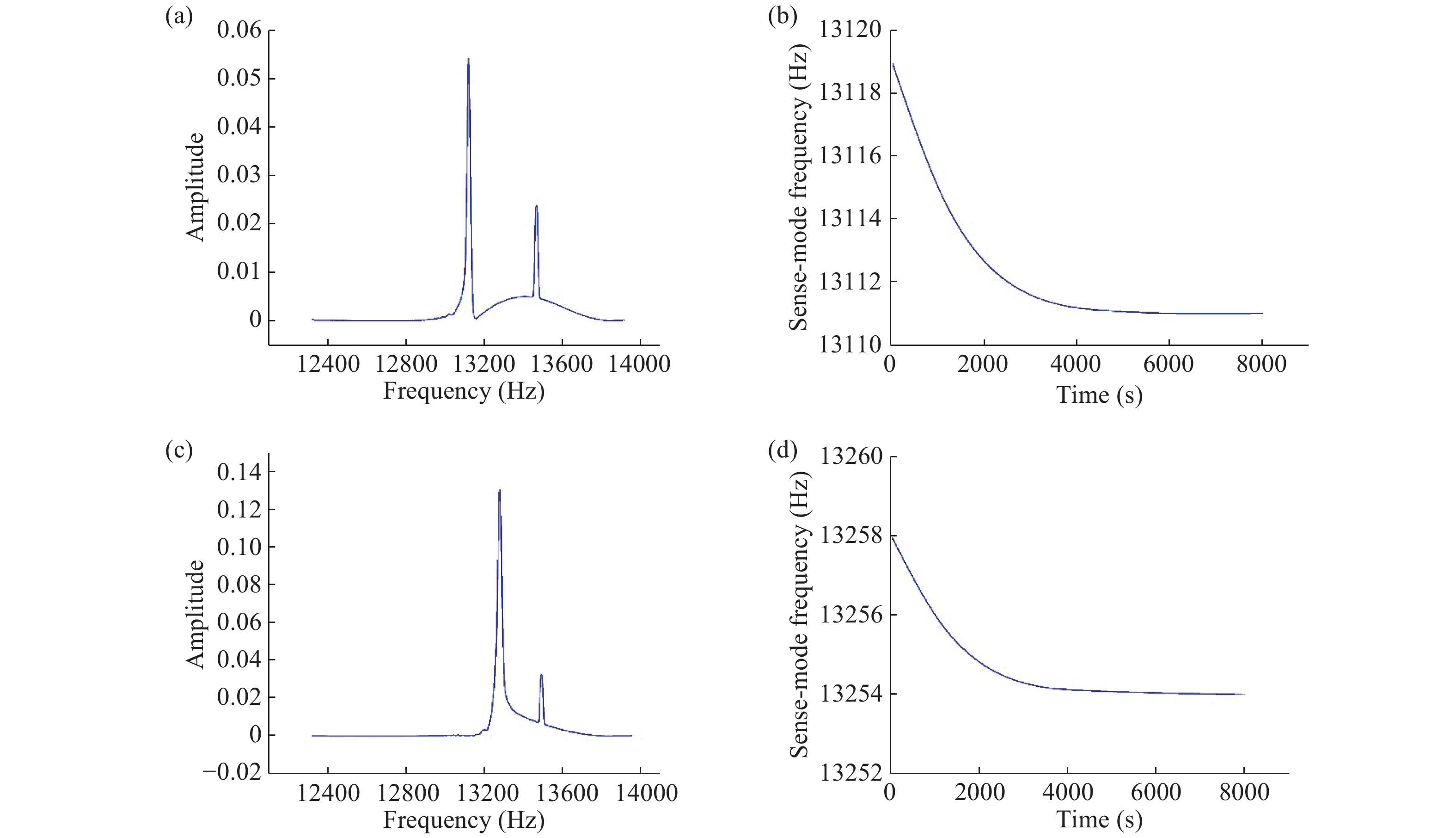

Table 1. The parameters of the gyroscope and some constants used in simulation.
| Parameter | Symbol | Value | Unit |
| Drive-mode frequency | wx | 13.467 | kHz |
| Drive-mode stiffness | kx | 50 000 | N/m |
| Sense-mode stiffness | ky | 870 | N/m |
| Sense-mode mass | my | 1.2 × 10⁻⁷ | kg |
| Gap | g | 2 × 10⁻⁶ | m |
| Area | A | 1.4 × 10⁻⁶ | m2 |
| Air permittivity | ε0 | 8.854 × 10⁻¹² | N/m |
| Relative permittivity | εr | 3.9 | − |
| Gain constant (6 V) | G | 3.2 × 10⁸ | V·kHz2 |
| Gain constant (5 V) | G | 2.8 × 10⁸ | V·kHz2 |
 DownLoad: CSV
| [1] |
Nakamura S. MEMS inertial sensor toward higher accuracy & multi-axis sensing. Proceedings of the IEEE Conference on Sensors, 2005: 939
|
| [2] |
Zhong W W, Han G W, Si C W, et al. Fabrication and characterization of an SOI MEMS gyroscope. J Semicond, 2013, 34(6): 064004 doi: 10.1088/1674-4926/34/6/064004
|
| [3] |
Xia D Z, Sheng X, Wang S R. A digital prototype miniature silicon microgyroscope. IEEE International Conference on Nano/micro Engineered and Molecular Systems IEEE, 2010: 429
|
| [4] |
Acar C, Shkel A. MEMS vibratory gyroscopes structural approaches to improve robustness. Springer Science Business Media, LLC, 2009
|
| [5] |
Henry J A, Wang Y, Sengupta D, et al. Understanding the effects of surface chemistry on Q: mechanical energy dissipation in alkyl-terminated (C-1-C-18) micromechanical silicon resonators. J Phys Chem B, 2007, 111(1): 88 doi: 10.1021/jp0654011
|
| [6] |
Li S S, Lin Y W, Xie Y, et al. Charge-biased vibrating micromechanical resonators. IEEE Ultrasonics Symposium, 2005: 1596
|
| [7] |
Bienstman J, Tilmans H A C, Peeters E J E A, et al. An oscillator circuit for electrostatically driven silicon-based one-port resonators. Sens Actuators A, 1996, 52(1-3): 179 doi: 10.1016/0924-4247(96)80146-4
|
| [8] |
Zhou W, He J B, He X P, et al. Dielectric charging induced drift in micro device reliability – a review. Microelectron Reliab, 2016, 66(2016): 1
|
| [9] |
Qu H, Yu H J, Zhou W, et al. Effects of dielectric charging on the output voltage of a capacitive accelerometer. J Micromechan Microeng, 2016, 26(11): 115001 doi: 10.1088/0960-1317/26/11/115001
|
| [10] |
Ward P. Split electrode to minimize charge transients, motor amplitude mismatch errors, and sensitivity to vertical translation in tuning fork gyros and other devices. USA Patent, US5911156, 1999
|
| [11] |
Wang X L. Research and experiment on closed-loop detection and quadrature error correction technology of silicon micro-gyroscope. PhD Dissertation, Southeast University, 2014 (in Chinese)
|
| [12] |
Seshia A A, Palaniapan M, Roessig T A, et al. A vacuum packaged surface micromachined resonant accelerometer. J Microelectromech Syst, 2002, 11(6): 784 doi: 10.1109/JMEMS.2002.805207
|
| [13] |
Lee B L, Oh C H, Lee S, et al. A vacuum packaged differential resonant accelerometer using gap sensitive electrostatic stiffness changing effect. Proc IEEE MEMS, 2000: 352
|
| [14] |
Tavassolian N. Dielectric charging in capacitive RF MEMS switches with silicon nitride and silicon dioxide. PhD Dissertation, Georgia Institute of Technology, 2011
|
| [15] |
Wibbeler J, Pfeifer G, Hietschold M. Parasitic charging of dielectric surfaces in capacitive microelectromechanical systems (MEMS). Sens Actuators A, 1998, 71(1-2): 74 doi: 10.1016/S0924-4247(98)00155-1
|
| [16] |
Li G, Zhan L, San H, et al. Influence of ion implantation on dielectric charging in capacitive RF MEMS switches. Proc SPIE, 2008, 6836: 68360J
|
| [17] |
Zhan L, San H, Li G, et al. Charge accumulation in composite dielectric layers in capacitive RF MEMS switches. Proc SPIE, 2007, 6836: 68360Z
|
| [18] |
Koutsoureli M, Michalas L, Papandreou E, et al. Induced charging phenomena on SiNx dielectric films used in RF MEMS capacitive switches. Microelectron Reliab, 2015, 55(9-10): 1911 doi: 10.1016/j.microrel.2015.06.007
|
| [19] |
Dorsey K. Dielectric charging in CMOS MEMS. PhD Dissertation, Carnegie Mellon University, 2013
|
| [20] |
Zaghloul U, Bhushan B, Pons P, et al. On the influence of environment gases, relative humidity and gas purification on dielectric charging/discharging processes in electrostatically driven MEMS/NEMS devices. Nanotechnology, 2010, 22: 035705
|
| [21] |
Koszewski A, Souchon F, Dieppedale C, et al. Physical model of dielectric charging in MEMS. J Micromech Microeng, 2013, 23(4): 783
|
| [22] |
Zhang J, Sun J Y, Zhang Z H, et al. Effects of dielectric charging on MEMS-based grating light modulator. Microsyst Technol, 2009, 15(5): 745 doi: 10.1007/s00542-009-0784-7
|
| [23] |
Jan M T, Ahmada F, Hamid N H B, et al. Experimental investigation of temperature and relative humidity effects on resonance frequency and quality factor of CMOS-MEMS paddle resonator. Microelectron Reliab, 2016, 63(1): 82
|
| [24] |
Giessibl F, Sugawara Y, Morita S, et al. Noncontact atomic force microscopy and related topics. Nanotribology Nanomechanics, Berlin, Springer, 2005
|
| [25] |
Blokhina E, Gorreta S, Lopez D, et al. Dielectric charge control in electrostatic MEMS positioners varactors. J Microelectromech Syst, 2012, 21(3): 559 doi: 10.1109/JMEMS.2011.2182500
|
| [26] |
Hedenstierna N, Habibi S, Nilsen S M, et al. Bulk micromachined angular rate sensor based on the ‘butterfly’-gyro structure. MEMS, 2001: 178
|
| [27] |
Kalicinski S, Wevers M, DeWolf I. Charging and discharging phenomena in electrostatically-driven single-crystal-silicon MEM resonators: DC bias dependence and influence on the series resonance frequency. Microelectron Reliab, 2008, 48(8-9): 1221 doi: 10.1016/j.microrel.2008.07.024
|
| [28] |
Daigler R, Papandreou E, Koutsoureli M, et al. Effect of deposition conditions on charging processes in SiNx: Application to RF-MEMS capacitive switches. Microelectron Eng, 2009, 86(3): 404 doi: 10.1016/j.mee.2008.12.014
|
| [29] |
Lamhamdi M, Guastavino J, Boudou L, et al. Charging-effects in RF capacitive switches influence of insulating layers composition. Microelectron Reliab, 2006, 46(9-11): 1700 doi: 10.1016/j.microrel.2006.07.046
|


Article views: 4651 Times PDF downloads: 109 Times Cited by: 0 Times
Received: 09 December 2017 Revised: 06 February 2018 Online: Accepted Manuscript: 04 April 2018Uncorrected proof: 12 April 2018Published: 09 August 2018
| Citation: |
Nan Liu, Yan Su, Xin Tong, Guowei Han, Chaowei Si, Zhaofeng Li, Jin Ning. The effect of parasitic charge on the output stability of MEMS gyroscopes[J]. Journal of Semiconductors, 2018, 39(8): 084002. doi: 10.1088/1674-4926/39/8/084002
****
N Liu, Y Su, X Tong, G W Han, C W Si, Z F Li, J Ning, The effect of parasitic charge on the output stability of MEMS gyroscopes[J]. J. Semicond., 2018, 39(8): 084002. doi: 10.1088/1674-4926/39/8/084002.

|
| [1] |
Nakamura S. MEMS inertial sensor toward higher accuracy & multi-axis sensing. Proceedings of the IEEE Conference on Sensors, 2005: 939
|
| [2] |
Zhong W W, Han G W, Si C W, et al. Fabrication and characterization of an SOI MEMS gyroscope. J Semicond, 2013, 34(6): 064004 doi: 10.1088/1674-4926/34/6/064004
|
| [3] |
Xia D Z, Sheng X, Wang S R. A digital prototype miniature silicon microgyroscope. IEEE International Conference on Nano/micro Engineered and Molecular Systems IEEE, 2010: 429
|
| [4] |
Acar C, Shkel A. MEMS vibratory gyroscopes structural approaches to improve robustness. Springer Science Business Media, LLC, 2009
|
| [5] |
Henry J A, Wang Y, Sengupta D, et al. Understanding the effects of surface chemistry on Q: mechanical energy dissipation in alkyl-terminated (C-1-C-18) micromechanical silicon resonators. J Phys Chem B, 2007, 111(1): 88 doi: 10.1021/jp0654011
|
| [6] |
Li S S, Lin Y W, Xie Y, et al. Charge-biased vibrating micromechanical resonators. IEEE Ultrasonics Symposium, 2005: 1596
|
| [7] |
Bienstman J, Tilmans H A C, Peeters E J E A, et al. An oscillator circuit for electrostatically driven silicon-based one-port resonators. Sens Actuators A, 1996, 52(1-3): 179 doi: 10.1016/0924-4247(96)80146-4
|
| [8] |
Zhou W, He J B, He X P, et al. Dielectric charging induced drift in micro device reliability – a review. Microelectron Reliab, 2016, 66(2016): 1
|
| [9] |
Qu H, Yu H J, Zhou W, et al. Effects of dielectric charging on the output voltage of a capacitive accelerometer. J Micromechan Microeng, 2016, 26(11): 115001 doi: 10.1088/0960-1317/26/11/115001
|
| [10] |
Ward P. Split electrode to minimize charge transients, motor amplitude mismatch errors, and sensitivity to vertical translation in tuning fork gyros and other devices. USA Patent, US5911156, 1999
|
| [11] |
Wang X L. Research and experiment on closed-loop detection and quadrature error correction technology of silicon micro-gyroscope. PhD Dissertation, Southeast University, 2014 (in Chinese)
|
| [12] |
Seshia A A, Palaniapan M, Roessig T A, et al. A vacuum packaged surface micromachined resonant accelerometer. J Microelectromech Syst, 2002, 11(6): 784 doi: 10.1109/JMEMS.2002.805207
|
| [13] |
Lee B L, Oh C H, Lee S, et al. A vacuum packaged differential resonant accelerometer using gap sensitive electrostatic stiffness changing effect. Proc IEEE MEMS, 2000: 352
|
| [14] |
Tavassolian N. Dielectric charging in capacitive RF MEMS switches with silicon nitride and silicon dioxide. PhD Dissertation, Georgia Institute of Technology, 2011
|
| [15] |
Wibbeler J, Pfeifer G, Hietschold M. Parasitic charging of dielectric surfaces in capacitive microelectromechanical systems (MEMS). Sens Actuators A, 1998, 71(1-2): 74 doi: 10.1016/S0924-4247(98)00155-1
|
| [16] |
Li G, Zhan L, San H, et al. Influence of ion implantation on dielectric charging in capacitive RF MEMS switches. Proc SPIE, 2008, 6836: 68360J
|
| [17] |
Zhan L, San H, Li G, et al. Charge accumulation in composite dielectric layers in capacitive RF MEMS switches. Proc SPIE, 2007, 6836: 68360Z
|
| [18] |
Koutsoureli M, Michalas L, Papandreou E, et al. Induced charging phenomena on SiNx dielectric films used in RF MEMS capacitive switches. Microelectron Reliab, 2015, 55(9-10): 1911 doi: 10.1016/j.microrel.2015.06.007
|
| [19] |
Dorsey K. Dielectric charging in CMOS MEMS. PhD Dissertation, Carnegie Mellon University, 2013
|
| [20] |
Zaghloul U, Bhushan B, Pons P, et al. On the influence of environment gases, relative humidity and gas purification on dielectric charging/discharging processes in electrostatically driven MEMS/NEMS devices. Nanotechnology, 2010, 22: 035705
|
| [21] |
Koszewski A, Souchon F, Dieppedale C, et al. Physical model of dielectric charging in MEMS. J Micromech Microeng, 2013, 23(4): 783
|
| [22] |
Zhang J, Sun J Y, Zhang Z H, et al. Effects of dielectric charging on MEMS-based grating light modulator. Microsyst Technol, 2009, 15(5): 745 doi: 10.1007/s00542-009-0784-7
|
| [23] |
Jan M T, Ahmada F, Hamid N H B, et al. Experimental investigation of temperature and relative humidity effects on resonance frequency and quality factor of CMOS-MEMS paddle resonator. Microelectron Reliab, 2016, 63(1): 82
|
| [24] |
Giessibl F, Sugawara Y, Morita S, et al. Noncontact atomic force microscopy and related topics. Nanotribology Nanomechanics, Berlin, Springer, 2005
|
| [25] |
Blokhina E, Gorreta S, Lopez D, et al. Dielectric charge control in electrostatic MEMS positioners varactors. J Microelectromech Syst, 2012, 21(3): 559 doi: 10.1109/JMEMS.2011.2182500
|
| [26] |
Hedenstierna N, Habibi S, Nilsen S M, et al. Bulk micromachined angular rate sensor based on the ‘butterfly’-gyro structure. MEMS, 2001: 178
|
| [27] |
Kalicinski S, Wevers M, DeWolf I. Charging and discharging phenomena in electrostatically-driven single-crystal-silicon MEM resonators: DC bias dependence and influence on the series resonance frequency. Microelectron Reliab, 2008, 48(8-9): 1221 doi: 10.1016/j.microrel.2008.07.024
|
| [28] |
Daigler R, Papandreou E, Koutsoureli M, et al. Effect of deposition conditions on charging processes in SiNx: Application to RF-MEMS capacitive switches. Microelectron Eng, 2009, 86(3): 404 doi: 10.1016/j.mee.2008.12.014
|
| [29] |
Lamhamdi M, Guastavino J, Boudou L, et al. Charging-effects in RF capacitive switches influence of insulating layers composition. Microelectron Reliab, 2006, 46(9-11): 1700 doi: 10.1016/j.microrel.2006.07.046
|

 WeChat ID
Journal of Semiconductors © 2017 All Rights Reserved 京ICP备05085259号-2