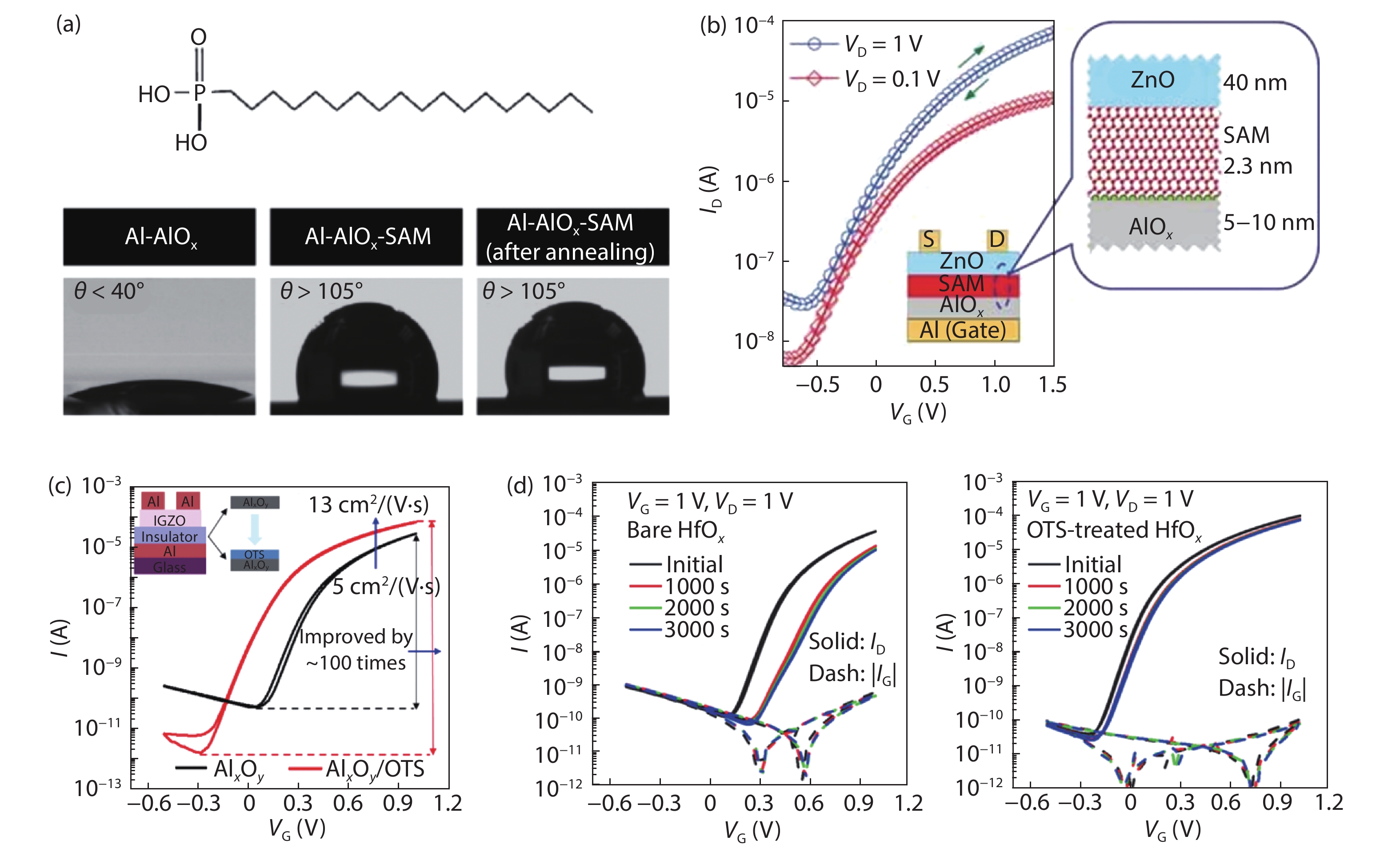
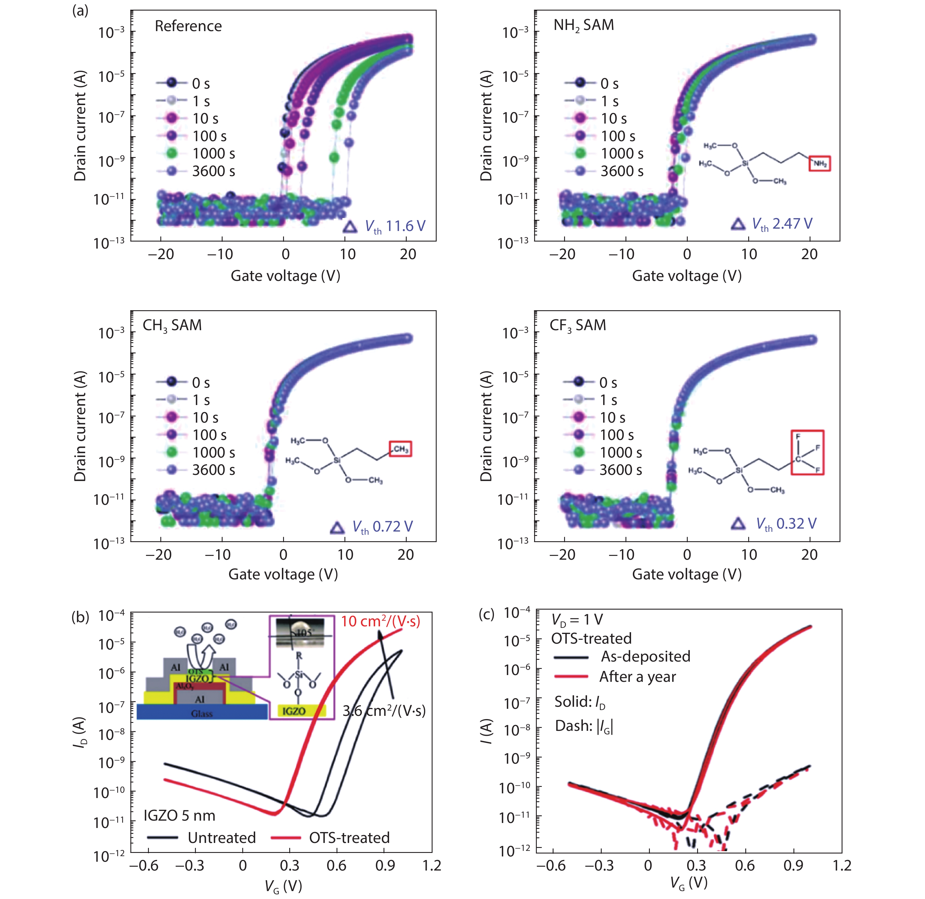
J. Semicond. > 2021, Volume 42 > Issue 3 > 030203

RESEARCH HIGHLIGHTS

Self-assembled monolayers enhance the performance of oxide thin-film transistors

Wensi Cai1, Zhigang Zang1, and Liming Ding2,

+ Author Affiliations

 Corresponding author: Zhigang Zang, zangzg@cqu.edu.cn; Liming Ding, ding@nanoctr.cn

DOI: 10.1088/1674-4926/42/3/030203

PDF

Turn off MathJax

Thin-film transistors (TFTs) based on oxide semiconductors have gained a lot of attention in applications such as displays and sensors particularly in recent years due to the advantages of oxide semiconductors like high mobility, good uniformity over large area and low deposition temperature[1-4]. However, the defects/traps at dielectric/channel interface and top surface of oxide TFTs might dramatically degrade device performance including current on/off ratio, mobility and most importantly stability[5, 6], making it quite urgent to systematically make effective interface engineering to improve TFT performance.

Traps on the top channel surface are mainly caused by the adsorbed water and oxygen molecules from air[7], which could be reduced by applying a passivation layer. One effective passivation layer is organic self-assembled monolayer (SAM), which can be formed densely on the surface of oxide semiconductors through the reaction with –OH groups, ensuring a reliable interface coupling between SAM and the channel layer and hence a good chemical stability[5, 8]. Compared with conventional inorganic passivation layers, SAMs can be easily applied on the top channel surface via vapor- or solution-based methods[8-10], which are plasma-free processes and can avoid the potential plasma damage to oxide semiconductors.

SAMs with different functional groups might give very different surface energy and dramatically affect the resulting device performance, especially the stability and hysteresis. Recently, Kim et al. investigated InGaZnO (IGZO) TFTs treated by SAMs with CH3, NH2 and CF3 functional groups, namely trimethoxy(propyl)silane (TPS), (3-aminopropyl)trimethoxysilane (APTMS), and trimethoxy(3,3,3-trifluoropropyl)silane (TFP) SAMs, respectively, as shown in the insets of Fig. 1(a)[11]. The untreated IGZO film shows a contact angle of 22.5°, after the treatment, it changes to 55.2° ± 1.7°, 81.9° ± 2.1° and 98.1° ± 2.3° for APTMS, TPS, and TFP treated IGZO films, respectively, suggesting a reduced surface energy. Such a reduced surface energy makes oxygen molecules being difficult to be adsorbed on the surface of the treated IGZO films. As a result, a decrease of both clockwise hysteresis and threshold voltage shift under the positive bias was observed after the treatment with a lowest value of 0.11 ± 0.06 V and 0.32 ± 0.26 V, respectively, achieved in TFP-treated IGZO TFTs (the lowest surface energy case), as shown in Fig. 1(a).

Figure  1.  (Color online) (a) Transfer characteristics of IGZO TFTs treated with different SAMs under positive bias stress. Insets show the chemical structures of SAM molecules. Reproduced with permission[11], Copyright 2021, IOP Publishing. (b) Transfer characteristics of IGZO TFTs with and without OTS treatment. (c) OTS-treated IGZO TFTs before and after being stored in air for a year. Reproduced with permission[8], Copyright 2021, American Chemical Society.

Alkyl chain lengths also affect device performance, as reported by Peng et al. who studied the relationship between SAM chain lengths and TFT performance by using triethoxysilane (TES) with three different alkyl chains, namely C1-TES, C8-TES and C18-TES[12]. All treated devices show an increased mobility and a decreased hysteresis compared with the untreated one. Among all treated devices, TFTs treated with C18-TES showed best performance with a mobility of 26.6 cm2/(V·s), which might be due to the formation of a well-ordered and more hydrophobic IGZO surface when treated with SAMs with longer alkyl chains. Similar effects were also reported by Chen et al. in InSnZnO TFTs treated with vapor-phase SAMs[9].

At smaller channel thicknesses, the accumulation layer approaches near the adsorbed water molecules on the top channel surface, inducing a strong carrier scattering and a more pronounced influence of top surface. To study whether the SAM treatment also works in TFTs with a thin channel layer, Song et al. made n-octadecyltrichlorosilane (OTS)-treated IGZO TFTs with different IGZO thicknesses[8]. As shown in Fig. 1(b), even at an IGZO thickness down to 5 nm, the treated devices show a high mobility of 10 cm2/(V·s) with a low subthreshold swing of 64 mV/dec and a high current on/off ratio larger than 106. Also, the device maintains a high performance even after being stored in air for a year (Fig. 1(c)), indicating that the top surface has been effectively passivated.

Besides being used as an effective passivation layer on the top surface of oxide TFTs, SAMs can also be applied at the dielectric/channel interface, which affects not only the dynamic performance but also the stability. SAM treatment is now a standard process in organic TFTs to reduce dielectric/channel interface traps and surface energy, but was seldom reported in oxide TFTs due to the potential damage to SAMs. By treating AlOx gate dielectrics with an n-octadecylphosphonic acid (ODPA), Bashir et al. reported high-performance ZnO TFTs made by spray pyrolyzing[13]. To study the survival of ODPA after the high-temperature ZnO deposition, they performed a contact angle measurement, and found that a high contact angle maintained even after a heat treatment of the sample at 400–450 °C in N2 (Fig. 2(a)), demonstrating the high stability of the ultra-thin SAM against heat. The SAM treatment here significantly reduces the gate leakage current, and as a result, the devices show a low operating voltage of 1.5 V with a current on/off ratio of 103 and a mobility of 8.3 cm2/(V·s) (Fig. 2(b)).

Figure  2.  (Color online) (a) Chemical structure of ODPA and contact angles of AlOx, SAM-treated AlOx before and after annealing. (b) Transfer characteristics of ZnO TFTs. Reproduced with permission[13], Copyright 2021, Wiley-VCH. (c) Transfer characteristics of IGZO TFTs with bare AlxOy and OTS-treated AlxOy as gate dielectrics. (d) Transfer characteristics of IGZO TFTs with bare HfOx and OTS-treated HfOx under positive bias stress. Reproduced with permission[14], Copyright 2021, Wiley-VCH.

However, for commercialization, high-performance oxide semiconductors are still mainly deposited by sputtering. To study the effectiveness of a SAM treatment on gate dielectrics in TFTs with a sputtered channel layer, in 2020, Song et al. prepared OTS-treated AlxOy and HfOx as the gate dielectrics in sputtered IGZO TFTs[14]. Surprisingly, they found that by carefully controlling the sputtering condition, a reduced interface trap density and hence an enhanced device performance could be realized. Under optimized conditions, the devices exhibit a more than two-fold increase of mobility, an increase of current on/off ratio by ~100 times and a reduction of trap density by >50% (Fig. 2(c)). The bias stress stability of the TFTs also showed a substantial improvement after the OTS treatment (Fig. 2(d)), mainly due to the significantly reduced interface trap density, demonstrating the potential of the method in manufacturing display back plane drivers.

In summary, the SAM treatment, as a simple and yet effective interface engineering method, gains wide attention in oxide TFTs not only on the top surface but most importantly at the dielectric/channel interface. To make this method a standard process in the manufacture of low-cost, oxide-based electronic devices, it is necessary to further study the large-area compatibility as this method may require scrupulously choosing SAMs and carefully controlling the deposition condition. Further enhancement in device performance could be realized through the combination of the treatments at both top surface and dielectric/channel interface.

W. Cai and Z. Zang thank National Natural Science Foundation of China (11974063), Natural Science Foundation of Chongqing (cstc2020jcyj-jqX0028), China Postdoctoral Science Foundation (2020M683242), and Chongqing Special Postdoctoral Science Foundation (cstc2020jcyj-bshX0123) for financial support. L. Ding thanks National Key Research and Development Program of China (2017YFA0206600) and National Natural Science Foundation of China (51773045, 21772030, 51922032, and 21961160720) for financial support.


[1]
Park J W, Kang B H, Kim H J. A review of low-temperature solution-processed metal oxide thin-film transistors for flexible electronics. Adv Funct Mater, 2020, 30, 1904632 doi: 10.1002/adfm.201904632
[2]
Vijjapu M T, Surya S G, Yuvaraja S, et al. Fully integrated indium gallium zinc oxide NO2 gas detector. ACS Sens, 2020, 5, 984 doi: 10.1021/acssensors.9b02318
[3]
Fortunato E, Barquinha P, Martins R. Oxide semiconductor thin-film transistors: A review of recent advances. Adv Mater, 2012, 24, 2945 doi: 10.1002/adma.201103228
[4]
Nomura K, Ohta H, Takagi A, et al. Room-temperature fabrication of transparent flexible thin-film transistors using amorphous oxide semiconductors. Nature, 2004, 432, 488 doi: 10.1038/nature03090
[5]
Ho D, Jeong H, Choi S, et al. Organic materials as a passivation layer for metal oxide semiconductors. J Mater Chem C, 2020, 8, 14983 doi: 10.1039/D0TC02379E
[6]
Ide K, Nomura K, Hosono H, et al. Electronic defects in amorphous oxide semiconductors: A review. Phys Status Solidi A, 2019, 216, 1800372 doi: 10.1002/pssa.201800372
[7]
Park J S, Jeong J K, Chung H J, et al. Electronic transport properties of amorphous indium-gallium-zinc oxide semiconductor upon exposure to water. Appl Phys Lett, 2008, 92, 072104 doi: 10.1063/1.2838380
[8]
Cai W, Wilson J, Zhang J, et al. Significant performance enhancement of very thin InGaZnO thin-film transistors by a self-assembled monolayer treatment. ACS Appl Electron Mater, 2020, 2, 301 doi: 10.1021/acsaelm.9b00791
[9]
Zhong W, Li G, Lan L, et al. InSnZnO thin-film transistors with vapor- phase self-assembled monolayer as passivation layer. IEEE Electron Device Lett, 2018, 39, 1680 doi: 10.1109/LED.2018.2872352
[10]
Zhong W, Yao R, Liu Y, et al. Effect of self-assembled monolayers (SAMs) as surface passivation on the flexible a-InSnZnO thin-film transistors. IEEE Trans Electron Devices, 2020, 67, 3157 doi: 10.1109/TED.2020.3004420
[11]
Lee S E, Na H J, Lee E G, et al. The effect of surface energy characterized functional groups of self-assembled monolayers for enhancing the electrical stability of oxide semiconductor thin film transistors. Nanotechnology, 2020, 31, 475203 doi: 10.1088/1361-6528/abad5e
[12]
Xiao P, Lan L, Dong T, et al. InGaZnO thin-film transistors modified by self-assembled monolayer with different alkyl chain length. IEEE Electron Device Lett, 2015, 36, 687 doi: 10.1109/LED.2015.2431741
[13]
Bashir A, Wöbkenberg P H, Smith J, et al. High-performance zinc oxide transistors and circuits fabricated by spray pyrolysis in ambient atmosphere. Adv Mater, 2009, 21, 2226 doi: 10.1002/adma.200803584
[14]
Cai W, Zhang J, Wilson J, et al. Significant performance improvement of oxide thin-film transistors by a self-assembled monolayer treatment. Adv Electron Mater, 2020, 6, 1901421 doi: 10.1002/aelm.201901421
Fig. 1.  (Color online) (a) Transfer characteristics of IGZO TFTs treated with different SAMs under positive bias stress. Insets show the chemical structures of SAM molecules. Reproduced with permission[11], Copyright 2021, IOP Publishing. (b) Transfer characteristics of IGZO TFTs with and without OTS treatment. (c) OTS-treated IGZO TFTs before and after being stored in air for a year. Reproduced with permission[8], Copyright 2021, American Chemical Society.

Fig. 2.  (Color online) (a) Chemical structure of ODPA and contact angles of AlOx, SAM-treated AlOx before and after annealing. (b) Transfer characteristics of ZnO TFTs. Reproduced with permission[13], Copyright 2021, Wiley-VCH. (c) Transfer characteristics of IGZO TFTs with bare AlxOy and OTS-treated AlxOy as gate dielectrics. (d) Transfer characteristics of IGZO TFTs with bare HfOx and OTS-treated HfOx under positive bias stress. Reproduced with permission[14], Copyright 2021, Wiley-VCH.

[1]
Park J W, Kang B H, Kim H J. A review of low-temperature solution-processed metal oxide thin-film transistors for flexible electronics. Adv Funct Mater, 2020, 30, 1904632 doi: 10.1002/adfm.201904632
[2]
Vijjapu M T, Surya S G, Yuvaraja S, et al. Fully integrated indium gallium zinc oxide NO2 gas detector. ACS Sens, 2020, 5, 984 doi: 10.1021/acssensors.9b02318
[3]
Fortunato E, Barquinha P, Martins R. Oxide semiconductor thin-film transistors: A review of recent advances. Adv Mater, 2012, 24, 2945 doi: 10.1002/adma.201103228
[4]
Nomura K, Ohta H, Takagi A, et al. Room-temperature fabrication of transparent flexible thin-film transistors using amorphous oxide semiconductors. Nature, 2004, 432, 488 doi: 10.1038/nature03090
[5]
Ho D, Jeong H, Choi S, et al. Organic materials as a passivation layer for metal oxide semiconductors. J Mater Chem C, 2020, 8, 14983 doi: 10.1039/D0TC02379E
[6]
Ide K, Nomura K, Hosono H, et al. Electronic defects in amorphous oxide semiconductors: A review. Phys Status Solidi A, 2019, 216, 1800372 doi: 10.1002/pssa.201800372
[7]
Park J S, Jeong J K, Chung H J, et al. Electronic transport properties of amorphous indium-gallium-zinc oxide semiconductor upon exposure to water. Appl Phys Lett, 2008, 92, 072104 doi: 10.1063/1.2838380
[8]
Cai W, Wilson J, Zhang J, et al. Significant performance enhancement of very thin InGaZnO thin-film transistors by a self-assembled monolayer treatment. ACS Appl Electron Mater, 2020, 2, 301 doi: 10.1021/acsaelm.9b00791
[9]
Zhong W, Li G, Lan L, et al. InSnZnO thin-film transistors with vapor- phase self-assembled monolayer as passivation layer. IEEE Electron Device Lett, 2018, 39, 1680 doi: 10.1109/LED.2018.2872352
[10]
Zhong W, Yao R, Liu Y, et al. Effect of self-assembled monolayers (SAMs) as surface passivation on the flexible a-InSnZnO thin-film transistors. IEEE Trans Electron Devices, 2020, 67, 3157 doi: 10.1109/TED.2020.3004420
[11]
Lee S E, Na H J, Lee E G, et al. The effect of surface energy characterized functional groups of self-assembled monolayers for enhancing the electrical stability of oxide semiconductor thin film transistors. Nanotechnology, 2020, 31, 475203 doi: 10.1088/1361-6528/abad5e
[12]
Xiao P, Lan L, Dong T, et al. InGaZnO thin-film transistors modified by self-assembled monolayer with different alkyl chain length. IEEE Electron Device Lett, 2015, 36, 687 doi: 10.1109/LED.2015.2431741
[13]
Bashir A, Wöbkenberg P H, Smith J, et al. High-performance zinc oxide transistors and circuits fabricated by spray pyrolysis in ambient atmosphere. Adv Mater, 2009, 21, 2226 doi: 10.1002/adma.200803584
[14]
Cai W, Zhang J, Wilson J, et al. Significant performance improvement of oxide thin-film transistors by a self-assembled monolayer treatment. Adv Electron Mater, 2020, 6, 1901421 doi: 10.1002/aelm.201901421
1

Self-assembled monolayers in perovskite solar cells

Liang Chu, Liming Ding

Journal of Semiconductors, 2021, 42(9): 090202. doi: 10.1088/1674-4926/42/9/090202

2

Quantum light source devices of In(Ga)As semiconductor self-assembled quantum dots

Xiaowu He, Yifeng Song, Ying Yu, Ben Ma, Zesheng Chen, et al.

Journal of Semiconductors, 2019, 40(7): 071902. doi: 10.1088/1674-4926/40/7/071902

3

Oxide-based thin film transistors for flexible electronics

Yongli He, Xiangyu Wang, Ya Gao, Yahui Hou, Qing Wan, et al.

Journal of Semiconductors, 2018, 39(1): 011005. doi: 10.1088/1674-4926/39/1/011005

4

Review of recent progresses on flexible oxide semiconductor thin film transistors based on atomic layer deposition processes

Jiazhen Sheng, Ki-Lim Han, TaeHyun Hong, Wan-Ho Choi, Jin-Seong Park, et al.

Journal of Semiconductors, 2018, 39(1): 011008. doi: 10.1088/1674-4926/39/1/011008

5

A simple chemical route to synthesize the umangite phase of copper selenide (Cu3Se2) thin film at room temperature

Balasaheb M. Palve, Sandesh R. Jadkar, Habib M. Pathan

Journal of Semiconductors, 2017, 38(6): 063003. doi: 10.1088/1674-4926/38/6/063003

6

Effects of interface trap density on the electrical performance of amorphous InSnZnO thin-film transistor

Yongye Liang, Kyungsoo Jang, S. Velumani, Cam Phu Thi Nguyen, Junsin Yi, et al.

Journal of Semiconductors, 2015, 36(2): 024007. doi: 10.1088/1674-4926/36/2/024007

7

ADO-phosphonic acid self-assembled monolayer modified dielectrics for organic thin film transistors

Zhefeng Li, Xianye Luo

Journal of Semiconductors, 2014, 35(10): 104004. doi: 10.1088/1674-4926/35/10/104004

8

Modified textured surface MOCVD-ZnO:B transparent conductive layers for thin-film solar cells

Xinliang Chen, Congbo Yan, Xinhua Geng, Dekun Zhang, Changchun Wei, et al.

Journal of Semiconductors, 2014, 35(4): 043002. doi: 10.1088/1674-4926/35/4/043002

9

Performance analysis of silicon nanowire transistors considering effective oxide thickness of high-k gate dielectric

S. Theodore Chandra, N. B. Balamurugan

Journal of Semiconductors, 2014, 35(4): 044001. doi: 10.1088/1674-4926/35/4/044001

10

Accelerating the life of transistors

Haochun Qi, Changzhi Lü, Xiaoling Zhang, Xuesong Xie

Journal of Semiconductors, 2013, 34(6): 064010. doi: 10.1088/1674-4926/34/6/064010

11

A trench accumulation layer controlled insulated gate bipolar transistor with a semi-SJ structure

Binghua Li, Frank X. C. Jiang, Zhigui Li, Xinnan Lin

Journal of Semiconductors, 2013, 34(12): 124001. doi: 10.1088/1674-4926/34/12/124001

12

Physical properties of sprayed antimony doped tin oxide thin films: Role of thickness

A. R. Babar, S. S. Shinde, A.V. Moholkar, C. H. Bhosale, J. H. Kim, et al.

Journal of Semiconductors, 2011, 32(5): 053001. doi: 10.1088/1674-4926/32/5/053001

13

Physical properties of spray deposited CdTe thin films: PEC performance

V. M. Nikale, S. S. Shinde, C. H. Bhosale, K.Y. Rajpure

Journal of Semiconductors, 2011, 32(3): 033001. doi: 10.1088/1674-4926/32/3/033001

14

Design and performance of a complex-coupled DFB laser with sampled grating

Wang Huan, Zhu Hongliang, Jia Linghui, Chen Xiangfei, Wang Wei, et al.

Journal of Semiconductors, 2009, 30(2): 024003. doi: 10.1088/1674-4926/30/2/024003

15

Optical and electrical properties of N-doped ZnO and fabrication of thin-film transistors

Zhu Xiaming, Wu Huizhen, Wang Shuangjiang, Zhang Yingying, Cai Chunfeng, et al.

Journal of Semiconductors, 2009, 30(3): 033001. doi: 10.1088/1674-4926/30/3/033001

16

Growth and Shape Preservation of Self-Assembled SiGe Quantum Rings

Li Fanghua, Jiang Zuimin

Chinese Journal of Semiconductors , 2006, 27(S1): 148-150.

17

Equivalent Circuit Analysis of an RF Integrated Inductor with Ferrite Thin-Film

Ren Tianling, Yang Chen, Liu Feng, Liu Litian, Wang A Z, et al.

Chinese Journal of Semiconductors , 2006, 27(3): 511-515.

18

1.3μm InGaAs/InAs/GaAs Self-Assembled Quantum Dot Laser Diode Grown by Molecular Beam Epitaxy

Niu Zhichuan, Ni Haiqiao, Fang Zhidan, Gong Zheng, Zhang Shiyong, et al.

Chinese Journal of Semiconductors , 2006, 27(3): 482-488.

19

A New Process for Improving Performance of VCSELs

Hao Yongqin, Zhong Jingchang, Xie Haorui, Jiang Xiaoguang, Zhao Yingjie, et al.

Chinese Journal of Semiconductors , 2005, 26(12): 2290-2293.

20

A New Process for Improving Performance of VCSELs

Ren Bingyan, Gou Xianfang, Ma Lifen, Li Xudong, Xu Ying, et al.

Chinese Journal of Semiconductors , 2005, 26(12): 2294-2297.

1. Sukhorukova, P.K., Ilicheva, E.A., Gostishchev, P.A. et al. Triphenylamine-based interlayer with carboxyl anchoring group for tuning of charge collection interface in stabilized p-i-n perovskite solar cells and modules. Journal of Power Sources, 2024. doi:10.1016/j.jpowsour.2024.234436
2. Ning, L., Zha, L., Gu, N. et al. Simultaneous Interface Amelioration and Energy Level Modulation Using In Situ Polymerized Molecules for Efficient and Stable Perovskite Solar Cells. ACS Sustainable Chemistry and Engineering, 2023, 11(12): 4860-4870. doi:10.1021/acssuschemeng.3c00112
3. Cai, W., Li, H., Li, M. et al. Performance enhancement of solution-processed InZnO thin-film transistors by Al doping and surface passivation. Journal of Semiconductors, 2022, 43(3): 034102. doi:10.1088/1674-4926/43/3/034102
4. Barman, K.R., Baishya, S. Comparative performance investigation of silicon and germanium junctionless VSTB FET including architectural stress–strain influence. Applied Physics A: Materials Science and Processing, 2022, 128(2): 119. doi:10.1007/s00339-021-05075-7
5. Lee, D., Lee, A., Kim, H.-D. IZO/ITO Double-Layered Transparent Conductive Oxide for Silicon Heterojunction Solar Cells. IEEE Access, 2022. doi:10.1109/ACCESS.2022.3192646
6. Niu, T., Xue, Q., Yip, H.-L. Molecularly Engineered Interfaces in Metal Halide Perovskite Solar Cells. Journal of Physical Chemistry Letters, 2021, 12(20): 4882-4901. doi:10.1021/acs.jpclett.1c00954
  • Search

    Advanced Search >>

    GET CITATION

    Wensi Cai, Zhigang Zang, Liming Ding. Self-assembled monolayers enhance the performance of oxide thin-film transistors[J]. Journal of Semiconductors, 2021, 42(3): 030203. doi: 10.1088/1674-4926/42/3/030203
    W S Cai, Z G Zang, L M Ding, Self-assembled monolayers enhance the performance of oxide thin-film transistors[J]. J. Semicond., 2021, 42(3): 030203. doi: 10.1088/1674-4926/42/3/030203.
    shu

    Export: BibTex EndNote

    Article Metrics

    Article views: 3314 Times PDF downloads: 95 Times Cited by: 6 Times

    History

    Received: 27 January 2021 Revised: Online: Accepted Manuscript: 27 January 2021Uncorrected proof: 28 January 2021Published: 10 March 2021

    Catalog

      Email This Article

      User name:
      Email:*请输入正确邮箱
      Code:*验证码错误
      Wensi Cai, Zhigang Zang, Liming Ding. Self-assembled monolayers enhance the performance of oxide thin-film transistors[J]. Journal of Semiconductors, 2021, 42(3): 030203. doi: 10.1088/1674-4926/42/3/030203 ****W S Cai, Z G Zang, L M Ding, Self-assembled monolayers enhance the performance of oxide thin-film transistors[J]. J. Semicond., 2021, 42(3): 030203. doi: 10.1088/1674-4926/42/3/030203.
      Citation:
      Wensi Cai, Zhigang Zang, Liming Ding. Self-assembled monolayers enhance the performance of oxide thin-film transistors[J]. Journal of Semiconductors, 2021, 42(3): 030203. doi: 10.1088/1674-4926/42/3/030203 ****
      W S Cai, Z G Zang, L M Ding, Self-assembled monolayers enhance the performance of oxide thin-film transistors[J]. J. Semicond., 2021, 42(3): 030203. doi: 10.1088/1674-4926/42/3/030203.

      Self-assembled monolayers enhance the performance of oxide thin-film transistors

      DOI: 10.1088/1674-4926/42/3/030203
      More Information
      • Wensi Cai:received her PhD degree from University of Manchester in 2019. She joined Chongqing University as a postdoc since 2020. Her research focuses on oxide semiconductor- and perovskite-based electronic devices
      • Zhigang Zang:received his PhD degree from Kyushu University in 2011. He joined School of Optoelectronic Engineering, Chongqing University as a professor since 2014. His research focuses on the synthesis of II–VI, III–V semiconductors and their applications in solar cells, photodetectors and light-emitting diodes
      • Liming Ding:got his PhD from University of Science and Technology of China (was a joint student at Changchun Institute of Applied Chemistry, CAS). He started his research on OSCs and PLEDs in Olle Inganäs Lab in 1998. Later on, he worked at National Center for Polymer Research, Wright-Patterson Air Force Base and Argonne National Lab (USA). He joined Konarka as a Senior Scientist in 2008. In 2010, he joined National Center for Nanoscience and Technology as a full professor. His research focuses on functional materials and devices. He is RSC Fellow, the nominator for Xplorer Prize, and the Associate Editors for Science Bulletin and Journal of Semiconductors
      • Corresponding author: zangzg@cqu.edu.cnding@nanoctr.cn
      • Received Date: 2021-01-27
      • Published Date: 2021-03-10

      Catalog

        /

        DownLoad:  Full-Size Img  PowerPoint
        Return
        Return