J. Semicond. > 2022, Volume 43 > Issue 7 > 072101

ARTICLES

Electron mobility anisotropy in (Al,Ga)Sb/InAs two-dimensional electron gases epitaxied on GaAs (001) substrates

Qiqi Wei1, 2, Hailong Wang1, 2, Xupeng Zhao1, 2 and Jianhua Zhao1, 2, 3,

+ Author Affiliations

 Corresponding author: Jianhua Zhao, jhzhao@semi.ac.cn

DOI: 10.1088/1674-4926/43/7/072101

PDF

Turn off MathJax

Abstract: The electron mobility anisotropy in (Al,Ga)Sb/InAs two-dimensional electron gases with different surface morphology has been investigated. Large electron mobility anisotropy is found for the sample with anisotropic morphology, which is mainly induced by the threading dislocations in the InAs layer. For the samples with isotropic morphology, the electron mobility is also anisotropic and could be attributed to the piezoelectric scattering. At low temperature (below transition temperature), the piezoelectric scattering is enhanced with the increase of temperature, leading to the increase of electron mobility anisotropy. At high temperature (above transition temperature), the phonon scattering becomes dominant. Because the phonon scattering is isotropic, the electron mobility anisotropy in all the samples would be reduced. Our results provide useful information for the comprehensive understanding of electron mobility anisotropy in the (Al,Ga)Sb/InAs system.

Key words: molecular-beam epitaxy(Al,Ga)Sb/InAs two-dimensional electron gaseselectron mobility anisotropypiezoelectric scattering


[1]
Tsui D C, Stormer H L, Gossard A C. Two-dimensional magnetotransport in the extreme quantum limit. Phys Rev Lett, 1982, 48(22), 1559 doi: 10.1103/PhysRevLett.48.1559
[2]
Willett R, Eisenstein J P, Störmer H L, et al. Observation of an even-denominator quantum number in the fractional quantum Hall effect. Phys Rev Lett, 1987, 59(15), 1776 doi: 10.1103/PhysRevLett.59.1776
[3]
Kjaergaard M, Nichele F, Suominen H J, et al. Quantized conductance doubling and hard gap in a two-dimensional semiconductor-superconductor heterostructure. Nat Commun, 2016, 7(1), 1 doi: 10.1038/ncomms12841
[4]
Shabani J, Kjærgaard M, Suominen H J, et al. Two-dimensional epitaxial superconductor-semiconductor heterostructures: A platform for topological superconducting networks. Phys Rev B, 2016, 93(15), 155402 doi: 10.1103/PhysRevB.93.155402
[5]
Lee J H, Lee J H. Enhanced output power of InGaN-based light-emitting diodes with AlGaN/GaN two-dimensional electron gas structure. IEEE Electron Device Lett, 2010, 31(5), 455 doi: 10.1109/LED.2010.2042274
[6]
Lee J H, Lee J H. High-power InGaN-based LED with tunneling-junction-induced two-dimensional electron gas at AlGaN/GaN heterostructure. IEEE Trans Electron Devices, 2011, 58(9), 3058 doi: 10.1109/TED.2011.2159119
[7]
Sandhu A, Okamoto A, Shibasaki I, et al. Nano and micro Hall-effect sensors for room-temperature scanning hall probe microscopy. Microelectron Eng, 2004, 73, 524 doi: 10.1016/j.mee.2004.03.029
[8]
Sandhu A, Masuda H, Oral A, et al. Room temperature scanning Hall probe microscopy using GaAs/AlGaAs and Bi micro-hall probes. Ultramicroscopy, 2002, 91(1), 97 doi: 10.1016/S0304-3991(02)00087-6
[9]
Kroemer H. The 6.1 Å family (InAs, GaSb, AlSb) and its heterostructures: a selective review. Physica E, 2004, 20(3), 196 doi: 10.1016/j.physe.2003.08.003
[10]
Nakagawa A, Kroemer H, English J H. Electrical properties and band offsets of InAs/AlSb n-N isotype heterojunctions grown on GaAs. Appl Phys Lett, 1989, 54(19), 1893 doi: 10.1063/1.101233
[11]
Rogalski A, Martyniuk P, Kopytko M. InAs/GaSb type-II superlattice infrared detectors: Future prospect. Appl Phys Rev, 2017, 4(3), 031304 doi: 10.1063/1.4999077
[12]
Hosoda T, Feng T, Shterengas L, et al. High power cascade diode lasers emitting near 2 μm. Appl Phys Lett, 2016, 108(13), 131109 doi: 10.1063/1.4944553
[13]
Nam Hai P, Duc Anh L, Mohan S, et al. Growth and characterization of n-type electron-induced ferromagnetic semiconductor (In, Fe) As. Appl Phys Lett, 2012, 101(18), 182403 doi: 10.1063/1.4764947
[14]
Dietl T, Bonanni A, Ohno H. Families of magnetic semiconductors-an overview. J Semicond, 2019, 40(8), 080301 doi: 10.1088/1674-4926/40/8/080301
[15]
Gu B. High temperature magnetic semiconductors: narrow band gaps and two-dimensional systems. J Semicond, 2019, 40(8), 081504 doi: 10.1088/1674-4926/40/8/081504
[16]
Boos J B, Kruppa W, Bennett B R, et al. AlSb/InAs HEMT's for low-voltage, high-speed applications. IEEE Trans Electron Devices, 1998, 45(9), 1869 doi: 10.1109/16.711349
[17]
Ma B Y, Bergman J, Chen P, et al. InAs/AlSb HEMT and its application to ultra-low-power wideband high-gain low-noise amplifiers. IEEE Trans Microwave Theory Tech, 2006, 54(12), 4448 doi: 10.1109/TMTT.2006.883604
[18]
Moschetti G, Zhao H, Nilsson P Å, et al. Anisotropic transport properties in InAs/AlSb heterostructures. Appl Phys Lett, 2010, 97(24), 243510 doi: 10.1063/1.3527971
[19]
Desplanque L, El Kazzi S, Codron J L, et al. AlSb nucleation induced anisotropic electron mobility in AlSb/InAs heterostructures on GaAs. Appl Phys Lett, 2012, 100(26), 262103 doi: 10.1063/1.4730958
[20]
Löhr S, Mendach S, Vonau T, et al. Highly anisotropic electron transport in shallow InGaAs heterostructures. Phys Rev B, 2003, 67(4), 045309 doi: 10.1103/PhysRevB.67.045309
[21]
Tokura Y, Saku T, Tarucha S, et al. Anisotropic roughness scattering at a heterostructure interface. Phys Rev B, 1992, 46(23), 15558 doi: 10.1103/PhysRevB.46.15558
[22]
Akabori M, Trinh T Q, Kudo M, et al. Strain-enhanced electron mobility anisotropy in InxGa1 – xAs/InP two-dimensional electron gases. Physica E, 2010, 42(4), 1130 doi: 10.1016/j.physe.2009.11.039
[23]
Wei Q Q, Wang H L, Tong S C, et al. Ga composition effects on the electrical parameters of (Al, Ga) Sb/InAs two-dimensional electron gas. Semicond Sci Technol, 2020, 36(2), 025002 doi: 10.1088/1361-6641/abcb1a
[24]
Goldman R S, Wieder H H, Kavanagh K L, et al. Anisotropic structural, electronic, and optical properties of InGaAs grown by molecular beam epitaxy on misoriented substrates. Appl Phys Lett, 1994, 65(11), 1424 doi: 10.1063/1.112071
[25]
Quang D N, Tuoc V N, Tung N H, et al. Random piezoelectric field in real [001]-oriented strain-relaxed semiconductor heterostructures. Phys Rev Lett, 2002, 89(7), 077601 doi: 10.1103/PhysRevLett.89.077601
[26]
Quang D N, Tuoc V N, Huan T D. Roughness-induced piezoelectric scattering in lattice-mismatched semiconductor quantum wells. Phys Rev. B, 2003, 68(19), 195316 doi: 10.1103/PhysRevB.68.195316
[27]
Anastassakis E. Strained superlattices and heterostructures: Elastic considerations. J Appl Phys, 1990, 68(9), 4561 doi: 10.1063/1.346162
[28]
Le S P, Suzuki T. Electron mobility anisotropy in InAs/GaAs (001) heterostructures. Appl Phys Lett, 2021, 118(18), 182101 doi: 10.1063/5.0039748
[29]
Saku T, Horikoshi Y, Tokura Y. Limit of electron mobility in AlGaAs/GaAs modulation-doped heterostructures. Jpn J Appl Phys, 1996, 35(1R), 34 doi: 10.1143/JJAP.35.34
[30]
Cho S, Majerfeld A, Sanz-Hervás A, et al. Determination of the pyroelectric coefficient in strained InGaAs/GaAs quantum wells grown on (111)B GaAs substrates. J Appl Phys, 2001, 90(2), 915 doi: 10.1063/1.1379563
[31]
Sanchez J J, Izpura J I, Tijero J M G, et al. Confirmation of the pyroelectric coefficient of strained InxGa1– xAs/GaAs quantum well structures grown on (111)B GaAs by differential photocurrent spectroscopy. J Appl Phys, 2002, 91(5), 3002 doi: 10.1063/1.1445278
[32]
Cho S, Majerfeld A, Sánchez J J, et al. Observation of the pyroelectric effect in strained piezoelectric InGaAs/GaAs quantum-wells grown on (111) GaAs substrates. Microelectron J, 2002, 33(7), 531 doi: 10.1016/S0026-2692(02)00014-9
[33]
Li Z H, Wang W X, Liu L S, et al. Buffer influence on AlSb/InAs/AlSb quantum wells. J Cryst Growth, 2007, 301, 181 doi: 10.1016/j.jcrysgro.2006.11.295
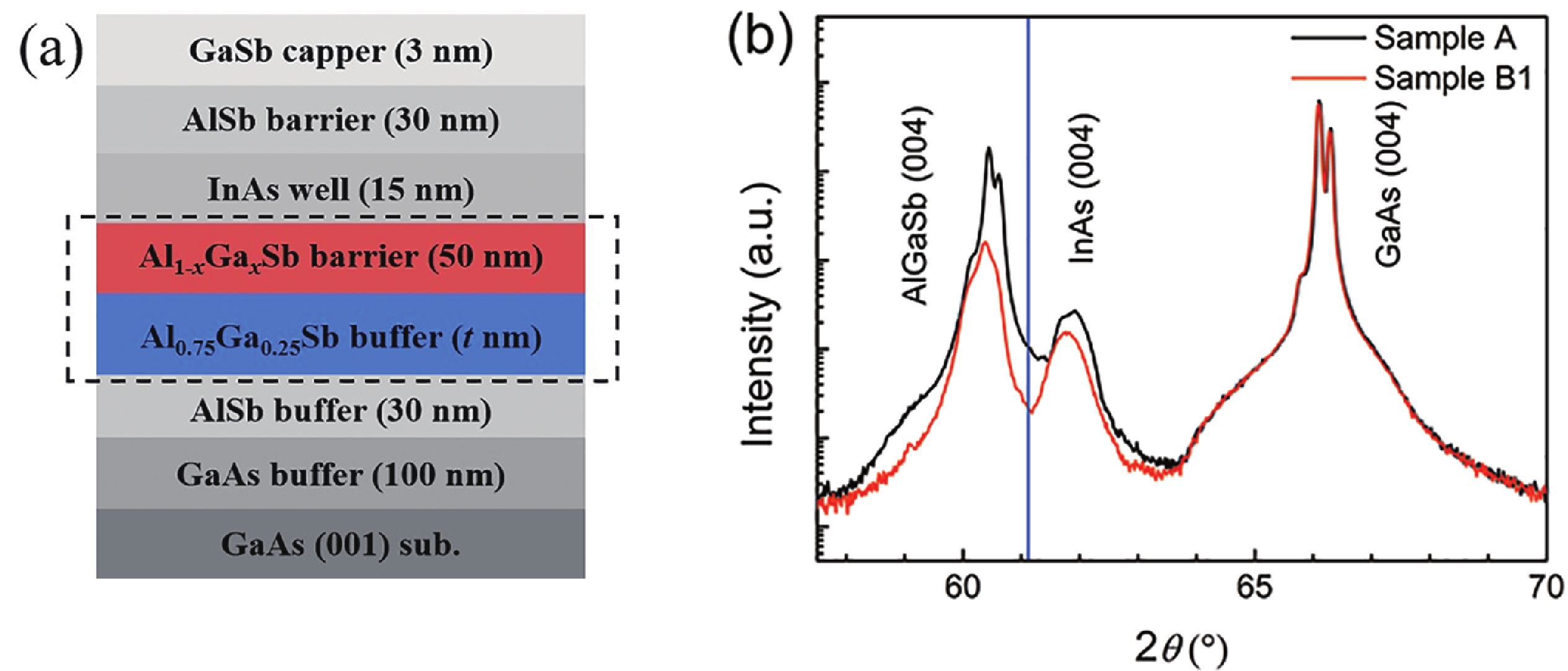
Fig. 1.  (Color online) (a) Layer structure and (b) XRD curves of (Al,Ga)Sb/InAs 2DEGs. The blue line in (b) indicates the calculated diffraction angle of unstrained InAs (004) plane.

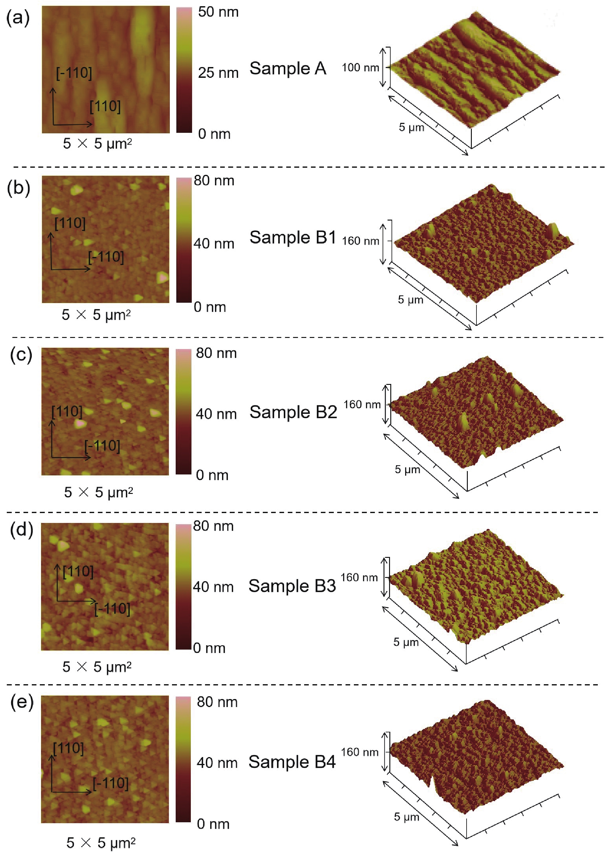
Fig. 2.  (Color online) AFM images (5 × 5 μm2) of (a) sample A, (b) sample B1, (c) sample B2, (d) sample B3, and (e) sample B4. The left-hand and right-hand images in (a)–(e) correspond to the 2D and 3D surface morphology, respectively.

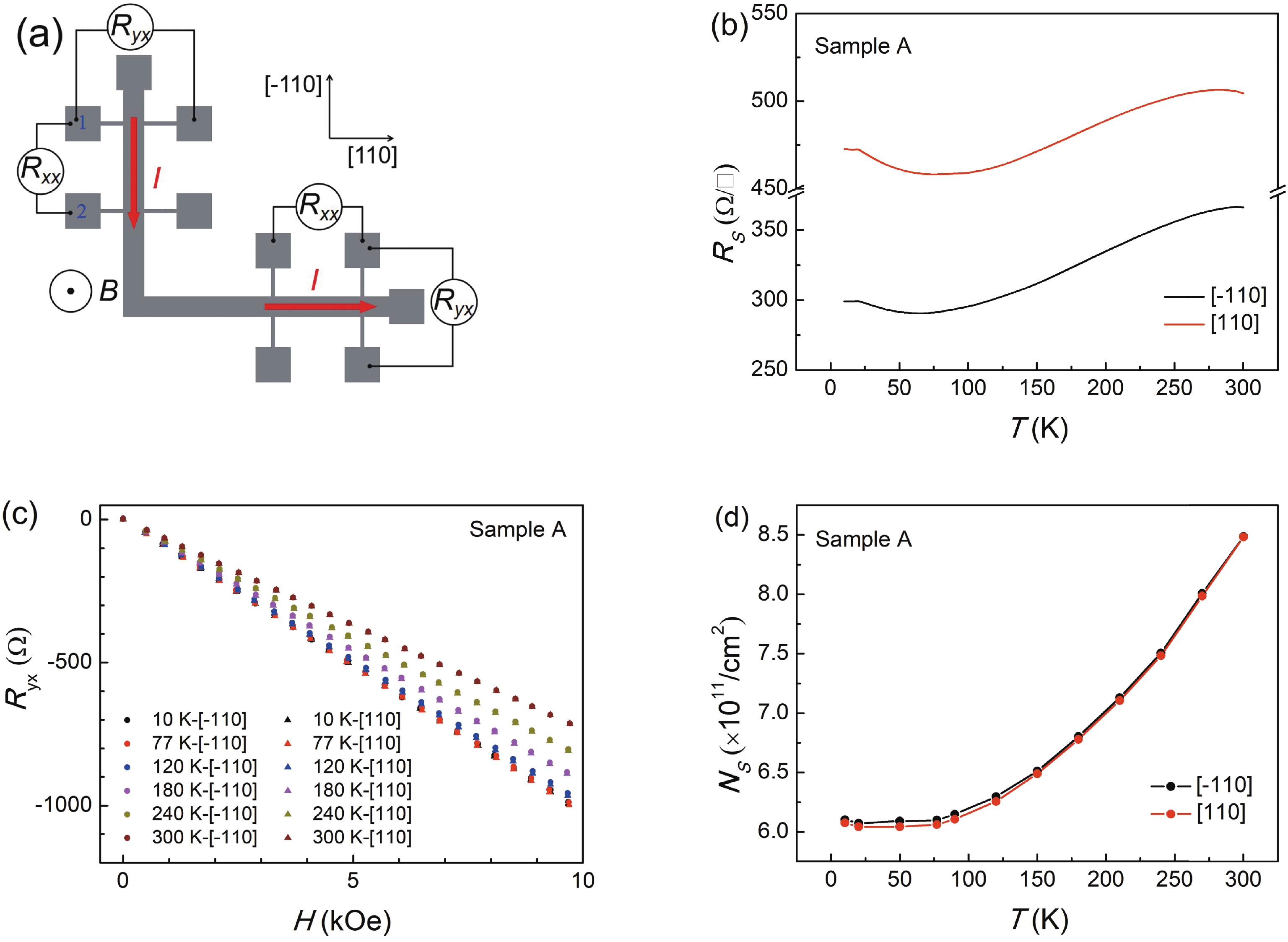
Fig. 3.  (Color online) (a) Schematic diagram of Hall bar devices with the current along the [–110] and [110] directions. (b) Sheet resistances as a function of temperature, (c) Hall resistances as a function of magnetic field, and (d) electron sheet concentrations as a function of temperature along the [–110] and [110] directions for sample A.

Fig. 4.  (Color online) (a) Temperature dependence of electron mobilities along the [–110] and [110] directions for sample A. (b) μ[–110]/μ[110] and NS[–110]/NS[110] as a function of temperature for sample A.

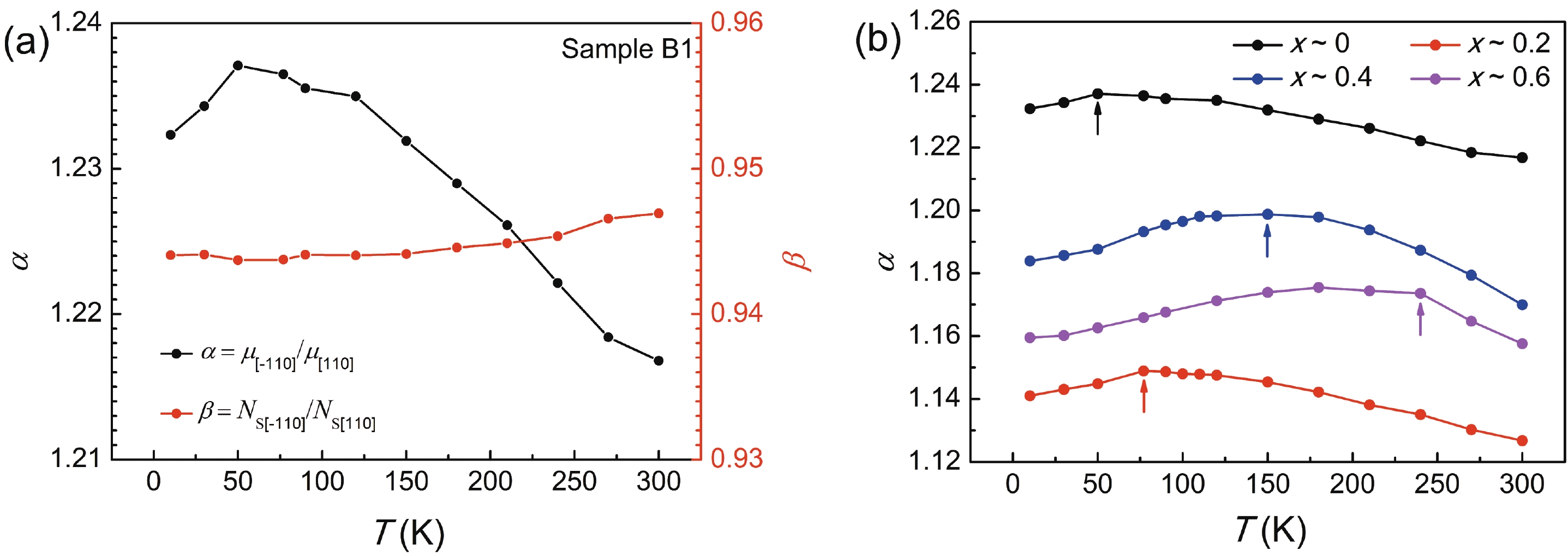
Fig. 5.  (Color online) (a) Temperature dependence of μ[–110]/μ[110] and NS[–110]/NS[110] for sample B1. (b) μ[–110]/μ[110] as a function of temperature for samples B1–B4.

Table 1.   Detailed information of A and series-B samples.

ParameterASeries-B
B1B2B3B4
t (nm)~ 1000~ 120~ 120~ 120~ 120
x~ 0~ 0~ 0.2~ 0.4~ 0.6
DownLoad: CSV
[1]
Tsui D C, Stormer H L, Gossard A C. Two-dimensional magnetotransport in the extreme quantum limit. Phys Rev Lett, 1982, 48(22), 1559 doi: 10.1103/PhysRevLett.48.1559
[2]
Willett R, Eisenstein J P, Störmer H L, et al. Observation of an even-denominator quantum number in the fractional quantum Hall effect. Phys Rev Lett, 1987, 59(15), 1776 doi: 10.1103/PhysRevLett.59.1776
[3]
Kjaergaard M, Nichele F, Suominen H J, et al. Quantized conductance doubling and hard gap in a two-dimensional semiconductor-superconductor heterostructure. Nat Commun, 2016, 7(1), 1 doi: 10.1038/ncomms12841
[4]
Shabani J, Kjærgaard M, Suominen H J, et al. Two-dimensional epitaxial superconductor-semiconductor heterostructures: A platform for topological superconducting networks. Phys Rev B, 2016, 93(15), 155402 doi: 10.1103/PhysRevB.93.155402
[5]
Lee J H, Lee J H. Enhanced output power of InGaN-based light-emitting diodes with AlGaN/GaN two-dimensional electron gas structure. IEEE Electron Device Lett, 2010, 31(5), 455 doi: 10.1109/LED.2010.2042274
[6]
Lee J H, Lee J H. High-power InGaN-based LED with tunneling-junction-induced two-dimensional electron gas at AlGaN/GaN heterostructure. IEEE Trans Electron Devices, 2011, 58(9), 3058 doi: 10.1109/TED.2011.2159119
[7]
Sandhu A, Okamoto A, Shibasaki I, et al. Nano and micro Hall-effect sensors for room-temperature scanning hall probe microscopy. Microelectron Eng, 2004, 73, 524 doi: 10.1016/j.mee.2004.03.029
[8]
Sandhu A, Masuda H, Oral A, et al. Room temperature scanning Hall probe microscopy using GaAs/AlGaAs and Bi micro-hall probes. Ultramicroscopy, 2002, 91(1), 97 doi: 10.1016/S0304-3991(02)00087-6
[9]
Kroemer H. The 6.1 Å family (InAs, GaSb, AlSb) and its heterostructures: a selective review. Physica E, 2004, 20(3), 196 doi: 10.1016/j.physe.2003.08.003
[10]
Nakagawa A, Kroemer H, English J H. Electrical properties and band offsets of InAs/AlSb n-N isotype heterojunctions grown on GaAs. Appl Phys Lett, 1989, 54(19), 1893 doi: 10.1063/1.101233
[11]
Rogalski A, Martyniuk P, Kopytko M. InAs/GaSb type-II superlattice infrared detectors: Future prospect. Appl Phys Rev, 2017, 4(3), 031304 doi: 10.1063/1.4999077
[12]
Hosoda T, Feng T, Shterengas L, et al. High power cascade diode lasers emitting near 2 μm. Appl Phys Lett, 2016, 108(13), 131109 doi: 10.1063/1.4944553
[13]
Nam Hai P, Duc Anh L, Mohan S, et al. Growth and characterization of n-type electron-induced ferromagnetic semiconductor (In, Fe) As. Appl Phys Lett, 2012, 101(18), 182403 doi: 10.1063/1.4764947
[14]
Dietl T, Bonanni A, Ohno H. Families of magnetic semiconductors-an overview. J Semicond, 2019, 40(8), 080301 doi: 10.1088/1674-4926/40/8/080301
[15]
Gu B. High temperature magnetic semiconductors: narrow band gaps and two-dimensional systems. J Semicond, 2019, 40(8), 081504 doi: 10.1088/1674-4926/40/8/081504
[16]
Boos J B, Kruppa W, Bennett B R, et al. AlSb/InAs HEMT's for low-voltage, high-speed applications. IEEE Trans Electron Devices, 1998, 45(9), 1869 doi: 10.1109/16.711349
[17]
Ma B Y, Bergman J, Chen P, et al. InAs/AlSb HEMT and its application to ultra-low-power wideband high-gain low-noise amplifiers. IEEE Trans Microwave Theory Tech, 2006, 54(12), 4448 doi: 10.1109/TMTT.2006.883604
[18]
Moschetti G, Zhao H, Nilsson P Å, et al. Anisotropic transport properties in InAs/AlSb heterostructures. Appl Phys Lett, 2010, 97(24), 243510 doi: 10.1063/1.3527971
[19]
Desplanque L, El Kazzi S, Codron J L, et al. AlSb nucleation induced anisotropic electron mobility in AlSb/InAs heterostructures on GaAs. Appl Phys Lett, 2012, 100(26), 262103 doi: 10.1063/1.4730958
[20]
Löhr S, Mendach S, Vonau T, et al. Highly anisotropic electron transport in shallow InGaAs heterostructures. Phys Rev B, 2003, 67(4), 045309 doi: 10.1103/PhysRevB.67.045309
[21]
Tokura Y, Saku T, Tarucha S, et al. Anisotropic roughness scattering at a heterostructure interface. Phys Rev B, 1992, 46(23), 15558 doi: 10.1103/PhysRevB.46.15558
[22]
Akabori M, Trinh T Q, Kudo M, et al. Strain-enhanced electron mobility anisotropy in InxGa1 – xAs/InP two-dimensional electron gases. Physica E, 2010, 42(4), 1130 doi: 10.1016/j.physe.2009.11.039
[23]
Wei Q Q, Wang H L, Tong S C, et al. Ga composition effects on the electrical parameters of (Al, Ga) Sb/InAs two-dimensional electron gas. Semicond Sci Technol, 2020, 36(2), 025002 doi: 10.1088/1361-6641/abcb1a
[24]
Goldman R S, Wieder H H, Kavanagh K L, et al. Anisotropic structural, electronic, and optical properties of InGaAs grown by molecular beam epitaxy on misoriented substrates. Appl Phys Lett, 1994, 65(11), 1424 doi: 10.1063/1.112071
[25]
Quang D N, Tuoc V N, Tung N H, et al. Random piezoelectric field in real [001]-oriented strain-relaxed semiconductor heterostructures. Phys Rev Lett, 2002, 89(7), 077601 doi: 10.1103/PhysRevLett.89.077601
[26]
Quang D N, Tuoc V N, Huan T D. Roughness-induced piezoelectric scattering in lattice-mismatched semiconductor quantum wells. Phys Rev. B, 2003, 68(19), 195316 doi: 10.1103/PhysRevB.68.195316
[27]
Anastassakis E. Strained superlattices and heterostructures: Elastic considerations. J Appl Phys, 1990, 68(9), 4561 doi: 10.1063/1.346162
[28]
Le S P, Suzuki T. Electron mobility anisotropy in InAs/GaAs (001) heterostructures. Appl Phys Lett, 2021, 118(18), 182101 doi: 10.1063/5.0039748
[29]
Saku T, Horikoshi Y, Tokura Y. Limit of electron mobility in AlGaAs/GaAs modulation-doped heterostructures. Jpn J Appl Phys, 1996, 35(1R), 34 doi: 10.1143/JJAP.35.34
[30]
Cho S, Majerfeld A, Sanz-Hervás A, et al. Determination of the pyroelectric coefficient in strained InGaAs/GaAs quantum wells grown on (111)B GaAs substrates. J Appl Phys, 2001, 90(2), 915 doi: 10.1063/1.1379563
[31]
Sanchez J J, Izpura J I, Tijero J M G, et al. Confirmation of the pyroelectric coefficient of strained InxGa1– xAs/GaAs quantum well structures grown on (111)B GaAs by differential photocurrent spectroscopy. J Appl Phys, 2002, 91(5), 3002 doi: 10.1063/1.1445278
[32]
Cho S, Majerfeld A, Sánchez J J, et al. Observation of the pyroelectric effect in strained piezoelectric InGaAs/GaAs quantum-wells grown on (111) GaAs substrates. Microelectron J, 2002, 33(7), 531 doi: 10.1016/S0026-2692(02)00014-9
[33]
Li Z H, Wang W X, Liu L S, et al. Buffer influence on AlSb/InAs/AlSb quantum wells. J Cryst Growth, 2007, 301, 181 doi: 10.1016/j.jcrysgro.2006.11.295
  • Search

    Advanced Search >>

    GET CITATION

    shu

    Export: BibTex EndNote

    Article Metrics

    Article views: 1540 Times PDF downloads: 68 Times Cited by: 0 Times

    History

    Received: 12 January 2022 Revised: 10 February 2022 Online: Accepted Manuscript: 19 April 2022Uncorrected proof: 19 April 2022Corrected proof: 19 April 2022Published: 01 July 2022

    Catalog

      Email This Article

      User name:
      Email:*请输入正确邮箱
      Code:*验证码错误
      Qiqi Wei, Hailong Wang, Xupeng Zhao, Jianhua Zhao. Electron mobility anisotropy in (Al,Ga)Sb/InAs two-dimensional electron gases epitaxied on GaAs (001) substrates[J]. Journal of Semiconductors, 2022, 43(7): 072101. doi: 10.1088/1674-4926/43/7/072101 ****Qiqi Wei, Hailong Wang, Xupeng Zhao, Jianhua Zhao, Electron mobility anisotropy in (Al,Ga)Sb/InAs two-dimensional electron gases epitaxied on GaAs (001) substrates[J]. Journal of Semiconductors, 2022, 43(7), 072101 doi: 10.1088/1674-4926/43/7/072101
      Citation:
      Qiqi Wei, Hailong Wang, Xupeng Zhao, Jianhua Zhao. Electron mobility anisotropy in (Al,Ga)Sb/InAs two-dimensional electron gases epitaxied on GaAs (001) substrates[J]. Journal of Semiconductors, 2022, 43(7): 072101. doi: 10.1088/1674-4926/43/7/072101 ****
      Qiqi Wei, Hailong Wang, Xupeng Zhao, Jianhua Zhao, Electron mobility anisotropy in (Al,Ga)Sb/InAs two-dimensional electron gases epitaxied on GaAs (001) substrates[J]. Journal of Semiconductors, 2022, 43(7), 072101 doi: 10.1088/1674-4926/43/7/072101

      Electron mobility anisotropy in (Al,Ga)Sb/InAs two-dimensional electron gases epitaxied on GaAs (001) substrates

      DOI: 10.1088/1674-4926/43/7/072101
      More Information
      • Qiqi Wei:obtained his B.Sc. degree from College of Electronic Science and Engineering at Jilin University in 2017. He then joined the State Key Laboratory of Superlattices and Microstructures under the supervision of Prof. Jianhua Zhao, and received his PhD degree in 2022. His research focuses on the growth and magneto-transport measurements of AlGaSb/InAs 2DEGs
      • Jianhua Zhao:is a professor at the Institute of Semiconductors (IoS), Chinese Academy of Sciences (CAS). She received her B.Sc. and M.Sc. degrees from Jilin University, in 1985 and 1988 respectively, and a PhD degree from the Institute of Physics, CAS in 1999. From 1999 to 2002, she was a postdoc, first at IoS, CAS, and then at Tohoku University. In 2002, she became a professor at IoS, CAS. Her current interests include semiconductor spintronics and low-dimensional semiconductor physics
      • Corresponding author: jhzhao@semi.ac.cn
      • Received Date: 2022-01-12
      • Revised Date: 2022-02-10
      • Available Online: 2022-04-19

      Catalog

        /

        DownLoad:  Full-Size Img  PowerPoint
        Return
        Return