


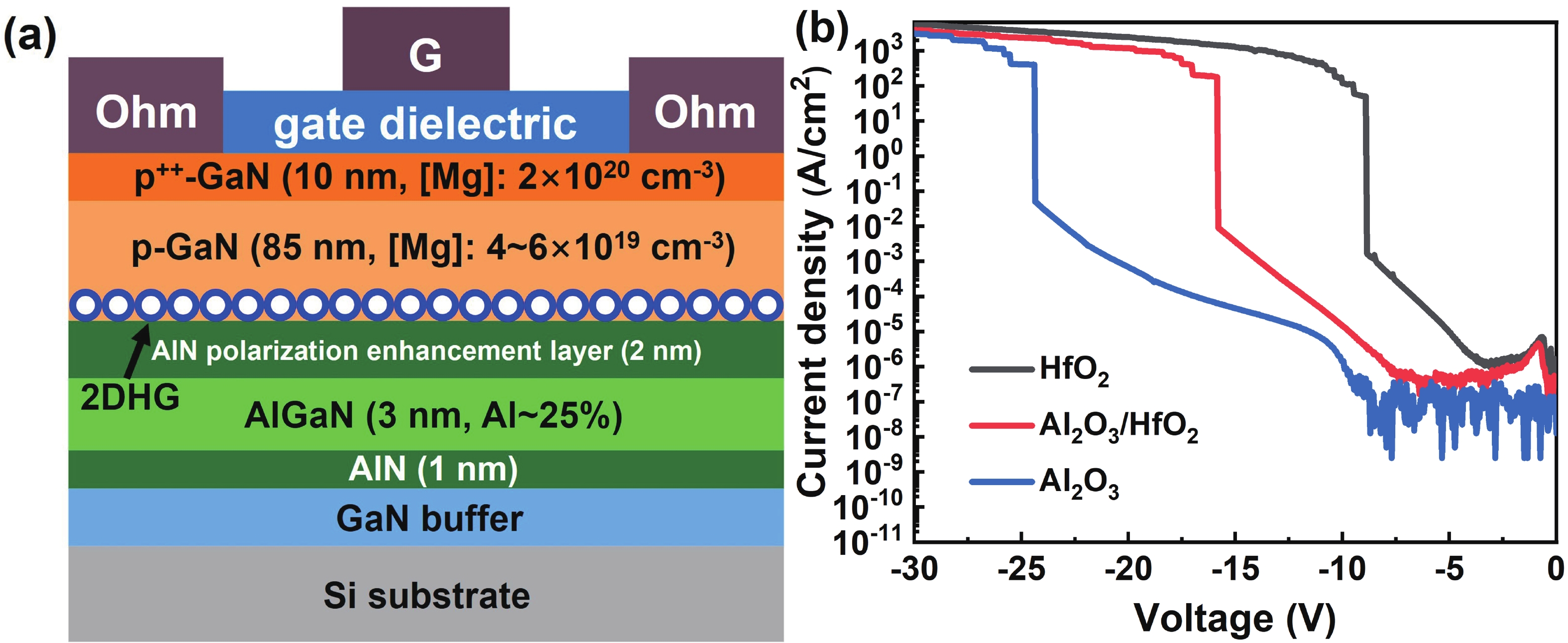
Fig. 1.
(Color online) (a) Cross-sectional schematic and (b) current density−voltage curves of the MOS device on the p++-GaN/p-GaN/AlN/AlGaN/AlN/GaN heterostructure.
ARTICLES
Hao Jin1, 2, Sen Huang1, 2, , Qimeng Jiang1, , Yingjie Wang1, 2, Jie Fan1, Haibo Yin1, 2, Xinhua Wang1, 2, Ke Wei1, 2, Jianxun Liu3, Yaozong Zhong3, Qian Sun3 and Xinyu Liu1, 2
Corresponding author: Sen Huang, huangsen@ime.ac.cn; Qimeng Jiang, jiangqimeng@ime.ac.cn
Abstract: In this letter, an enhancement-mode (E-mode) GaN p-channel field-effect transistor (p-FET) with a high current density of −4.9 mA/mm based on a O3-Al2O3/HfO2 (5/15 nm) stacked gate dielectric was demonstrated on a p++-GaN/p-GaN/AlN/AlGaN/AlN/GaN/Si heterostructure. Attributed to the p++-GaN capping layer, a good linear ohmic I−V characteristic featuring a low-contact resistivity (ρc) of 1.34 × 10⁻⁴ Ω·cm2 was obtained. High gate leakage associated with the HfO2 high-k gate dielectric was effectively blocked by the 5-nm O3-Al2O3 insertion layer grown by atomic layer deposition, contributing to a high ION/IOFF ratio of 6 × 10⁶ and a remarkably reduced subthreshold swing (SS) in the fabricated p-FETs. The proposed structure is compelling for energy-efficient GaN complementary logic (CL) circuits.
Keywords: GaN, p-FETs, enhancement-mode, HfO2, subthreshold swing
| [1] |
Hoo Teo K, Zhang Y H, Chowdhury N, et al. Emerging GaN technologies for power, RF, digital, and quantum computing applications: Recent advances and prospects. J Appl Phys, 2021, 130, 160902 doi: 10.1063/5.0061555
|
| [2] |
Wu K F, Huang S Y, Wang W L, et al. Recent progress in III-nitride nanosheets: Properties, materials and applications. Semicond Sci Technol, 2021, 36, 123002 doi: 10.1088/1361-6641/ac2c26
|
| [3] |
Jones E A, Wang F, Ozpineci B. Application-based review of GaN HFETs. 2014 IEEE Workshop on Wide Bandgap Power Devices and Applications, Knoxville, TN, USA, 2014, 24 doi: 10.1109/WiPDA.2014.6964617
|
| [4] |
Chen K J, Häberlen O, Lidow A, et al. GaN-on-Si power technology: Devices and applications. IEEE Trans Electron Devices, 2017, 64, 779 doi: 10.1109/TED.2017.2657579
|
| [5] |
Amano H, Baines Y, Beam E, et al. The 2018 GaN power electronics roadmap. J Phys D: Appl Phys, 2018, 51, 163001 doi: 10.1088/1361-6463/aaaf9d
|
| [6] |
Wang W L, Jiang H S, Li L H, et al. Two-dimensional group-III nitrides and devices: A critical review. Rep Prog Phys, 2021, 84, 086501 doi: 10.1088/1361-6633/ac11c4
|
| [7] |
Bader S J, Lee H, Chaudhuri R, et al. Prospects for wide bandgap and ultrawide bandgap CMOS devices. IEEE Trans Electron Devices, 2020, 67, 4010 doi: 10.1109/TED.2020.3010471
|
| [8] |
Götz W, Johnson N M, Walker J, et al. Activation of acceptors in Mg-doped GaN grown by metalorganic chemical vapor deposition. Appl Phys Lett, 1996, 68, 667 doi: 10.1063/1.116503
|
| [9] |
Li S J, Sun P Y, Xing Z H, et al. Degradation mechanisms of Mg-doped GaN/AlN superlattices HEMTs under electrical stress. Appl Phys Lett, 2022, 121, 062101 doi: 10.1063/5.0094957
|
| [10] |
Song J O, Ha J S, Seong T Y. Ohmic-contact technology for GaN-based light-emitting diodes: Role of P-type contact. IEEE Trans Electron Devices, 2010, 57, 42 doi: 10.1109/TED.2009.2034506
|
| [11] |
Chaudhuri R, Bader S J, Chen Z, et al. A polarization-induced 2D hole gas in undoped gallium nitride quantum wells. Science, 2019, 365(6460), 1454 doi: 10.1126/science.aau8623
|
| [12] |
Zimmermann T, Neuburger M, Kunze M, et al. P-channel InGaN-HFET structure based on polarization doping. IEEE Electron Device Lett, 2004, 25, 450 doi: 10.1109/LED.2004.830285
|
| [13] |
Hahn H, Reuters B, Pooth A, et al. P-channel enhancement and depletion mode GaN-based HFETs with quaternary backbarriers. IEEE Trans Electron Devices, 2013, 60, 3005 doi: 10.1109/TED.2013.2272330
|
| [14] |
Nakajima A, Sumida Y, Dhyani M H, et al. High density two-dimensional hole gas induced by negative polarization at GaN/AlGaN heterointerface. Appl Phys Express, 2010, 3, 121004 doi: 10.1143/APEX.3.121004
|
| [15] |
Chowdhury N, Lemettinen J, Xie Q Y, et al. P-channel GaN transistor based on p-GaN/AlGaN/GaN on Si. IEEE Electron Device Lett, 2019, 40, 1036 doi: 10.1109/LED.2019.2916253
|
| [16] |
Chowdhury N, Xie Q Y, Niroula J, et al. Field-induced acceptor ionization in enhancement-mode GaN p-MOSFETs. 2020 IEEE International Electron Devices Meeting (IEDM), 2021, 5.5. 1 doi: 10.1109/IEDM13553.2020.9371963
|
| [17] |
Chowdhury N, Xie Q Y, Palacios T. Tungsten-gated GaN/AlGaN p-FET with Imax > 120 mA/mm on GaN-on-Si. IEEE Electron Device Lett, 2022, 43, 545 doi: 10.1109/LED.2022.3149659
|
| [18] |
Chowdhury N, Xie Q Y, Yuan M Y, et al. First demonstration of a self-aligned GaN p-FET. 2019 IEEE International Electron Devices Meeting (IEDM), 2020, 4.6. 1 doi: 10.1109/IEDM19573.2019.8993569
|
| [19] |
Yin Y D, Lee K B. High-performance enhancement-mode p-channel GaN MISFETs with steep subthreshold swing. IEEE Electron Device Lett, 2022, 43, 533 doi: 10.1109/LED.2022.3152308
|
| [20] |
Bader S J, Chaudhuri R, Nomoto K, et al. Gate-recessed E-mode p-channel HFET with high on-current based on GaN/AlN 2D hole gas. IEEE Electron Device Lett, 2018, 39, 1848 doi: 10.1109/LED.2018.2874190
|
| [21] |
Chowdhury N, Xie Q Y, Yuan M Y, et al. Regrowth-free GaN-based complementary logic on a Si substrate. IEEE Electron Device Lett, 2020, 41, 820 doi: 10.1109/LED.2020.2987003
|
| [22] |
Chu R M, Cao Y, Chen M, et al. An experimental demonstration of GaN CMOS technology. IEEE Electron Device Lett, 2016, 37, 269 doi: 10.1109/LED.2016.2515103
|
| [23] |
Ma J, Yoo G. Low subthreshold swing double-gate β-Ga2O3 field-effect transistors with polycrystalline hafnium oxide dielectrics. IEEE Electron Device Lett, 2019, 40, 1317 doi: 10.1109/LED.2019.2924680
|
| [24] |
Mistry K, Allen C, Auth C, et al. A 45nm logic technology with high-k metal gate transistors, strained silicon, 9 Cu interconnect layers, 193nm dry patterning, and 100% Pb-free packaging. 2007 IEEE International Electron Devices Meeting, 2008, 247 doi: 10.1109/IEDM.2007.4418914
|
| [25] |
Huang S, Wang X H, Liu X Y, et al. An ultrathin-barrier AlGaN/GaN heterostructure: A recess-free technology for the fabrication and integration of GaN-based power devices and power-driven circuits. Semicond Sci Technol, 2021, 36, 044002 doi: 10.1088/1361-6641/abd2fe
|
| [26] |
Huang S, Liu X Y, Wei K, et al. O3-sourced atomic layer deposition of high quality Al2O3 gate dielectric for normally-off GaN metal-insulator-semiconductor high-electron-mobility transistors. Appl Phys Lett, 2015, 106, 033507 doi: 10.1063/1.4906601
|
| [27] |
Huang H H, Fang G J, Li Y, et al. Improved and color tunable electroluminescence from n-ZnO/HfO2/p-GaN heterojunction light emitting diodes. Appl Phys Lett, 2012, 100, 233502 doi: 10.1063/1.4724212
|
| [28] |
Jin H, Jiang Q M, Huang S, et al. An enhancement-mode GaN p-FET with improved breakdown voltage. IEEE Electron Device Lett, 2022, 43, 1191 doi: 10.1109/LED.2022.3184998
|
| [29] |
Guo F Q, Huang S, Wang X H, et al. Suppression of interface states between nitride-based gate dielectrics and ultrathin-barrier AlGaN/GaN heterostructure with in situ remote plasma pretreatments. Appl Phys Lett, 2021, 118, 093503 doi: 10.1063/5.0041421
|
| [30] |
Zheng Z Y, Song W J, Zhang L, et al. High ION and ION/IOFF ratio enhancement-mode buried p-channel GaN MOSFETs on p-GaN gate power HEMT platform. IEEE Electron Device Lett, 2020, 41, 26 doi: 10.1109/LED.2019.2954035
|
| [31] |
Yang C, Fu H Q, Peri P, et al. Enhancement-mode gate-recess-free GaN-based p-channel heterojunction field-effect transistor with ultra-low subthreshold swing. IEEE Electron Device Lett, 2021, 42, 1128 doi: 10.1109/LED.2021.3092040
|
| [32] |
Zheng Z Y, Song W J, Zhang L, et al. Enhancement-mode GaN p-channel MOSFETs for power integration. 2020 32nd International Symposium on Power Semiconductor Devices and ICs (ISPSD), 2020, 525 doi: 10.1109/ISPSD46842.2020.9170081
|


Article views: 2936 Times PDF downloads: 219 Times Cited by: 0 Times
Received: 10 February 2023 Revised: 27 March 2023 Online: Accepted Manuscript: 20 June 2023Uncorrected proof: 20 June 2023Corrected proof: 12 September 2023Published: 10 October 2023
| Citation: |
Hao Jin, Sen Huang, Qimeng Jiang, Yingjie Wang, Jie Fan, Haibo Yin, Xinhua Wang, Ke Wei, Jianxun Liu, Yaozong Zhong, Qian Sun, Xinyu Liu. High-performance enhancement-mode GaN-based p-FETs fabricated with O3-Al2O3/HfO2-stacked gate dielectric[J]. Journal of Semiconductors, 2023, 44(10): 102801. doi: 10.1088/1674-4926/44/10/102801
****
H Jin, S Huang, Q M Jiang, Y J Wang, J Fan, H B Yin, X H Wang, K Wei, J X Liu, Y Z Zhong, Q Sun, X Y Liu. High-performance enhancement-mode GaN-based p-FETs fabricated with O3-Al2O3/HfO2-stacked gate dielectric[J]. J. Semicond, 2023, 44(10): 102801. doi: 10.1088/1674-4926/44/10/102801

|
 Hao Jin:received his MS degree from the Beijing Institute of Technology, Beijing, China, in 2020. He is pursuing a PhD degree at the Institute of Microelectronics, Chinese Academy of Science, Beijing. His research focuses on fabrication and monolithic integration of GaN devices
 Sen Huang:received his PhD degree from Peking University, Beijing, China, in 2009. He is currently a professor with the Institute of Microelectronics, Chinese Academy of Sciences, Beijing. His current research interests include advanced design, fabrication, and characterization technologies for III–V power semiconductor or devices
 Qimeng Jiang:received his PhD degree from The Hong Kong University of Science and Technology, Hong Kong, China, in 2015. He is currently a professor with the Institute of Microelectronics, Chinese Academy of Sciences, Beijing. His current research interests include advanced design and fabrication technologies for power semiconductor devices and ICs
| [1] |
Hoo Teo K, Zhang Y H, Chowdhury N, et al. Emerging GaN technologies for power, RF, digital, and quantum computing applications: Recent advances and prospects. J Appl Phys, 2021, 130, 160902 doi: 10.1063/5.0061555
|
| [2] |
Wu K F, Huang S Y, Wang W L, et al. Recent progress in III-nitride nanosheets: Properties, materials and applications. Semicond Sci Technol, 2021, 36, 123002 doi: 10.1088/1361-6641/ac2c26
|
| [3] |
Jones E A, Wang F, Ozpineci B. Application-based review of GaN HFETs. 2014 IEEE Workshop on Wide Bandgap Power Devices and Applications, Knoxville, TN, USA, 2014, 24 doi: 10.1109/WiPDA.2014.6964617
|
| [4] |
Chen K J, Häberlen O, Lidow A, et al. GaN-on-Si power technology: Devices and applications. IEEE Trans Electron Devices, 2017, 64, 779 doi: 10.1109/TED.2017.2657579
|
| [5] |
Amano H, Baines Y, Beam E, et al. The 2018 GaN power electronics roadmap. J Phys D: Appl Phys, 2018, 51, 163001 doi: 10.1088/1361-6463/aaaf9d
|
| [6] |
Wang W L, Jiang H S, Li L H, et al. Two-dimensional group-III nitrides and devices: A critical review. Rep Prog Phys, 2021, 84, 086501 doi: 10.1088/1361-6633/ac11c4
|
| [7] |
Bader S J, Lee H, Chaudhuri R, et al. Prospects for wide bandgap and ultrawide bandgap CMOS devices. IEEE Trans Electron Devices, 2020, 67, 4010 doi: 10.1109/TED.2020.3010471
|
| [8] |
Götz W, Johnson N M, Walker J, et al. Activation of acceptors in Mg-doped GaN grown by metalorganic chemical vapor deposition. Appl Phys Lett, 1996, 68, 667 doi: 10.1063/1.116503
|
| [9] |
Li S J, Sun P Y, Xing Z H, et al. Degradation mechanisms of Mg-doped GaN/AlN superlattices HEMTs under electrical stress. Appl Phys Lett, 2022, 121, 062101 doi: 10.1063/5.0094957
|
| [10] |
Song J O, Ha J S, Seong T Y. Ohmic-contact technology for GaN-based light-emitting diodes: Role of P-type contact. IEEE Trans Electron Devices, 2010, 57, 42 doi: 10.1109/TED.2009.2034506
|
| [11] |
Chaudhuri R, Bader S J, Chen Z, et al. A polarization-induced 2D hole gas in undoped gallium nitride quantum wells. Science, 2019, 365(6460), 1454 doi: 10.1126/science.aau8623
|
| [12] |
Zimmermann T, Neuburger M, Kunze M, et al. P-channel InGaN-HFET structure based on polarization doping. IEEE Electron Device Lett, 2004, 25, 450 doi: 10.1109/LED.2004.830285
|
| [13] |
Hahn H, Reuters B, Pooth A, et al. P-channel enhancement and depletion mode GaN-based HFETs with quaternary backbarriers. IEEE Trans Electron Devices, 2013, 60, 3005 doi: 10.1109/TED.2013.2272330
|
| [14] |
Nakajima A, Sumida Y, Dhyani M H, et al. High density two-dimensional hole gas induced by negative polarization at GaN/AlGaN heterointerface. Appl Phys Express, 2010, 3, 121004 doi: 10.1143/APEX.3.121004
|
| [15] |
Chowdhury N, Lemettinen J, Xie Q Y, et al. P-channel GaN transistor based on p-GaN/AlGaN/GaN on Si. IEEE Electron Device Lett, 2019, 40, 1036 doi: 10.1109/LED.2019.2916253
|
| [16] |
Chowdhury N, Xie Q Y, Niroula J, et al. Field-induced acceptor ionization in enhancement-mode GaN p-MOSFETs. 2020 IEEE International Electron Devices Meeting (IEDM), 2021, 5.5. 1 doi: 10.1109/IEDM13553.2020.9371963
|
| [17] |
Chowdhury N, Xie Q Y, Palacios T. Tungsten-gated GaN/AlGaN p-FET with Imax > 120 mA/mm on GaN-on-Si. IEEE Electron Device Lett, 2022, 43, 545 doi: 10.1109/LED.2022.3149659
|
| [18] |
Chowdhury N, Xie Q Y, Yuan M Y, et al. First demonstration of a self-aligned GaN p-FET. 2019 IEEE International Electron Devices Meeting (IEDM), 2020, 4.6. 1 doi: 10.1109/IEDM19573.2019.8993569
|
| [19] |
Yin Y D, Lee K B. High-performance enhancement-mode p-channel GaN MISFETs with steep subthreshold swing. IEEE Electron Device Lett, 2022, 43, 533 doi: 10.1109/LED.2022.3152308
|
| [20] |
Bader S J, Chaudhuri R, Nomoto K, et al. Gate-recessed E-mode p-channel HFET with high on-current based on GaN/AlN 2D hole gas. IEEE Electron Device Lett, 2018, 39, 1848 doi: 10.1109/LED.2018.2874190
|
| [21] |
Chowdhury N, Xie Q Y, Yuan M Y, et al. Regrowth-free GaN-based complementary logic on a Si substrate. IEEE Electron Device Lett, 2020, 41, 820 doi: 10.1109/LED.2020.2987003
|
| [22] |
Chu R M, Cao Y, Chen M, et al. An experimental demonstration of GaN CMOS technology. IEEE Electron Device Lett, 2016, 37, 269 doi: 10.1109/LED.2016.2515103
|
| [23] |
Ma J, Yoo G. Low subthreshold swing double-gate β-Ga2O3 field-effect transistors with polycrystalline hafnium oxide dielectrics. IEEE Electron Device Lett, 2019, 40, 1317 doi: 10.1109/LED.2019.2924680
|
| [24] |
Mistry K, Allen C, Auth C, et al. A 45nm logic technology with high-k metal gate transistors, strained silicon, 9 Cu interconnect layers, 193nm dry patterning, and 100% Pb-free packaging. 2007 IEEE International Electron Devices Meeting, 2008, 247 doi: 10.1109/IEDM.2007.4418914
|
| [25] |
Huang S, Wang X H, Liu X Y, et al. An ultrathin-barrier AlGaN/GaN heterostructure: A recess-free technology for the fabrication and integration of GaN-based power devices and power-driven circuits. Semicond Sci Technol, 2021, 36, 044002 doi: 10.1088/1361-6641/abd2fe
|
| [26] |
Huang S, Liu X Y, Wei K, et al. O3-sourced atomic layer deposition of high quality Al2O3 gate dielectric for normally-off GaN metal-insulator-semiconductor high-electron-mobility transistors. Appl Phys Lett, 2015, 106, 033507 doi: 10.1063/1.4906601
|
| [27] |
Huang H H, Fang G J, Li Y, et al. Improved and color tunable electroluminescence from n-ZnO/HfO2/p-GaN heterojunction light emitting diodes. Appl Phys Lett, 2012, 100, 233502 doi: 10.1063/1.4724212
|
| [28] |
Jin H, Jiang Q M, Huang S, et al. An enhancement-mode GaN p-FET with improved breakdown voltage. IEEE Electron Device Lett, 2022, 43, 1191 doi: 10.1109/LED.2022.3184998
|
| [29] |
Guo F Q, Huang S, Wang X H, et al. Suppression of interface states between nitride-based gate dielectrics and ultrathin-barrier AlGaN/GaN heterostructure with in situ remote plasma pretreatments. Appl Phys Lett, 2021, 118, 093503 doi: 10.1063/5.0041421
|
| [30] |
Zheng Z Y, Song W J, Zhang L, et al. High ION and ION/IOFF ratio enhancement-mode buried p-channel GaN MOSFETs on p-GaN gate power HEMT platform. IEEE Electron Device Lett, 2020, 41, 26 doi: 10.1109/LED.2019.2954035
|
| [31] |
Yang C, Fu H Q, Peri P, et al. Enhancement-mode gate-recess-free GaN-based p-channel heterojunction field-effect transistor with ultra-low subthreshold swing. IEEE Electron Device Lett, 2021, 42, 1128 doi: 10.1109/LED.2021.3092040
|
| [32] |
Zheng Z Y, Song W J, Zhang L, et al. Enhancement-mode GaN p-channel MOSFETs for power integration. 2020 32nd International Symposium on Power Semiconductor Devices and ICs (ISPSD), 2020, 525 doi: 10.1109/ISPSD46842.2020.9170081
|

 WeChat ID
Journal of Semiconductors © 2017 All Rights Reserved 京ICP备05085259号-2

 DownLoad:

