J. Semicond. > 2020, Volume 41 > Issue 8 > 082006

ARTICLES

First-principle study of puckered arsenene MOSFET

Hengze Qu, Ziwei Lin, Ruijuan Guo, Xiyu Ming, Wenhan Zhou, Shiying Guo, Xiufeng Song, Shengli Zhang and Haibo Zeng

+ Author Affiliations

 Corresponding author: Shengli Zhang, Email: zhangslvip@njust.edu.cn; Haibo Zeng, zeng.haibo@njust.edu.cn

DOI: 10.1088/1674-4926/41/8/082006

PDF

Turn off MathJax

Abstract: 
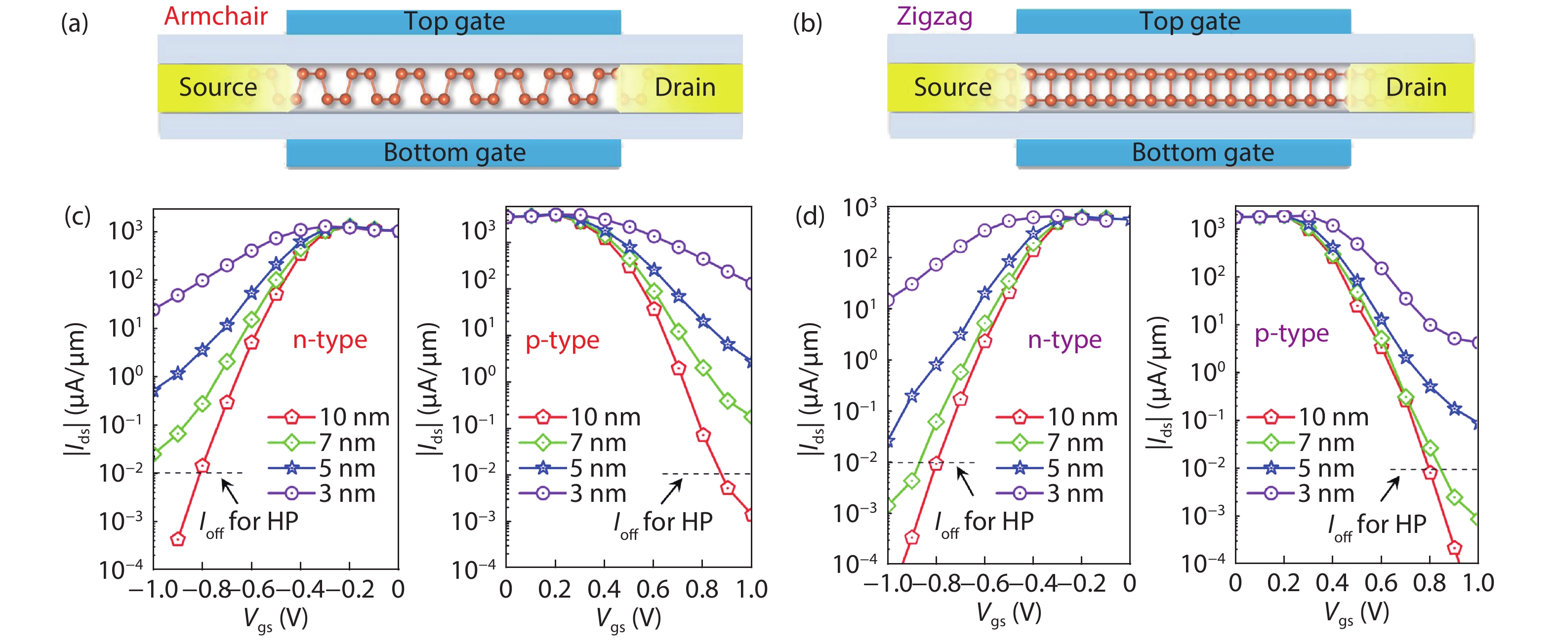
Two-dimensional material has been regarded as a competitive silicon-alternative with a gate length approaching sub-10 nm, due to its unique atomic thickness and outstanding electronic properties. Herein, we provide a comprehensively study on the electronic and ballistic transport properties of the puckered arsenene by the density functional theory coupled with nonequilibrium Green’s function formalism. The puckered arsenene exhibits an anisotropic characteristic, as effective mass for the electron/hole in the armchair and zigzag directions is 0.35/0.16 m0 and 1.26/0.32 m0. And it also holds a high electron mobility, as the highest value can reach 20 045 cm2V–1s–1. Moreover, the puckered arsenene FETs with a 10-nm channel length possess high on/off ratio above 105 and a steep subthreshold swing below 75 mV/dec, which have the potential to design high-performance electronic devices. Interestingly, the channel length limit for arsenene FETs can reach 7-nm. Furthermore, the benchmarking of the intrinsic arsenene FETs and the 32-bit arithmetic logic unit circuits also shows that the devices possess high switching speed and low energy dissipation, which can be comparable to the CMOS technologies and other CMOS alternatives. Therefore, the puckered arsenene is an attractive channel material in next-generation electronics.

Key words: first principletwo-dimensional materialelectronic propertiesarseneneMOSFET


[1]
Chau R, Doyle B, Datta S, et al. Integrated nanoelectronics for the future. Nat Mater, 2007, 6, 810 doi: 10.1038/nmat2014
[2]
Franklin A D. Nanomaterials in transistors: From high-performance to thin-film applications. Science, 2015, 349, aab2750 doi: 10.1126/science.aab2750
[3]
Desai S B, Madhvapathy S R, Sachid A B, et al. MoS2 transistors with 1-nanometer gate lengths. Science, 2016, 354, 99 doi: 10.1126/science.aah4698
[4]
Zhang S L, Guo S Y, Chen Z F, et al. Recent progress in 2D group-VA semiconductors: From theory to experiment. Chem Soc Rev, 2018, 47, 982 doi: 10.1039/C7CS00125H
[5]
Guo S Y, Zhang Y P, Ge Y Q, et al. 2D V-V binary materials: Status and challenges. Adv Mater, 2019, 31, 1902352 doi: 10.1002/adma.201902352
[6]
Zhou W H, Zhang S L, Guo S Y, et al. Designing sub-10-nm metal-oxide-semiconductor field-effect transistors via ballistic transport and disparate effective mass: The case of two-dimensional BiN. Phys Rev Appl, 2020, 13, 044066 doi: 10.1103/PhysRevApplied.13.044066
[7]
Cao W, Kang J H, Sarkar D, et al. 2D semiconductor FETs: Projections and design for sub-10 nm VLSI. IEEE Trans Electron Devices, 2015, 62, 3459 doi: 10.1109/TED.2015.2443039
[8]
Zhu Z L, Cai X L, Yi S, et al. Multivalency-driven formation of Te-based monolayer materials: A combined first-principles and experimental study. Phys Rev Lett, 2017, 119, 106101 doi: 10.1103/PhysRevLett.119.106101
[9]
Zhou Z Q, Cui Y, Tan P H, et al. Optical and electrical properties of two-dimensional anisotropic materials. J Semicond, 2019, 40, 061001 doi: 10.1088/1674-4926/40/6/061001
[10]
Zhou W H, Chen J Y, Bai P X, et al. Two-dimensional pnictogen for field-effect transistors. Res Wash D C, 2019, 2019, 1046329 doi: 10.34133/2019/1046329
[11]
Novoselov K S, Mishchenko A, Carvalho A, et al. 2D materials and van der Waals heterostructures. Science, 2016, 353, aac9439 doi: 10.1126/science.aac9439
[12]
Wang S X, Yu Z H, Wang X R. Electrical contacts to two-dimensional transition-metal dichalcogenides. J Semicond, 2018, 39, 124001 doi: 10.1088/1674-4926/39/12/124001
[13]
Schwierz F. Graphene transistors. Nat Nanotechnol, 2010, 5, 487 doi: 10.1038/nnano.2010.89
[14]
Tao L, Cinquanta E, Chiappe D, et al. Silicene field-effect transistors operating at room temperature. Nat Nanotechnol, 2015, 10, 227 doi: 10.1038/nnano.2014.325
[15]
Nourbakhsh A, Zubair A, Sajjad R N, et al. MoS2 field-effect transistor with sub-10 nm channel length. Nano Lett, 2016, 16, 7798 doi: 10.1021/acs.nanolett.6b03999
[16]
Qiao J S, Kong X H, Hu Z X, et al. High-mobility transport anisotropy and linear dichroism in few-layer black phosphorus. Nat Commun, 2014, 5, 4475 doi: 10.1038/ncomms5475
[17]
Zhang S L, Yan Z, Li Y F, et al. Atomically thin arsenene and antimonene: Semimetal –semiconductor and indirect-direct band-gap transitions. Angew Chem Int Ed, 2015, 54, 3112 doi: 10.1002/anie.201411246
[18]
Li L K, Yu Y J, Ye G J, et al. Black phosphorus field-effect transistors. Nat Nanotechnol, 2014, 9, 372 doi: 10.1038/nnano.2014.35
[19]
Wang X X, Hu Y, Mo J B, et al. Arsenene: A potential therapeutic agent for acute promyelocytic leukaemia cells by acting on nuclear proteins. Angew Chem Int Ed, 2020, 59, 5151 doi: 10.1002/anie.201913675
[20]
Zhong M Z, Xia Q L, Pan L F, et al. Thickness-dependent carrier transport characteristics of a new 2D elemental semiconductor: Black arsenic. Adv Funct Mater, 2018, 28, 1802581 doi: 10.1002/adfm.201802581
[21]
Wu X, Shao Y, Liu H, et al. Epitaxial growth and air-stability of monolayer antimonene on PdTe2. Adv Mater, 2017, 29, 1605407 doi: 10.1002/adma.201605407
[22]
Chen Y B, Chen C Y, Kealhofer R, et al. Black arsenic: A layered semiconductor with extreme in-plane anisotropy. Adv Mater, 2018, 30, 1800754 doi: 10.1002/adma.201800754
[23]
Pizzi G, Gibertini M, Dib E, et al. Performance of arsenene and antimonene double-gate MOSFETs from first principles. Nat Commun, 2016, 7, 12585 doi: 10.1038/ncomms12585
[24]
Quhe R G, Li Q H, Zhang Q X, et al. Simulations of quantum transport in sub-5-nm monolayer phosphorene transistors. Phys Rev Appl, 2018, 10, 024022 doi: 10.1103/PhysRevApplied.10.024022
[25]
Wang J, Cai Q, Lei J M, et al. Performance of monolayer blue phosphorene double-gate MOSFETs from the first principles. ACS Appl Mater Interfaces, 2019, 11, 20956 doi: 10.1021/acsami.9b02192
[26]
Wang Y Y, Huang P, Ye M, et al. Many-body effect, carrier mobility, and device performance of hexagonal arsenene and antimonene. Chem Mater, 2017, 29, 2191 doi: 10.1021/acs.chemmater.6b04909
[27]
Kresse G, Furthmüller J. Efficient iterative schemes forab initiototal-energy calculations using a plane-wave basis set. Phys Rev B, 1996, 54, 11169 doi: 10.1103/PhysRevB.54.11169
[28]
Perdew J P, Burke K, Ernzerhof M. Generalized gradient approximation made simple. Phys Rev Lett, 1996, 77, 3865 doi: 10.1103/PhysRevLett.77.3865
[29]
Grimme S, Ehrlich S, Goerigk L. Effect of the damping function in dispersion corrected density functional theory. J Comput Chem, 2011, 32, 1456 doi: 10.1002/jcc.21759
[30]
Takagi S, Toriumi A, Iwase M, et al. On the universality of inversion layer mobility in Si MOSFET's: Part II-effects of surface orientation. IEEE Trans Electron Devices, 1994, 41, 2363 doi: 10.1109/16.337450
[31]
Atomistix Toolkit vertion 2019.03, Synopsys QuantumWise A/S
[32]
Datta S. Quantum transport: atom to transistor. Cambridge: Cambridge University Press, 2005
[33]
Gaddemane G, Vandenberghe W G, van de Put M L, et al. Theoretical studies of electronic transport in monolayer and bilayer phosphorene: A critical overview. Phys Rev B, 2018, 98, 115416 doi: 10.1103/PhysRevB.98.115416
[34]
Poncé S, Margine E R, Giustino F. Towards predictive many-body calculations of phonon-limited carrier mobilities in semiconductors. Phys Rev B, 2018, 97, 121201 doi: 10.1103/PhysRevB.97.121201
[35]
International Roadmap for Devices and Systems, 2018 edition. https://irds.ieee.org/editions/2018 (accessed May 20, 2019)
[36]
Nikonov D E, Young I A. Overview of beyond-CMOS devices and a uniform methodology for their benchmarking. Proc IEEE, 2013, 101, 2498 doi: 10.1109/JPROC.2013.2252317
[37]
Nikonov D E, Young I A. Benchmarking of beyond-CMOS exploratory devices for logic integrated circuits. IEEE J Explor Solid-State Comput Devices Circuits, 2015, 1, 3 doi: 10.1109/JXCDC.2015.2418033
Fig. 1.  (Color online) (a) The top and side views of puckered arsenene. (b) The band structure at PBE (purple line) and HSE06 (orange line) level and the orbital-projected density of states of the puckered arsenene. (c) The partial charge density of CBM and VBM.

Fig. 2.  (Color online) The band dispersions of the CBM along (a) the armchair direction and (b) the zigzag direction, and that of VBM along (c) the armchair direction and (d) the zigzag direction. The corresponding effective mass and carrier mobility are also marked out.

Fig. 3.  (Color online) The schematic model of dual-gated puckered arsenene MOSFET along (a) the armchair and (c) zigzag direction. The transfer characteristics for puckered arsenene n- and p-MOSFETs along (b) the armchair and (d) zigzag direction with Lch = 3–10 nm.

Fig. 4.  (Color online) The SS and the on/off ratio as a function of the Lch for the puckered arsenene assessed according to the IRDS requirements for HP applications.

Fig. 5.  (Color online) The position resolved LDOS and spectral currents of puckered arsenene n-FETs with 5-nm Lch with the transport direction along (a) armchair and (b) zigzag direction as Vgs = –1 V. The position resolved LDOS and spectral current of 5-nm-Lch P-FETs along (c) the armchair and (d) zigzag directions as Vgs = 0.9 V.

Fig. 6.  (Color online) Switching energy versus delay time, τ, for a 32-bit ALU based on puckered arsenene FETs in HP conditions.

[1]
Chau R, Doyle B, Datta S, et al. Integrated nanoelectronics for the future. Nat Mater, 2007, 6, 810 doi: 10.1038/nmat2014
[2]
Franklin A D. Nanomaterials in transistors: From high-performance to thin-film applications. Science, 2015, 349, aab2750 doi: 10.1126/science.aab2750
[3]
Desai S B, Madhvapathy S R, Sachid A B, et al. MoS2 transistors with 1-nanometer gate lengths. Science, 2016, 354, 99 doi: 10.1126/science.aah4698
[4]
Zhang S L, Guo S Y, Chen Z F, et al. Recent progress in 2D group-VA semiconductors: From theory to experiment. Chem Soc Rev, 2018, 47, 982 doi: 10.1039/C7CS00125H
[5]
Guo S Y, Zhang Y P, Ge Y Q, et al. 2D V-V binary materials: Status and challenges. Adv Mater, 2019, 31, 1902352 doi: 10.1002/adma.201902352
[6]
Zhou W H, Zhang S L, Guo S Y, et al. Designing sub-10-nm metal-oxide-semiconductor field-effect transistors via ballistic transport and disparate effective mass: The case of two-dimensional BiN. Phys Rev Appl, 2020, 13, 044066 doi: 10.1103/PhysRevApplied.13.044066
[7]
Cao W, Kang J H, Sarkar D, et al. 2D semiconductor FETs: Projections and design for sub-10 nm VLSI. IEEE Trans Electron Devices, 2015, 62, 3459 doi: 10.1109/TED.2015.2443039
[8]
Zhu Z L, Cai X L, Yi S, et al. Multivalency-driven formation of Te-based monolayer materials: A combined first-principles and experimental study. Phys Rev Lett, 2017, 119, 106101 doi: 10.1103/PhysRevLett.119.106101
[9]
Zhou Z Q, Cui Y, Tan P H, et al. Optical and electrical properties of two-dimensional anisotropic materials. J Semicond, 2019, 40, 061001 doi: 10.1088/1674-4926/40/6/061001
[10]
Zhou W H, Chen J Y, Bai P X, et al. Two-dimensional pnictogen for field-effect transistors. Res Wash D C, 2019, 2019, 1046329 doi: 10.34133/2019/1046329
[11]
Novoselov K S, Mishchenko A, Carvalho A, et al. 2D materials and van der Waals heterostructures. Science, 2016, 353, aac9439 doi: 10.1126/science.aac9439
[12]
Wang S X, Yu Z H, Wang X R. Electrical contacts to two-dimensional transition-metal dichalcogenides. J Semicond, 2018, 39, 124001 doi: 10.1088/1674-4926/39/12/124001
[13]
Schwierz F. Graphene transistors. Nat Nanotechnol, 2010, 5, 487 doi: 10.1038/nnano.2010.89
[14]
Tao L, Cinquanta E, Chiappe D, et al. Silicene field-effect transistors operating at room temperature. Nat Nanotechnol, 2015, 10, 227 doi: 10.1038/nnano.2014.325
[15]
Nourbakhsh A, Zubair A, Sajjad R N, et al. MoS2 field-effect transistor with sub-10 nm channel length. Nano Lett, 2016, 16, 7798 doi: 10.1021/acs.nanolett.6b03999
[16]
Qiao J S, Kong X H, Hu Z X, et al. High-mobility transport anisotropy and linear dichroism in few-layer black phosphorus. Nat Commun, 2014, 5, 4475 doi: 10.1038/ncomms5475
[17]
Zhang S L, Yan Z, Li Y F, et al. Atomically thin arsenene and antimonene: Semimetal –semiconductor and indirect-direct band-gap transitions. Angew Chem Int Ed, 2015, 54, 3112 doi: 10.1002/anie.201411246
[18]
Li L K, Yu Y J, Ye G J, et al. Black phosphorus field-effect transistors. Nat Nanotechnol, 2014, 9, 372 doi: 10.1038/nnano.2014.35
[19]
Wang X X, Hu Y, Mo J B, et al. Arsenene: A potential therapeutic agent for acute promyelocytic leukaemia cells by acting on nuclear proteins. Angew Chem Int Ed, 2020, 59, 5151 doi: 10.1002/anie.201913675
[20]
Zhong M Z, Xia Q L, Pan L F, et al. Thickness-dependent carrier transport characteristics of a new 2D elemental semiconductor: Black arsenic. Adv Funct Mater, 2018, 28, 1802581 doi: 10.1002/adfm.201802581
[21]
Wu X, Shao Y, Liu H, et al. Epitaxial growth and air-stability of monolayer antimonene on PdTe2. Adv Mater, 2017, 29, 1605407 doi: 10.1002/adma.201605407
[22]
Chen Y B, Chen C Y, Kealhofer R, et al. Black arsenic: A layered semiconductor with extreme in-plane anisotropy. Adv Mater, 2018, 30, 1800754 doi: 10.1002/adma.201800754
[23]
Pizzi G, Gibertini M, Dib E, et al. Performance of arsenene and antimonene double-gate MOSFETs from first principles. Nat Commun, 2016, 7, 12585 doi: 10.1038/ncomms12585
[24]
Quhe R G, Li Q H, Zhang Q X, et al. Simulations of quantum transport in sub-5-nm monolayer phosphorene transistors. Phys Rev Appl, 2018, 10, 024022 doi: 10.1103/PhysRevApplied.10.024022
[25]
Wang J, Cai Q, Lei J M, et al. Performance of monolayer blue phosphorene double-gate MOSFETs from the first principles. ACS Appl Mater Interfaces, 2019, 11, 20956 doi: 10.1021/acsami.9b02192
[26]
Wang Y Y, Huang P, Ye M, et al. Many-body effect, carrier mobility, and device performance of hexagonal arsenene and antimonene. Chem Mater, 2017, 29, 2191 doi: 10.1021/acs.chemmater.6b04909
[27]
Kresse G, Furthmüller J. Efficient iterative schemes forab initiototal-energy calculations using a plane-wave basis set. Phys Rev B, 1996, 54, 11169 doi: 10.1103/PhysRevB.54.11169
[28]
Perdew J P, Burke K, Ernzerhof M. Generalized gradient approximation made simple. Phys Rev Lett, 1996, 77, 3865 doi: 10.1103/PhysRevLett.77.3865
[29]
Grimme S, Ehrlich S, Goerigk L. Effect of the damping function in dispersion corrected density functional theory. J Comput Chem, 2011, 32, 1456 doi: 10.1002/jcc.21759
[30]
Takagi S, Toriumi A, Iwase M, et al. On the universality of inversion layer mobility in Si MOSFET's: Part II-effects of surface orientation. IEEE Trans Electron Devices, 1994, 41, 2363 doi: 10.1109/16.337450
[31]
Atomistix Toolkit vertion 2019.03, Synopsys QuantumWise A/S
[32]
Datta S. Quantum transport: atom to transistor. Cambridge: Cambridge University Press, 2005
[33]
Gaddemane G, Vandenberghe W G, van de Put M L, et al. Theoretical studies of electronic transport in monolayer and bilayer phosphorene: A critical overview. Phys Rev B, 2018, 98, 115416 doi: 10.1103/PhysRevB.98.115416
[34]
Poncé S, Margine E R, Giustino F. Towards predictive many-body calculations of phonon-limited carrier mobilities in semiconductors. Phys Rev B, 2018, 97, 121201 doi: 10.1103/PhysRevB.97.121201
[35]
International Roadmap for Devices and Systems, 2018 edition. https://irds.ieee.org/editions/2018 (accessed May 20, 2019)
[36]
Nikonov D E, Young I A. Overview of beyond-CMOS devices and a uniform methodology for their benchmarking. Proc IEEE, 2013, 101, 2498 doi: 10.1109/JPROC.2013.2252317
[37]
Nikonov D E, Young I A. Benchmarking of beyond-CMOS exploratory devices for logic integrated circuits. IEEE J Explor Solid-State Comput Devices Circuits, 2015, 1, 3 doi: 10.1109/JXCDC.2015.2418033
1

A compact two-dimensional analytical model of the electrical characteristics of a triple-material double-gate tunneling FET structure

C. Usha, P. Vimala

Journal of Semiconductors, 2019, 40(12): 122901. doi: 10.1088/1674-4926/40/12/122901

2

The electronic and magnetic properties of wurtzite Mn:CdS, Cr:CdS and Mn:Cr:CdS: first principles calculations

Azeem Nabi, Zarmeena Akhtar, Tahir Iqbal, Atif Ali, Arshad Javid, et al.

Journal of Semiconductors, 2017, 38(7): 073001. doi: 10.1088/1674-4926/38/7/073001

3

Influences of ICP etching damages on the electronic properties of metal field plate 4H-SiC Schottky diodes

Hui Wang, Yingxi Niu, Fei Yang, Yong Cai, Zehong Zhang, et al.

Journal of Semiconductors, 2015, 36(10): 104006. doi: 10.1088/1674-4926/36/10/104006

4

Effects of defects on the electronic properties of WTe2 armchair nanoribbons

Bahniman Ghosh, Abhishek Gupta, Bhupesh Bishnoi

Journal of Semiconductors, 2014, 35(11): 113002. doi: 10.1088/1674-4926/35/11/113002

5

Comparative study of leakage power in CNTFET over MOSFET device

Sanjeet Kumar Sinha, Saurabh Chaudhury

Journal of Semiconductors, 2014, 35(11): 114002. doi: 10.1088/1674-4926/35/11/114002

6

In situ TEM/SEM electronic/mechanical characterization of nano material with MEMS chip

Yuelin Wang, Tie Li, Xiao Zhang, Hongjiang Zeng, Qinhua Jin, et al.

Journal of Semiconductors, 2014, 35(8): 081001. doi: 10.1088/1674-4926/35/8/081001

7

AC-electronic and dielectric properties of semiconducting phthalocyanine compounds:a comparative study

Safa'a M. Hraibat, Rushdi M-L. Kitaneh, Mohammad M. Abu-Samreh, Abdelkarim M. Saleh

Journal of Semiconductors, 2013, 34(11): 112001. doi: 10.1088/1674-4926/34/11/112001

8

First-principles study of the electronic structures and optical properties of C–F–Be doped wurtzite ZnO

Zuo Chunying, Wen Jing, Zhong Cheng

Journal of Semiconductors, 2012, 33(7): 072001. doi: 10.1088/1674-4926/33/7/072001

9

Giant magnetoresistance in a two-dimensional electron gas modulated by ferromagnetic and Schottky metal stripes

Lu Jianduo, Xu Bin

Journal of Semiconductors, 2012, 33(7): 074007. doi: 10.1088/1674-4926/33/7/074007

10

A Forecast Technique for Radiation-Resistant Capability on MOSFETs

Peng Shaoquan, Du Lei, Zhuang Yiqi, Bao Junlin, Liu Jiang, et al.

Journal of Semiconductors, 2008, 29(7): 1360-1364.

11

Novel Electrostatic Discharge Protection Design Method

Wang Yuan, Chen Zhongjian, Jia Song, Lu Wengao, Fu Yiling, et al.

Chinese Journal of Semiconductors , 2007, 28(7): 1156-1160.

12

Monolithically Integrated Optoelectronic Receivers Implemented in 0.25μm MS/RF CMOS

Chen Hongda, Gao Peng, Mao Luhong, Huang Jiale

Chinese Journal of Semiconductors , 2006, 27(2): 323-327.

13

Characteristics of Nanometer MOSFETs with Mechanical Strain in the Channel

Wu Tao, Du Gang, Liu Xiaoyan, Kang Jinfeng, Han Ruqi, et al.

Chinese Journal of Semiconductors , 2006, 27(S1): 415-418.

14

Quantum and Transport Mobilities of a Two-Dimensional Electron Gas in the Presence of the Rashba Spin-Orbit Interaction

Xu Wen

Chinese Journal of Semiconductors , 2006, 27(2): 204-217.

15

Refinement of an Analytical Approximation of the Surface Potential in MOSFETs

Lu Jingxue, Huang Fengyi, Wang Zhigong, Wu Wengang

Chinese Journal of Semiconductors , 2006, 27(7): 1155-1158.

16

Device Simulation of Nano-Scale MOSFETs Based on Bandstructure Calculation

Yu Zhiping, Tian Lilin

Chinese Journal of Semiconductors , 2006, 27(S1): 248-251.

17

2D Threshold-Voltage Model for High-k Gate-Dielectric MOSFETs

Ji Feng, Xu Jingping, Lai P T, Chen Weibing, Li Yanping, et al.

Chinese Journal of Semiconductors , 2006, 27(10): 1725-1731.

18

Study of Electron Mobility in 4H-SiC Buried-Channel MOSFETs

Gao Jinxia, Zhang Yimen, Zhang Yuming

Chinese Journal of Semiconductors , 2006, 27(2): 283-289.

19

Determination of Threshold Voltage and Mobility of MOSFET by Proportional Difference Operator

Chinese Journal of Semiconductors , 2000, 21(12): 1198-1202.

20

Unified MOSFET Short Channel Factor Using Variational Method

Chinese Journal of Semiconductors , 2000, 21(5): 431-436.

  • Search

    Advanced Search >>

    GET CITATION

    Zhang Jun, Xie Erqing, Fu Yujun, Li Hui, Shao Lexi. Influence of Substrate Temperature and Nitrogen Gas on Zinc Nitride Thin Films Prepared by RF Reactive Sputtering[J]. Journal of Semiconductors, 2007, 28(8): 1173-1178.
    Zhang J, Xie E Q, Fu Y J, Li H, Shao L X. Influence of Substrate Temperature and Nitrogen Gas on Zinc Nitride Thin Films Prepared by RF Reactive Sputtering[J]. Chin. J. Semicond., 2007, 28(8): 1173.
    shu

    Export: BibTex EndNote

    Article Metrics

    Article views: 4138 Times PDF downloads: 89 Times Cited by: 0 Times

    History

    Received: 31 May 2020 Revised: 07 June 2020 Online: Uncorrected proof: 29 June 2020Accepted Manuscript: 29 June 2020Published: 04 August 2020

    Catalog

      Email This Article

      User name:
      Email:*请输入正确邮箱
      Code:*验证码错误
      Zhang Jun, Xie Erqing, Fu Yujun, Li Hui, Shao Lexi. Influence of Substrate Temperature and Nitrogen Gas on Zinc Nitride Thin Films Prepared by RF Reactive Sputtering[J]. Journal of Semiconductors, 2007, 28(8): 1173-1178. ****Zhang J, Xie E Q, Fu Y J, Li H, Shao L X. Influence of Substrate Temperature and Nitrogen Gas on Zinc Nitride Thin Films Prepared by RF Reactive Sputtering[J]. Chin. J. Semicond., 2007, 28(8): 1173.
      Citation:
      Hengze Qu, Ziwei Lin, Ruijuan Guo, Xiyu Ming, Wenhan Zhou, Shiying Guo, Xiufeng Song, Shengli Zhang, Haibo Zeng. First-principle study of puckered arsenene MOSFET[J]. Journal of Semiconductors, 2020, 41(8): 082006. doi: 10.1088/1674-4926/41/8/082006 ****
      H Z Qu, Z W Lin, R J Guo, X Y Ming, W H Zhou, S Y Guo, X F Song, S L Zhang, H B Zeng, First-principle study of puckered arsenene MOSFET[J]. J. Semicond., 2020, 41(8): 082006. doi: 10.1088/1674-4926/41/8/082006.

      First-principle study of puckered arsenene MOSFET

      DOI: 10.1088/1674-4926/41/8/082006
      More Information

      Catalog

        /

        DownLoad:  Full-Size Img  PowerPoint
        Return
        Return