


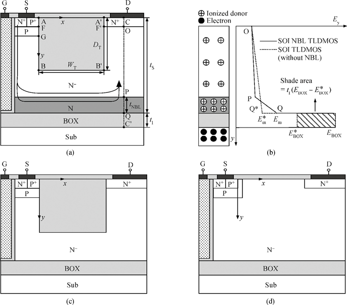
Fig. 1.
Schematic cross sections of (a) the proposed SOI NBL TLDMOS, (b) the charges distribution and the E-field profiles along the CC' line, (c) SOI TLDMOS, and (d) SOI TG LDMOS.
SEMICONDUCTOR DEVICES
Ye Fan, Xiaorong Luo, Kun Zhou, Yuanhang Fan, Yongheng Jiang, Qi Wang, Pei Wang, Yinchun Luo and Bo Zhang
Corresponding author: Luo Xiaorong, Email: xrluo@uestc.edu.cn
Abstract: A low specific on-resistance (Ron, sp) SOI NBL TLDMOS (silicon-on-insulator trench LDMOS with an N buried layer) is proposed. It has three features:a thin N buried layer (NBL) on the interface of the SOI layer/buried oxide (BOX) layer, an oxide trench in the drift region, and a trench gate extended to the BOX layer. First, on the on-state, the electron accumulation layer forms beside the extended trench gate; the accumulation layer and the highly doping NBL constitute an L-shaped low-resistance conduction path, which sharply decreases the Ron, sp. Second, in the y-direction, the BOX's electric field (E-field) strength is increased to 154 V/μm from 48 V/μm of the SOI Trench Gate LDMOS (SOI TG LDMOS) owing to the high doping NBL. Third, the oxide trench increases the lateral E-field strength due to the lower permittivity of oxide than that of Si and strengthens the multiple-directional depletion effect. Fourth, the oxide trench folds the drift region along the y-direction and thus reduces the cell pitch. Therefore, the SOI NBL TLDMOS structure not only increases the breakdown voltage (BV), but also reduces the cell pitch and Ron, sp. Compared with the TG LDMOS, the NBL TLDMOS improves the BV by 105% at the same cell pitch of 6 μm, and decreases the Ron, sp by 80% at the same BV.
Key words: MOSFET, silicon-on-insulator, breakdown voltage, specific on-resistance
| [1] |
Colak S, Singer B, Stupp E. Lateral DMOS power transistor design. IEEE Electron Device Lett, 1980, 1(4):51 doi: 10.1109/EDL.1980.25226
|
| [2] |
Hossain Z, Imam M, Fulton J, et al. Double-RESURF 700 V n-channel LDMOS with best-in-class on-resistance. IEEE ISPSD, 2002:137 http://ieeexplore.ieee.org/xpl/abstractKeywords.jsp?reload=true&arnumber=1016190&pageNumber%3D33887%26rowsPerPage%3D100
|
| [3] |
Zhou M J, De Bruycker A, Van Calster A, et al. Breakdown walkout and its reduction in high-voltage pLDMOS transistors on thin epitaxial layer. Electron Lett, 1992, 28(16):1537 doi: 10.1049/el:19920976
|
| [4] |
Efland T, Mei P, Mosher D, et al. Self-aligned RESURF to LOCOS region LDMOS characterization shows excellent Rsp vs BV performance. IEEE ISPSD, 1996:147 http://ieeexplore.ieee.org/xpl/articleDetails.jsp?reload=true&arnumber=509468
|
| [5] |
Lei Tianfei, Luo Xiaorong, Ge Rui, et al. Ultra-low specific on-resistance SOI double-gate trench-type MOSFET. Journal of Semiconductors, 2011, 32(10):104004 doi: 10.1088/1674-4926/32/10/104004
|
| [6] |
Hu Xiarong, Zhang Bo, Luo Xiaorong, et al. Universal trench design method for a high-voltage SOI trench LDMOS. Journal of Semiconductors, 2012, 33(7):074006 doi: 10.1088/1674-4926/33/7/074006
|
| [7] |
Son W S, Sohn Y H, Choi S Y. RESURF LDMOSFET with a trench for SOI power integrated circuits. Microelectron J, 2004, 35(5):393 doi: 10.1016/j.mejo.2004.02.001
|
| [8] |
Nakagawa A, Kawaguchi Y. Improved 20 V lateral trench gate power MOSFETs with very low on-resistance of 7.8 mΩ·mm2. IEEE ISPSD, 2000:47 https://ar.scribd.com/document/342904311/PowerManagement-SamDavis
|
| [9] |
Luo X R, Li Z J, Zhang B, et al. Realization of high voltage (>> 700 V) in new soi devices with a compound buried layer. IEEE Electron Device Lett, 2008, 29(12):1395 doi: 10.1109/LED.2008.2007307
|
| [10] |
Chen M, Wang Y B. Overview of SOI technologies in China. IEEE International SOI Conference, 2009:1 http://ieeexplore.ieee.org/abstract/document/5318787
|
| [11] |
Hu S D, Zhang B, Li Z J, et al. A new structure and its analytical model for the vertical interface electric field of a partial-SOI high voltage device. Chin Phys B, 2010, 19(3):37303 doi: 10.1088/1674-1056/19/3/037303
|
| [12] |
Luo Xiaorong, Hu Gangyi, Zhou Kun, et al. High voltage SOI LDMOS with a compound buried layer. Journal of Semiconductors, 2012, 33(10):104003 doi: 10.1088/1674-4926/33/10/104003
|
| [13] |
Nakagawa A, Yasuhara N, Baba Y. Breakdown voltage enhancement for devices on thin silicon layer/silicon dioxide film. IEEE Trans Electron Devices, 1991, 38(7):1650 doi: 10.1109/16.85162
|
| [14] |
Luo X R, Wang Y G, Yao G L, et al. Partial SOI power LDMOS with a variable low-k dielectric buried layer and a buried p-layer. IEEE ICSICT, 2010:2061 http://cpb.iphy.ac.cn/EN/article/downloadArticleFile.do?attachType=PDF&id=25242
|
| [15] |
Yang X M, Zhang B, Luo X R. Double enhance dielectric layer electric field high voltage SOI LDMOS. IEEE EDSSC, 2011:1 http://ieeexplore.ieee.org/xpls/abs_all.jsp?arnumber=6117731
|
| [16] |
Yan T, Liao H, Xiong Y, et al. Cost-effective integrated RF power transistor in 0.18-μm CMOS technology. IEEE Electron Device Lett, 2006, 27(10):856 doi: 10.1109/LED.2006.882568
|
| [17] |
Yasuhara N, Nakagawa A, Furukawa K. SOI device structures implementing 650 V high voltage output devices on VLSIs. Electron Devices Meeting, 1991:141 http://ieeexplore.ieee.org/xpls/abs_all.jsp?arnumber=235481
|
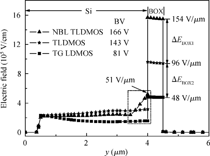
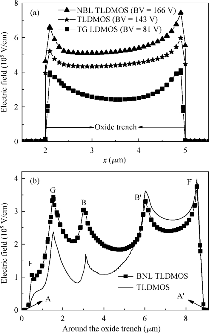
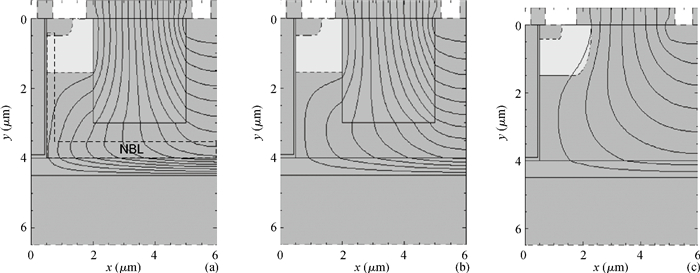
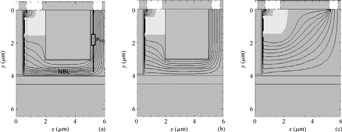
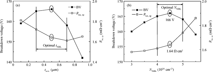
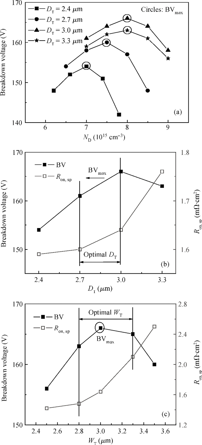

Table 1. Optimized NNBL, ND, BV and Ron; sp for SOI NBL TLDMOS, TLDMOS and TG LDMOS.

|
| [1] |
Colak S, Singer B, Stupp E. Lateral DMOS power transistor design. IEEE Electron Device Lett, 1980, 1(4):51 doi: 10.1109/EDL.1980.25226
|
| [2] |
Hossain Z, Imam M, Fulton J, et al. Double-RESURF 700 V n-channel LDMOS with best-in-class on-resistance. IEEE ISPSD, 2002:137 http://ieeexplore.ieee.org/xpl/abstractKeywords.jsp?reload=true&arnumber=1016190&pageNumber%3D33887%26rowsPerPage%3D100
|
| [3] |
Zhou M J, De Bruycker A, Van Calster A, et al. Breakdown walkout and its reduction in high-voltage pLDMOS transistors on thin epitaxial layer. Electron Lett, 1992, 28(16):1537 doi: 10.1049/el:19920976
|
| [4] |
Efland T, Mei P, Mosher D, et al. Self-aligned RESURF to LOCOS region LDMOS characterization shows excellent Rsp vs BV performance. IEEE ISPSD, 1996:147 http://ieeexplore.ieee.org/xpl/articleDetails.jsp?reload=true&arnumber=509468
|
| [5] |
Lei Tianfei, Luo Xiaorong, Ge Rui, et al. Ultra-low specific on-resistance SOI double-gate trench-type MOSFET. Journal of Semiconductors, 2011, 32(10):104004 doi: 10.1088/1674-4926/32/10/104004
|
| [6] |
Hu Xiarong, Zhang Bo, Luo Xiaorong, et al. Universal trench design method for a high-voltage SOI trench LDMOS. Journal of Semiconductors, 2012, 33(7):074006 doi: 10.1088/1674-4926/33/7/074006
|
| [7] |
Son W S, Sohn Y H, Choi S Y. RESURF LDMOSFET with a trench for SOI power integrated circuits. Microelectron J, 2004, 35(5):393 doi: 10.1016/j.mejo.2004.02.001
|
| [8] |
Nakagawa A, Kawaguchi Y. Improved 20 V lateral trench gate power MOSFETs with very low on-resistance of 7.8 mΩ·mm2. IEEE ISPSD, 2000:47 https://ar.scribd.com/document/342904311/PowerManagement-SamDavis
|
| [9] |
Luo X R, Li Z J, Zhang B, et al. Realization of high voltage (>> 700 V) in new soi devices with a compound buried layer. IEEE Electron Device Lett, 2008, 29(12):1395 doi: 10.1109/LED.2008.2007307
|
| [10] |
Chen M, Wang Y B. Overview of SOI technologies in China. IEEE International SOI Conference, 2009:1 http://ieeexplore.ieee.org/abstract/document/5318787
|
| [11] |
Hu S D, Zhang B, Li Z J, et al. A new structure and its analytical model for the vertical interface electric field of a partial-SOI high voltage device. Chin Phys B, 2010, 19(3):37303 doi: 10.1088/1674-1056/19/3/037303
|
| [12] |
Luo Xiaorong, Hu Gangyi, Zhou Kun, et al. High voltage SOI LDMOS with a compound buried layer. Journal of Semiconductors, 2012, 33(10):104003 doi: 10.1088/1674-4926/33/10/104003
|
| [13] |
Nakagawa A, Yasuhara N, Baba Y. Breakdown voltage enhancement for devices on thin silicon layer/silicon dioxide film. IEEE Trans Electron Devices, 1991, 38(7):1650 doi: 10.1109/16.85162
|
| [14] |
Luo X R, Wang Y G, Yao G L, et al. Partial SOI power LDMOS with a variable low-k dielectric buried layer and a buried p-layer. IEEE ICSICT, 2010:2061 http://cpb.iphy.ac.cn/EN/article/downloadArticleFile.do?attachType=PDF&id=25242
|
| [15] |
Yang X M, Zhang B, Luo X R. Double enhance dielectric layer electric field high voltage SOI LDMOS. IEEE EDSSC, 2011:1 http://ieeexplore.ieee.org/xpls/abs_all.jsp?arnumber=6117731
|
| [16] |
Yan T, Liao H, Xiong Y, et al. Cost-effective integrated RF power transistor in 0.18-μm CMOS technology. IEEE Electron Device Lett, 2006, 27(10):856 doi: 10.1109/LED.2006.882568
|
| [17] |
Yasuhara N, Nakagawa A, Furukawa K. SOI device structures implementing 650 V high voltage output devices on VLSIs. Electron Devices Meeting, 1991:141 http://ieeexplore.ieee.org/xpls/abs_all.jsp?arnumber=235481
|


Article views: 3192 Times PDF downloads: 21 Times Cited by: 0 Times
Received: 01 August 2013 Revised: 12 September 2013 Online: Published: 01 March 2014
| Citation: |
Ye Fan, Xiaorong Luo, Kun Zhou, Yuanhang Fan, Yongheng Jiang, Qi Wang, Pei Wang, Yinchun Luo, Bo Zhang. An L-shaped low on-resistance current path SOI LDMOS with dielectric field enhancement[J]. Journal of Semiconductors, 2014, 35(3): 034011. doi: 10.1088/1674-4926/35/3/034011
****
Y Fan, X R Luo, K Zhou, Y H Fan, Y H Jiang, Q Wang, P Wang, Y C Luo, B Zhang. An L-shaped low on-resistance current path SOI LDMOS with dielectric field enhancement[J]. J. Semicond., 2014, 35(3): 034011. doi: 10.1088/1674-4926/35/3/034011.

|
| [1] |
Colak S, Singer B, Stupp E. Lateral DMOS power transistor design. IEEE Electron Device Lett, 1980, 1(4):51 doi: 10.1109/EDL.1980.25226
|
| [2] |
Hossain Z, Imam M, Fulton J, et al. Double-RESURF 700 V n-channel LDMOS with best-in-class on-resistance. IEEE ISPSD, 2002:137 http://ieeexplore.ieee.org/xpl/abstractKeywords.jsp?reload=true&arnumber=1016190&pageNumber%3D33887%26rowsPerPage%3D100
|
| [3] |
Zhou M J, De Bruycker A, Van Calster A, et al. Breakdown walkout and its reduction in high-voltage pLDMOS transistors on thin epitaxial layer. Electron Lett, 1992, 28(16):1537 doi: 10.1049/el:19920976
|
| [4] |
Efland T, Mei P, Mosher D, et al. Self-aligned RESURF to LOCOS region LDMOS characterization shows excellent Rsp vs BV performance. IEEE ISPSD, 1996:147 http://ieeexplore.ieee.org/xpl/articleDetails.jsp?reload=true&arnumber=509468
|
| [5] |
Lei Tianfei, Luo Xiaorong, Ge Rui, et al. Ultra-low specific on-resistance SOI double-gate trench-type MOSFET. Journal of Semiconductors, 2011, 32(10):104004 doi: 10.1088/1674-4926/32/10/104004
|
| [6] |
Hu Xiarong, Zhang Bo, Luo Xiaorong, et al. Universal trench design method for a high-voltage SOI trench LDMOS. Journal of Semiconductors, 2012, 33(7):074006 doi: 10.1088/1674-4926/33/7/074006
|
| [7] |
Son W S, Sohn Y H, Choi S Y. RESURF LDMOSFET with a trench for SOI power integrated circuits. Microelectron J, 2004, 35(5):393 doi: 10.1016/j.mejo.2004.02.001
|
| [8] |
Nakagawa A, Kawaguchi Y. Improved 20 V lateral trench gate power MOSFETs with very low on-resistance of 7.8 mΩ·mm2. IEEE ISPSD, 2000:47 https://ar.scribd.com/document/342904311/PowerManagement-SamDavis
|
| [9] |
Luo X R, Li Z J, Zhang B, et al. Realization of high voltage (>> 700 V) in new soi devices with a compound buried layer. IEEE Electron Device Lett, 2008, 29(12):1395 doi: 10.1109/LED.2008.2007307
|
| [10] |
Chen M, Wang Y B. Overview of SOI technologies in China. IEEE International SOI Conference, 2009:1 http://ieeexplore.ieee.org/abstract/document/5318787
|
| [11] |
Hu S D, Zhang B, Li Z J, et al. A new structure and its analytical model for the vertical interface electric field of a partial-SOI high voltage device. Chin Phys B, 2010, 19(3):37303 doi: 10.1088/1674-1056/19/3/037303
|
| [12] |
Luo Xiaorong, Hu Gangyi, Zhou Kun, et al. High voltage SOI LDMOS with a compound buried layer. Journal of Semiconductors, 2012, 33(10):104003 doi: 10.1088/1674-4926/33/10/104003
|
| [13] |
Nakagawa A, Yasuhara N, Baba Y. Breakdown voltage enhancement for devices on thin silicon layer/silicon dioxide film. IEEE Trans Electron Devices, 1991, 38(7):1650 doi: 10.1109/16.85162
|
| [14] |
Luo X R, Wang Y G, Yao G L, et al. Partial SOI power LDMOS with a variable low-k dielectric buried layer and a buried p-layer. IEEE ICSICT, 2010:2061 http://cpb.iphy.ac.cn/EN/article/downloadArticleFile.do?attachType=PDF&id=25242
|
| [15] |
Yang X M, Zhang B, Luo X R. Double enhance dielectric layer electric field high voltage SOI LDMOS. IEEE EDSSC, 2011:1 http://ieeexplore.ieee.org/xpls/abs_all.jsp?arnumber=6117731
|
| [16] |
Yan T, Liao H, Xiong Y, et al. Cost-effective integrated RF power transistor in 0.18-μm CMOS technology. IEEE Electron Device Lett, 2006, 27(10):856 doi: 10.1109/LED.2006.882568
|
| [17] |
Yasuhara N, Nakagawa A, Furukawa K. SOI device structures implementing 650 V high voltage output devices on VLSIs. Electron Devices Meeting, 1991:141 http://ieeexplore.ieee.org/xpls/abs_all.jsp?arnumber=235481
|

 WeChat ID
Journal of Semiconductors © 2017 All Rights Reserved 京ICP备05085259号-2

 DownLoad:

