Processing math: 100%
J. Semicond. > 2024, Volume 45 > Issue 10 > 102101

ARTICLES

Impact of strain relaxation on the growth rate of heteroepitaxial germanium tin binary alloy

Pedram Jahandar and Maksym Myronov

+ Author Affiliations

 Corresponding author: Pedram Jahandar, P.Jahandar@warwick.ac.uk

DOI: 10.1088/1674-4926/24030002CSTR: 32376.14.1674-4926.24030002

PDF

Turn off MathJax

Abstract: 
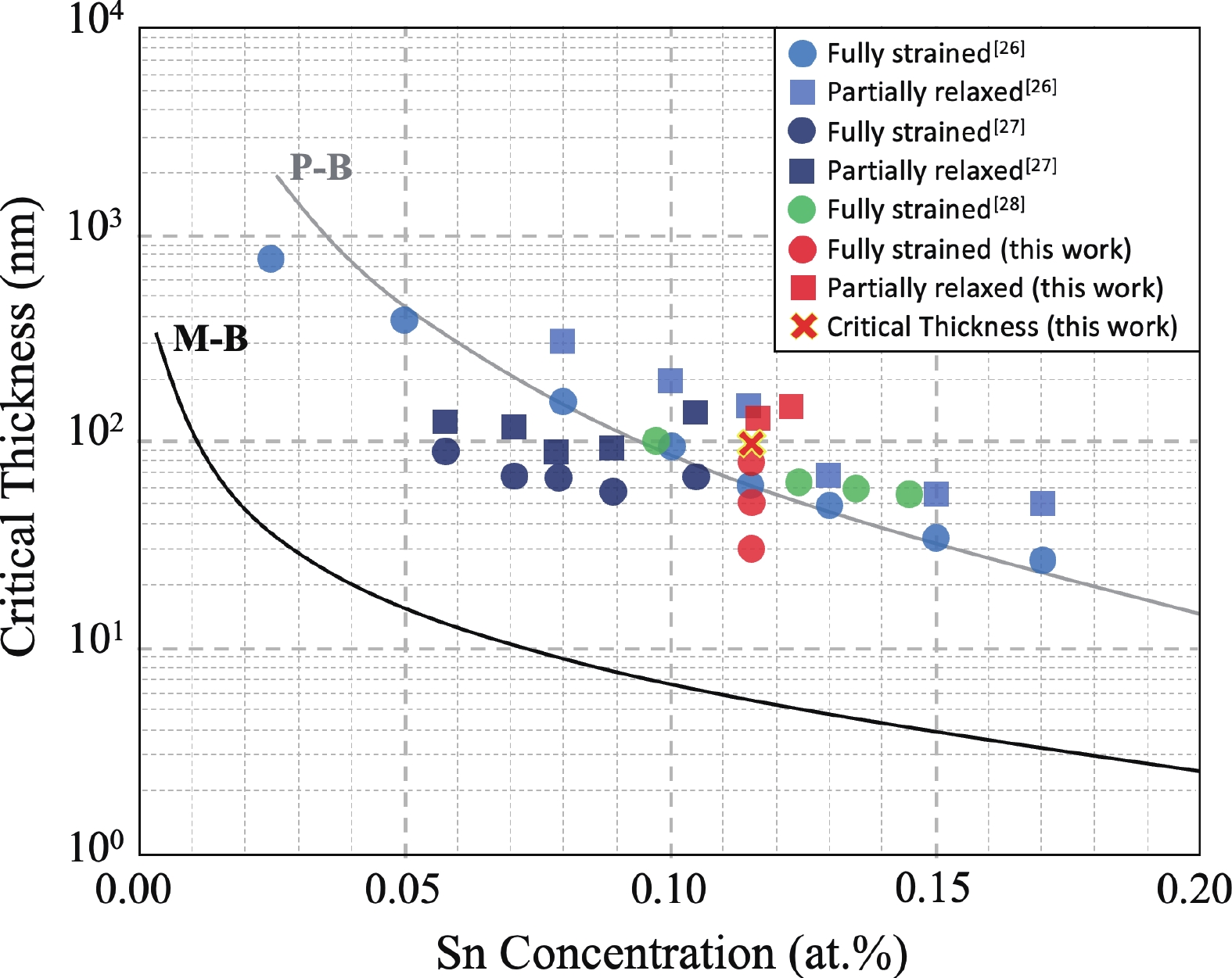
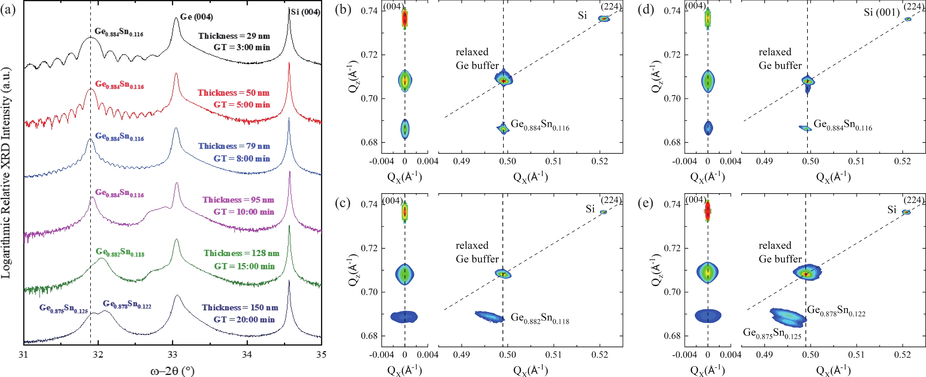
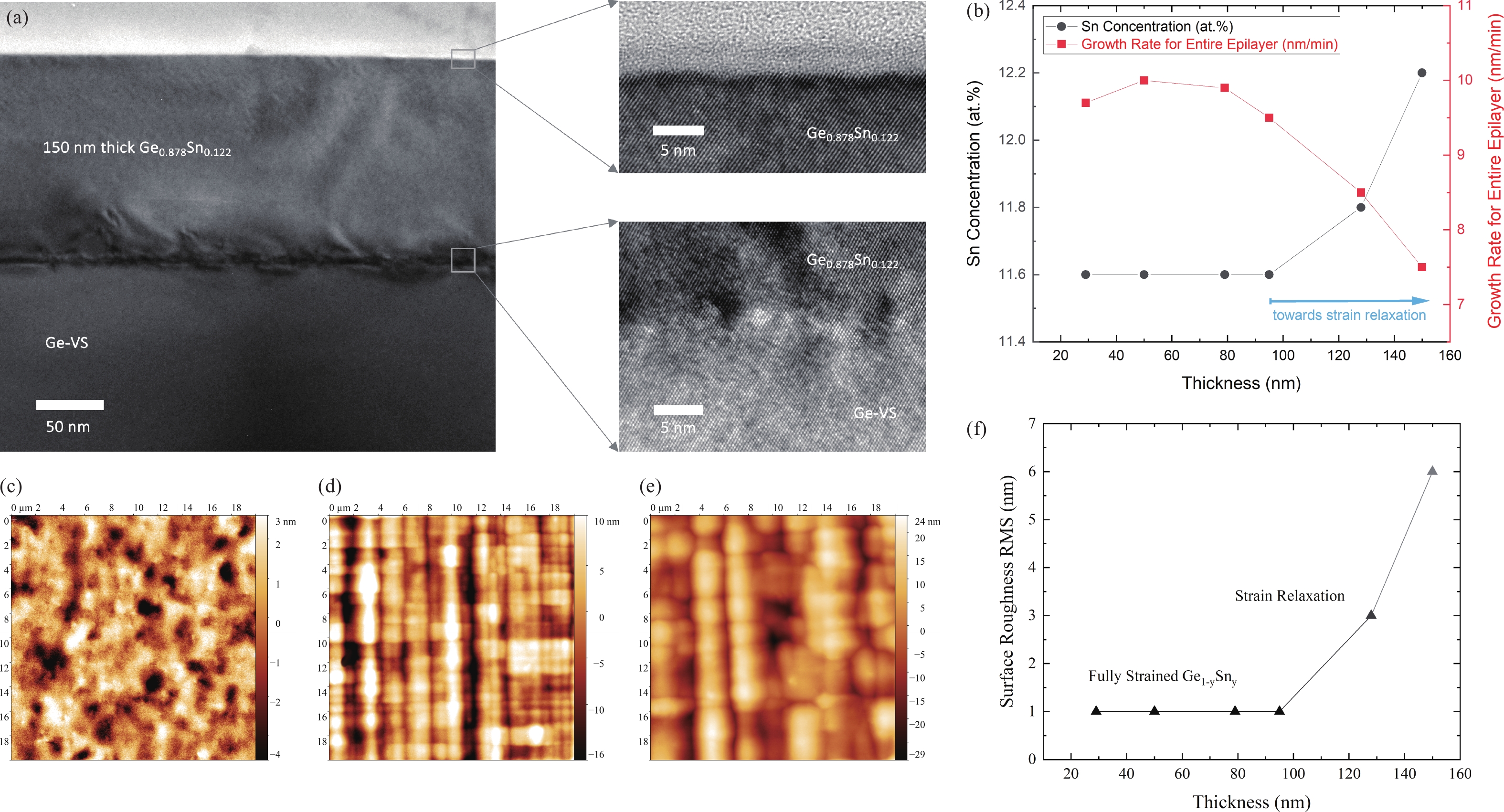
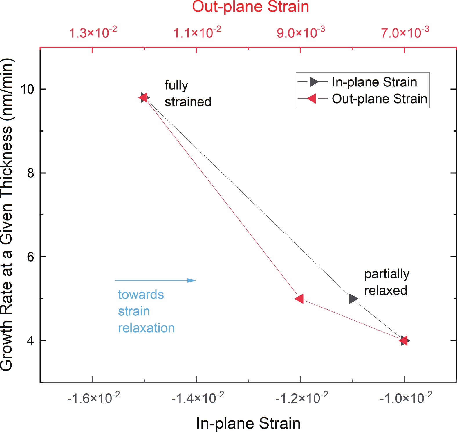
The growth of high-quality germanium tin (Ge1–ySny) binary alloys on a Si substrate using chemical vapor deposition (CVD) techniques holds immense potential for advancing electronics and optoelectronics applications, including the development of efficient and low-cost mid-infrared detectors and light sources. However, achieving precise control over the Sn concentration and strain relaxation of the Ge1–ySny epilayer, which directly influence its optical and electrical properties, remain a significant challenge. In this research, the effect of strain relaxation on the growth rate of Ge1–ySny epilayers, with Sn concentration >11at.%, is investigated. It is successfully demonstrated that the growth rate slows down by ~55% due to strain relaxation after passing its critical thickness, which suggests a reduction in the incorporation of Ge into Ge1–ySny growing layers. Despite the increase in Sn concentration as a result of the decrease in the growth rate, it has been found that the Sn incorporation rate into Ge1–ySny growing layers has also decreased due to strain relaxation. Such valuable insights could offer a foundation for the development of innovative growth techniques aimed at achieving high-quality Ge1–ySny epilayers with tuned Sn concentration and strain relaxation.

Key words: GeSngermanium tinstrain relaxationgroup Ⅳ semiconductorchemical vapour depositionCVD

The fundamental electronic energy bandgap is the most important parameter of a semiconductor, upon which other electronic and optical properties sensitively depend. It is crucial to carefully control the bandgap to optimise the performance of semiconductor devices. Bandgap engineering can be achieved by changing compositions in a semiconductor alloy system[1]. The field of bandgap engineering was significantly expanded with the introduction of epitaxial growth techniques[2]. Epitaxy refers to growth of crystalline layer, known as epitaxial layer, on top of a crystalline substrate with the same orientation. In this technique, large stresses in epitaxial layers are generated because of lattice constant mismatch between epitaxial layer and substrate[3]. The strain in epitaxial layer provides an additional design flexibility for electronic band structure engineering. However, such flexibility is influenced and limited to a critical thickness of epitaxial layer, where strain starts to relieve due to formed defects as a consequence of strain relaxation[3]. For example, if lattice constant of epitaxial layer significantly depends on its composition, appropriate composition could lead to significant strain energy and so large reduction in hc into an undesirable value. When growing a material with the same crystal structure with a different lattice constant from the substrate or buffer layer (referred to as a virtual substrate (VS)), the grown material either has a tensile strain or a compressive strain. In the case of Ge1–ySny grown on Ge-VS (or Si substrate), the grown Ge1–ySny epilayer will have a compressive strain because its lattice constant is larger than that of Ge-VS (or Si substrate). If the grown Ge1–ySny has exactly the same inner plane (in-plane) lattice parameter as its Ge-VS (or Si substrate) but a larger outer plane (out-of-plane) lattice parameter, it is referred to as a fully strained Ge1–ySny. Fully strained Ge1–ySny epilayer can be grown up to a certain thickness, so called critical thickness hc, which mainly depends on Sn concentration (y). Above hc, Ge1–ySny epilayer gradually begins to relax the compressive strain.

The lattice constant of Ge1–ySny is larger than that of Ge; however, this lattice constant closely depends on the Sn concentration in Ge1–ySny, especially in samples that are not fully strained. As the Sn concentration (y) in the Ge1–ySny binary alloy increases, its lattice volume is expected to increase. The growth of high quality Ge1–ySny, in which segregation and precipitation is controlled, directly on Si substrate using CVD is very challenging due to its large lattice mismatch. To overcome this challenge, a high quality relaxed Ge buffer, which has a larger lattice constant than Si, can be grown on Si substrate and used as an intermediate layer, VS, to reduce the effective lattice mismatch. The strain is a key parameter that influences the physical, optical, and electrical properties of the Ge1–ySny epilayer. For example, it has been suggested that tensile and compressive strain reduce and increase the required Sn concentration to achieve indirect-to-direct bandgap transition, respectively[4, 5]. In addition to Sn concentration, it is possible to adjust carrier mobility[6, 7] and band structure[4, 8] of the epilayer by modifying the strain in the Ge1–ySny epilayer. Therefore, it is essential to fully understand the strain relaxation of Ge1–ySny epilayers.

Theoretically, it should be possible to tune the room temperature energy bandgap of Ge1–ySny alloy from 0.66 eV down to 0.0 eV by modifying the Sn concentration in Ge1–ySny[9, 10]. Ge is a group Ⅳ semiconductor with an indirect bandgap and an energy difference of 0.66 eV between the lowest conduction band minimum, L-point, and the highest valence band maximum, Γ-point, at room temperature[5]. As y increases in Ge1–ySny, the L-valleys diminishes slower than the Γ-valley as a consequence of EgΓ,GeEgΓ,αSn ˃ EgL,GeEgL,αSn, suggesting an indirect-to-direct bandgap transition for a certain[5]. It has been shown that bandgap energy decreases as a result of tensile biaxial strain in Ge1–ySny, as the effect of strain is significantly higher in direct gap than indirect[11, 12]. The achievement of direct bandgap Ge1–ySny depends strongly on its strain relaxation, for instance, for compressive strained Ge1–ySny, higher Sn concentration is required for an indirect-to-direct bandgap transition than tensile strained Ge1–ySny[5].

Theoretical investigations have shown that biaxial strain can significantly affect the bandgap structure of Ge1–ySny. Specifically, it has been suggested that tensile and compressive strains can respectively decrease and increase the required Sn concentration to achieve an indirect-to-direct bandgap transition in Ge1–ySny[4]. Tensile strained Ge1–ySny can be grown on partially or fully relaxed Ge1–ySny with a different Sn concentration[1720], while compressive strained Ge1–ySny can be grown on Si via Ge-VS[21, 22]. Recent predictions indicate that an indirect-to-direct bandgap transition in Ge1–ySny can be achieved with a Sn concentration ranging from 6 at.% to 11 at.%[4, 2327].

Therefore, it is crucial to have a comprehensive understanding of the impact of strain relaxation on the growth rate of Ge1–ySny epilayers, in addition to understanding its critical thickness and Sn concentration, to facilitate the development of optoelectronic devices. As seen in Fig. 1, many studies have been carried out to estimate critical thicknesses and the effect of strain relaxation on Sn concentration as well as quality of epilayers. However, no study has been done to investigate the effect of strain relaxation on growth rate, which is presented in this research.

Fig. 1.  (Colour online) Theoretical calculations of hc for Ge1–ySny films grown on Si substrate via a relaxed Ge-VS using the People Bean (P–B) model and the Matthew Blakeslee (M–B) model[13]. Experimental data collected from this work as well as previous research are included[1416].

In this research, all crystalline materials were grown using the ASM Epsilon 2000 system. It is one of the most common epitaxy tools in semiconductor manufacturing, having been used for about three decades to grow Si, Ge, Si1–xGex, Si1–xCx and many other group Ⅳ semiconductors. It is a horizontal flow, load-locked, and single wafer reduced-pressure chemical vapour deposition (RP-CVD) tool developed for high-volume semiconductor production in various epitaxy applications. The Si wafer is mounted on a graphite susceptor coated with silicon carbide, which is located in a quartz chamber with a cold wall. During the process, infrared (IR) lamps are responsible for heating the susceptor and the wafer, ones placed on the bottom and the others on the top of the quartz chamber. To control growth at low temperatures, thermocouples embedded in the susceptor are used.

All Ge1–ySny epilayers were grown on 100 mm Si (001) wafers via 0.6 µm thick relaxed Ge virtual substrate. By growing thick enough Ge buffer layer on top of Si (001), strain relaxation within the Ge buffer layer is achieved and so effective lattice mismatch between Si substrate and Ge1–ySny decreases from ~20 % to ~15 %[5]. Tin-tetrachloride (SnCl4) was used in combination with germane (GeH4) with H2 as a carrier gas and chamber pressure controller. All growth was carried out at 260 °C and 500 Torr.

The Sn concentration of each Ge1–ySny epilayer was measured using high-resolution X-ray diffraction (HR-XRD). HR-XRD ω–2θ coupled scan, symmetric and asymmetric reciprocal space maps (RSMs) were used, alongside with the modified Vegard’s law to measure the Sn concentrations. The Vegard’s law used in this research is:

aGe1ySny0=(1y)aGe0+yaSn0+y(1y)bGeSn, (1)

where a0 is the relaxed lattice constant of each crystal, and bGeSn is the bowing parameter. The bowing parameter (bGeSn) used in this research is 0.041 Å[15] according to the latest agreed studies and relaxed lattice constant, a0 is 5.6579 and 6.4892 Å for Ge and Sn, respectively[5]. The lattice constant of each epilayer was calculated from the in and out of plane lattice parameters obtained from RSMs.

In this work, the hc value of Ge1–ySny, which represents the thickness where strain relaxation begins in the epilayer, is initially investigated. The Sn concentration of 11.6 at.% was obtained for the fully strained Ge1–ySny epilayers. The Sn concentration for each sample was measured from RSMs using the modified Vegard’s law. As seen in Fig. 2(a), the thickness fringes around Ge1–ySny peak in HR-XRD ω–2θ coupled scan for the Ge1–ySny epilayer grown for 10 min began to disappear. This indicates the beginning of strain relaxation in the Ge1–ySny epilayer. The thickness of the Ge1–ySny epilayer grown for 10 min was measured using X-TEM to be 95 nm. This shows that the hc value for Ge1–ySny epilayers grown under the given CVD growth conditions is approximately ~95 nm which agrees with previous studies shown in Fig. 1.

Fig. 2.  (Colour online) (a) HR-XRD ω–2θ coupled scans for Ge1–ySny epilayers grown with different growth times on Si (001) via Ge-VS. Symmetric and asymmetric RSMs for Ge1–ySny grown with different growth times on Si (001) via Ge-VS of (b) 79 nm thick Ge0.884Sn0.116 grown for 8 min, (c) 95 nm thick Ge0.884Sn0.116 grown for 10 min, (d) 128 nm thick Ge0.882Sn0.118 grown for 15 min, and (e) 150 nm thick Ge0.878Sn0.122 grown for 20 min. The Sn concentration for each of these samples was measured from RSMs and using the modified Vegard’s law. The thicknesses of these epilayers are measured using either thickness fringes appeared in their HR-XRD ω–2θ coupled scans or X-TEM images, as shown in the example in Fig. 3(a).

When comparing the HR-XRD ω–2θ coupled scans of the Ge1–ySny epilayers shown in Fig. 2(a), it becomes evident that as more strain relaxation is achieved, the Ge1–ySny peak in the HR-XRD ω–2θ coupled scan begins to shift to the right. This shift is solely due to strain relaxation within the layers of Ge1–ySny and not to a reduction in Sn concentration. This is demonstrated when measuring the Sn concentration using XRD RSMs.

As shown in Fig. 2(b), the Ge1–ySny grown for 8 min is fully strained, and its peak appeared exactly under the relaxed Ge-VS in the asymmetric RSM. However, for the Ge1–ySny grown for 10 min, as shown in Fig. 2(c), the Ge1–ySny peak in the asymmetric RSM is slightly shifted to the left, indicating the appearance of strain relaxation in the Ge1–ySny layers. In addition, for the Ge1–ySny grown for 15 min, as shown in Fig. 2(d), the Ge1–ySny peak in the asymmetric RSM is significantly shifted to the left, indicating a greater degree of strain relaxation in the Ge1–ySny layers compared to the previous epilayer, which was grown for only 10 min. As shown in Fig. 2(d), the Sn concentration of the Ge1–ySny epilayer grown under the same CVD growth conditions has indeed increased due to strain relaxation. The Ge1–ySny epilayer grown for 15 min has 0.2 at.% more Sn concentration than the fully strained Ge1–ySny epilayer grown for 8 min. For the Ge1–ySny epilayer grown for 10 min, no change in Sn concentration was observed as the epilayer has just begun to relax at the hc of ~95 nm.

An additional Ge1–ySny epilayer was also grown for 15 min under the same growth conditions, indicating a relaxation of strain in the epilayer. The thickness of this epilayer is also measured using X-TEM. As seen in Fig. 2(a), an additional peak is observed next to each of the HR-XRD ω–2θ coupled scans of Ge1–ySny epilayers (with apparent strain relaxation), which were grown for 10 and 15 min. It should be noted that shoulders on the left side of the Ge peak in HR-XRD ω–2θ coupled scans are normally considered to be due to polycrystalline Ge1–ySny or Ge1–ySny with very low Sn concentration (around Sn solubility in Ge). Nevertheless, as can be seen in Fig. 2(a), such peaks or shoulders are not present in HR-XRD ω–2θ coupled scans of fully strained Ge1–ySny epilayers grown under the same CVD conditions. The apparent shoulders are presumably due to Sn segregation, especially considering they are not evident for fully strained Ge1–ySny epilayers. As such, the shoulder does not appear in the HR-XRD ω–2θ coupled scan of the 150 nm thick Ge0.878Sn0.122. It may depend on the area of the epilayer scanned; thus, some areas on the wafers have no Sn segregation.

A thicker Ge1–ySny epilayer was grown for 20 min under the same growth conditions. Symmetric and asymmetric RSMs of the heterostructure are shown in Fig. 2(e). At first glance, two Ge1–ySny peaks in the asymmetric RSM can be noticed. Before discussing the double Ge1–ySny peaks, it is important to note that both Ge1–ySny peaks are more relaxed (shifted more to the left in asymmetric RSM) than the Ge1–ySny peak in asymmetric RSM of thinner Ge1–ySny epilayers. In addition, both Ge1–ySny peaks indicate higher Sn concentrations than thinner Ge1–ySny, as shown in Fig. 2, confirming an increase in Sn concentration due to strain relaxation. In Fig. 3(a), high resolution X-TEM of Ge0.878Sn0.122 is given which shows thickness and smooth surface of the epilayer.

Fig. 3.  (Colour online) (a) X-TEM image of 150 nm thick Ge0.878Sn0.122 grown on Ge-VS. The high resolution lattice resolved X-TEM micrographs of Ge0.878Sn0.122/Ge-VS interface as well as surface of Ge0.878Sn0.122 epilayer are presented. (b) Relationship between thickness, Sn concentration and total growth rate of Ge1–ySny epilayers. (c) AFM scan of 95 nm thick Ge0.884Sn0.116. (d) AFM scan of 128 nm thick Ge0.882Sn0.118. (e) AFM scan of 150 nm thick Ge0.878Sn0.122. (f) Surface roughness (RMS) of Ge1–ySny epilayers with different thicknesses. Surface roughness increased with the increase in thickness (growth time), particularly after the critical thickness of ~95 nm.

A summary of the relationship between thickness, Sn concentration and total growth rate of Ge1–ySny epilayers is shown in Fig. 3(b). For the Ge1–ySny epilayer with growth time of 20 min (150 nm thick Ge1–ySny epilayer), only one peak is included (the one with lower Sn concentration). It should be noted that this summary is only valid for Ge1–ySny epilayers grown under the same CVD conditions using the same precursors and respective partial pressures. This is because each of these CVD conditions can influence lattice diffusion and thus hc. For example, as the growth temperature decreases, lattice diffusion is minimised which may increases the hc. Another example is the Sn concentration itself: as the Sn concentration in the Ge1–ySny epilayer increases, the hc decreases, so the epilayer strain relaxation is achieved more quickly.

Moreover, if the thickness of the Ge1–ySny epilayer is greater than hc, misfit dislocations can form at the two ends[28]. These dislocations could create a loop so that the two ends can join or thread onto the surface, which could potentially restrict applications of relaxed Ge1–ySny[6, 29]. Examples of AFM scans of the epilayers with various thicknesses are provided in Figs. 3(c)–3(e). The surface roughness in terms of RMS for all Ge1–ySny epilayers grown in this study is shown in Fig. 3(f). It is evident that the surface roughness remained low for all fully strained Ge1–ySny, and as soon as a hc of ~95 nm was reached (at growth time of ~10 min), the surface roughness began to increase. This could be due to Sn segregation, which may be a consequence of strain relaxation[30].

It is important to discuss the reasons for the appearance of two Ge1–ySny peaks (as can be seen in Fig. 2(e)) in asymmetric RSM of Ge1–ySny epilayer grown for 20 min. The justification for this behaviour is as follows: the second peak, which indicates that Ge1–ySny layers with a slightly higher Sn concentration can be grown when a certain strain relaxation is achieved. The Sn concentration increases gradually and steadily as the layers relax (as the thickness of the epilayer increases) until a certain point. After this certain point, there is a sudden transition to Sn concentration, because the top layers (which now act as an intermediate substrate) allow Ge1–ySny to grow with such a higher Sn concentration.

In this section, the effect of strain relaxation on the growth rate of Ge1–ySny epilayers is investigated. As shown in Fig. 3(b), the growth rate of Ge1–ySny epilayers decreases with increasing thickness. The growth rates shown in Fig. 3(b) are the growth rates for the entire Ge1–ySny epilayers. To understand the effect of strain relaxation on growth rate, it is therefore necessary to investigate the relationship between growth rate and thickness of Ge1–ySny epilayers.

As shown in Fig. 4(a), the average growth rate for fully strain Ge1–ySny grown up to 10 min under the given CVD conditions was 9.8 nm/min. We assumed that for partially relaxed Ge1–ySny epilayers, which were grown for 15 and 20 min, the growth rate for the initial 10 min was the same as the growth rate for fully strained Ge1–ySny epilayers. Based on this assumption, the average growth rate from 10 to 15 min was measured at 6.1 nm/min and the average growth rate from 15 to 20 min was measured at 4.4 nm/min. These growth rates were calculated by growing Ge1–ySny with different growth times.

Fig. 4.  (Colour online) (a) Average growth rate (nm/min) at the given thickness (nm) of the Ge1–ySny and its corresponding growth time (min). As the thickness of the Ge1–ySny increases, the growth rate decreases. (b) Actual data points collected experimentally for average growth rate (nm/min).

Considering the average growth rates of the epilayers depending on their thickness as shown in Fig. 4(a), it is possible to understand the effect of strain relaxation on growth rates. As shown in Fig. 4(b), a straight line (orange colour) is fitted to the data, representing the average growth rate at the given thickness of the Ge1–ySny epilayer. For thicknesses below the hc, in which all Ge1–ySny epilayers are fully strained, the growth rate is assumed to remain constant. Therefore, a straight horizontal line was fitted to those epilayers with thickness of up to hc. The epilayers with thickness of above hc are partially relaxed and their degree of relaxation is discussed in the next Section. It is also evident that the rate of suppression in the average growth rate is at its highest level just after the Ge1–ySny epilayer passes the hc, and the rate of reduction in the average growth rate gradually decreases as the thickness of the epilayer increases.

The in-plane and out-of-plane strain of Ge1–ySny epilayers grown were estimated using the following equations:

Straininplane=aGeSnaGeSn0aGeSn0, (2)
Strainoutofplane=aGeSnaGeSn0aGeSn0, (3)

where a and a are in-plane and out-of-plane of the lattice respectively. Additionally, aGeSn0 refers to the relaxed lattice constant for Ge1–ySny at a given Sn concentration, and GeSn refers to the actual Ge1–ySny epilayer grown and its HR-XRD ω–2θ coupled scan and RSMs were collected.

In-plane and out-of-plane strain of grown Ge1–ySny epilayers were calculated using Eqs. (1) and (2) and presented in Table 1. It is evident that the thickness of the Ge1–ySny epilayer does not affect the in-plane or out-of-plane strain if the thickness is less than the hc (~0.10 µm). However, when the thickness of the Ge1–ySny epilayer exceeds hc, the strain relaxation begins, and both the in-plane and out-of-plane strains of the epilayer converge towards relaxed lattice constant, aGeSn0.

Table 1.  Summary of effects of strain relaxation on the Sn concentration and growth rate of Ge1–ySny epilayers grown at 260 °C and 500 Torr on Si (001) via a relaxed Ge-VS.
Thickness (nm) In-plane strain
(10–3)
Out-of-plane strain (10–3) Average Sn content (at.%) Average growth rate (nm/min)
29 –15.4 12.1 11.6 9.7
50 –15.6 12.2 11.6 10.0
79 –15.8 12.4 11.6 9.9
95 –15.6 12.3 11.6 9.5
128 –11.1 8.7 11.8 8.5
150 –9.8 7.7 12.2 7.5
–9.3 7.3 12.5
DownLoad: CSV  | Show Table

By considering the measured in-plane and out-of-plan strain, it is possible to investigate the effect of strain relaxation on both the growth rate and Sn concentration of Ge1–ySny epilayers. As shown in Table 1, the average growth rate decreases as more strain relaxation are achieved. These average growth rates represent the growth rate for the entire Ge1–ySny epilayers, not at a given in-plane or out-of-plane strain (or simply at a given thickness). To determine the true growth rate at a given thickness, the fitted line to the actual data shown in Fig. 4(b) can be used. Using this approach, the growth rate at a thickness of 128 nm was estimated to be ~5 nm/min and at a thickness of 150 nm was estimated to be ~4 nm/min. Based on these estimates, the effect of strain relaxation on the growth rate at given thicknesses can be explored. As shown in Fig. 5, the growth rate at the given thickness of the Ge1–ySny epilayer is (almost) linearly dependent on the in-plane and out-of-plane strain. Since only two data points are available for partially relaxed Ge1–ySny, more studies are required to investigate further the effect of strain relaxation on the growth rate of the Ge1–ySny epilayer at a given thickness.

Fig. 5.  (Colour online) The effect of strain relaxation in Ge1–ySny epilayers on their growth rate. The growth rate at given strain relaxation state was estimated using the fitted line to the actual data points given in Fig. 4. In-plane and out-of-plane strain were calculated by Eqs. (1) and (2).

As explained previously, the growth rate of Ge1–ySny mainly depends on the Ge incorporation in the growing layers. Since all growth conditions such as temperature, pressure and partial pressures of precursors remained constant over the growth of all Ge1–ySny epilayers, the production of Ge and Sn atoms remained constant. Therefore, the suppression of the Ge incorporation in growing layers cannot be due to the lack of Ge adatoms produced in the chamber. It seems that the strain relaxation directly influences the incorporation of Ge. As Ge1–ySny relaxes more, a lower percentage of available Ge adatoms on the growing layers can be incorporated into the growing layers, resulting in a reduction in the growth rate.

Finally, the effect of strain relaxation on average Sn concentration can be examined. Here, we are discussing only the average Sn concentration across the entire Ge1–ySny epilayer, rather than the Sn concentration at a specific thickness of the Ge1–ySny epilayer. As shown in Table 1, the average Sn concentration increases as a result of strain relaxation. This can be explained by taking into account the effect of the growth rate on the average Sn concentration of Ge1–ySny epilayers. Like Ge production, as CVD growth conditions remained the same, the production of Sn adatoms remained the same during the growth of Ge1–ySny epilayer. Therefore, as the growth rate decreases, more of supplied Sn adatoms have the chance to incorporate into Ge1–ySny growing layers, leading to an increase in Sn concentration.

It should be noted that even though the average growth rate decreases by ~55 % due decrease in incorporation of Ge into growing layers as a result of strain relaxation, the average Sn concentration in Ge1–ySny has increased only by ~8 % from 11.6 at.% to 12.5 at.%. It is important to consider that this is the average Sn concentration of the whole epilayer and not just the top layers grown with lower growth rates. This result shows that the total Sn concentration does not significantly increase as a result of the reduction in growth rate, and the relationship could be nonlinear. This suggests that the incorporation rate of Sn into the growing Ge1–ySny layers during the total growth time has indeed decreased, and the reason why the total Sn concentration is increased is because of the reduction in growth rate itself.

In this research, the effect of strain relaxation in compressive strained Ge1–ySny, which were grown at 260 °C, on growth rate is investigated. It is experimentally shown that strain relaxation within Ge1–ySny decreases the growth rate of the epilayer. We also examined how Sn concentration and surface morphology of Ge1–ySny epilayers may be influenced as a result of strain relaxation. It is important to note that strain relaxation could be potentially different in Ge1–ySny epilayers with the same Sn concentration but grown under different CVD growth conditions. More experiments should be carried out to investigate strain relaxation for Ge1–ySny epilayers grown under different CVD growth conditions. Furthermore, since the strain relaxation in Ge1–ySny epilayers affects the electrical, for example indirect-to-direct bandgap transition[4, 2327], and the physical properties of epilayers, it is therefore essential to consider further investigations in order to fully understand the mechanism of strain relaxation of Ge1–ySny epilayers. This could pave the way for the widespread adoption of Ge1–ySny based semiconductor devices and applications in the near future.


[1]
Johnson E R, Christian S M. Some properties of germanium-silicon alloys. Phys Rev, 1954, 95, 560 doi: 10.1103/PhysRev.95.560
[2]
Göbel E O, Ploog K. Fabrication and optical properties of semiconductor quantum wells and superlattices. Prog Quantum Electron, 1990, 14, 289 doi: 10.1016/0079-6727(90)90001-E
[3]
Joyce B A. Materials fundamentals of molecular beam epitaxy. Adv Mater, 1993, 5, 773 doi: 10.1002/adma.19930051028
[4]
Gupta S, Magyari-Köpe B, Nishi Y, et al. Achieving direct band gap in germanium through integration of Sn alloying and external strain. J Appl Phys, 2013, 113, 73707 doi: 10.1063/1.4792649
[5]
Wirths S, Buca D, Mantl S. Si–Ge–Sn alloys: From growth to applications. Prog Cryst Growth Charact Mater, 2016, 62, 1 doi: 10.1016/j.pcrysgrow.2015.11.001
[6]
Lieten R R, Maeda T, Jevasuwan W, et al. Tensile-strained GeSn metal–oxide–semiconductor field-effect transistor devices on Si(111) using solid phase epitaxy. Appl Phys Express, 2013, 6, 101301 doi: 10.7567/APEX.6.101301
[7]
Guo P F, Han G Q, Gong X, et al. Ge0.97Sn0.03 p-channel metal-oxide-semiconductor field-effect transistors: Impact of Si surface passivation layer thickness and post metal annealing. J Appl Phys, 2013, 114, 044510 doi: 10.1063/1.4816695
[8]
Eckhardt C, Hummer K, Kresse G. Indirect-to-direct gap transition in strained and unstrained Sn xGe1– x alloys. Phys Rev B, 2014, 89, 165201 doi: 10.1103/PhysRevB.89.165201
[9]
Zheng J, Liu Z, Xue C L, et al. Recent progress in GeSn growth and GeSn-based photonic devices. J Semicond, 2018, 39, 061006 doi: 10.1088/1674-4926/39/6/061006
[10]
Oguz S, Paul W, Deutsch T F, et al. Synthesis of metastable, semiconducting Ge-Sn alloys by pulsed UV laser crystallization. Appl Phys Lett, 1983, 43, 848 doi: 10.1063/1.94524
[11]
Soref R A, Friedman L. Direct-gap Ge/GeSn/Si and GeSn/Ge/Si heterostructures. Superlattices Microstruct, 1993, 14, 189 doi: 10.1006/spmi.1993.1122
[12]
Gurdal O, Desjardins P, Carlsson J R A, et al. Low-temperature growth and critical epitaxial thicknesses of fully strained metastable Ge1– xSnx (x≤0.26) alloys on Ge(001)2 × 1. J Appl Phys, 1998, 83, 162 doi: 10.1063/1.366690
[13]
Mosleh A, Ghetmiri S A, Conley B R, et al. Material characterization of Ge1− xSn xAlloys grown by a commercial CVD system for optoelectronic device applications. J Electron Mater, 2014, 43, 938 doi: 10.1007/s11664-014-3089-2
[14]
Wang W, Zhou Q, Dong Y, et al. Critical thickness for strain relaxation of Ge1–i>xSnx (x ≤ 0.17) grown by molecular beam epitaxy on Ge(001). Appl Phys Lett, 2015, 106, 232106 doi: 10.1063/1.4922529
[15]
Gencarelli F, Vincent B, Demeulemeester J, et al. Crystalline properties and strain relaxation mechanism of CVD grown GeSn. ECS J Solid State Sci Technol, 2013, 2, P134 doi: 10.1149/2.011304jss
[16]
Bhargava N, Coppinger M, Prakash Gupta J, et al. Lattice constant and substitutional composition of GeSn alloys grown by molecular beam epitaxy. Appl Phys Lett, 2013, 103, 041908 doi: 10.1063/1.4816660
[17]
Takeuchi S, Sakai A, Yamamoto K, et al. Growth and structure evaluation of strain-relaxed Ge1– xSn x buffer layers grown on various types of substrates. Semicond Sci Technol, 2007, 22, S231 doi: 10.1088/0268-1242/22/1/S54
[18]
Takeuchi S, Shimura Y, Nakatsuka O, et al. Growth of highly strain-relaxed Ge1– xSnx/virtual Ge by a Sn precipitation controlled compositionally step-graded method. Appl Phys Lett, 2008, 92, 231916 doi: 10.1063/1.2945629
[19]
Takeuchi S, Sakai A, Nakatsuka O, et al. Tensile strained Ge layers on strain-relaxed Ge1–xSnx/virtual Ge substrates. Thin Solid Films, 2008, 517, 159 doi: 10.1016/j.tsf.2008.08.068
[20]
Wirths S, Tiedemann A T, Ikonic Z, et al. Band engineering and growth of tensile strained Ge/(Si)GeSn heterostructures for tunnel field effect transistors. Appl Phys Lett, 2013, 102, 192103 doi: 10.1063/1.4805034
[21]
Weisshaupt D, Jahandar P, Colston G, et al. Impact of Sn segregation on Ge1− xSnx epi-layers growth by RP-CVD. 2017 40th International Convention on Information and Communication Technology, Electronics and Microelectronics (MIPRO), 2017, 43 doi: 10.23919/MIPRO.2017.7973388
[22]
Jahandar P, Weisshaupt D, Colston G, et al. The effect of Ge precursor on the heteroepitaxy of Ge1– xSn x epilayers on a Si (001) substrate. Semicond Sci Technol, 2018, 33, 034003 doi: 10.1088/1361-6641/aa9e7e
[23]
Lu Low K, Yang Y, Han G Q, et al. Electronic band structure and effective mass parameters of Ge1- xSnx alloys. J Appl Phys, 2012, 112, 103106 doi: 10.1063/1.4765736
[24]
Tonkikh A A, Eisenschmidt C, Talalaev V G, et al. Pseudomorphic GeSn/Ge(001) quantum wells: Examining indirect band gap bowing. Appl Phys Lett, 2013, 103, 032106 doi: 10.1063/1.4813913
[25]
Dutt B, Lin H, Sukhdeo D S, et al. Theoretical analysis of GeSn alloys as a gain medium for a Si-compatible laser. IEEE J Sel Top Quantum Electron, 2013, 19, 1502706 doi: 10.1109/JSTQE.2013.2241397
[26]
Ionescu A M, Riel H. Tunnel field-effect transistors as energy-efficient electronic switches. Nature, 2011, 479, 329 doi: 10.1038/nature10679
[27]
Kotlyar R, Avci U E, Cea S, et al. Bandgap engineering of group IV materials for complementary n and p tunneling field effect transistors. Appl Phys Lett, 2013, 102, 113106 doi: 10.1063/1.4798283
[28]
Olesinski R W, Abbaschian G J. The Ge−Sn (Germanium−Tin) system. Bull Alloy Phase Diagr, 1984, 5, 265 doi: 10.1007/BF02868550
[29]
Fleurial J P, Borshchevsky A. Si-Ge-metal ternary phase diagram calculations. J Electrochem Soc, 1990, 137, 2928 doi: 10.1149/1.2087101
[30]
Zaima S, Nakatsuka O, Taoka N, et al. Growth and applications of GeSn-related Group-IV semiconductor materials. Sci Technol Adv Mater, 2015, 16, 043502 doi: 10.1088/1468-6996/16/4/043502
Fig. 1.  (Colour online) Theoretical calculations of hc for Ge1–ySny films grown on Si substrate via a relaxed Ge-VS using the People Bean (P–B) model and the Matthew Blakeslee (M–B) model[13]. Experimental data collected from this work as well as previous research are included[1416].

Fig. 2.  (Colour online) (a) HR-XRD ω–2θ coupled scans for Ge1–ySny epilayers grown with different growth times on Si (001) via Ge-VS. Symmetric and asymmetric RSMs for Ge1–ySny grown with different growth times on Si (001) via Ge-VS of (b) 79 nm thick Ge0.884Sn0.116 grown for 8 min, (c) 95 nm thick Ge0.884Sn0.116 grown for 10 min, (d) 128 nm thick Ge0.882Sn0.118 grown for 15 min, and (e) 150 nm thick Ge0.878Sn0.122 grown for 20 min. The Sn concentration for each of these samples was measured from RSMs and using the modified Vegard’s law. The thicknesses of these epilayers are measured using either thickness fringes appeared in their HR-XRD ω–2θ coupled scans or X-TEM images, as shown in the example in Fig. 3(a).

Fig. 3.  (Colour online) (a) X-TEM image of 150 nm thick Ge0.878Sn0.122 grown on Ge-VS. The high resolution lattice resolved X-TEM micrographs of Ge0.878Sn0.122/Ge-VS interface as well as surface of Ge0.878Sn0.122 epilayer are presented. (b) Relationship between thickness, Sn concentration and total growth rate of Ge1–ySny epilayers. (c) AFM scan of 95 nm thick Ge0.884Sn0.116. (d) AFM scan of 128 nm thick Ge0.882Sn0.118. (e) AFM scan of 150 nm thick Ge0.878Sn0.122. (f) Surface roughness (RMS) of Ge1–ySny epilayers with different thicknesses. Surface roughness increased with the increase in thickness (growth time), particularly after the critical thickness of ~95 nm.

Fig. 4.  (Colour online) (a) Average growth rate (nm/min) at the given thickness (nm) of the Ge1–ySny and its corresponding growth time (min). As the thickness of the Ge1–ySny increases, the growth rate decreases. (b) Actual data points collected experimentally for average growth rate (nm/min).

Fig. 5.  (Colour online) The effect of strain relaxation in Ge1–ySny epilayers on their growth rate. The growth rate at given strain relaxation state was estimated using the fitted line to the actual data points given in Fig. 4. In-plane and out-of-plane strain were calculated by Eqs. (1) and (2).

Table 1.   Summary of effects of strain relaxation on the Sn concentration and growth rate of Ge1–ySny epilayers grown at 260 °C and 500 Torr on Si (001) via a relaxed Ge-VS.

Thickness (nm) In-plane strain
(10–3)
Out-of-plane strain (10–3) Average Sn content (at.%) Average growth rate (nm/min)
29 –15.4 12.1 11.6 9.7
50 –15.6 12.2 11.6 10.0
79 –15.8 12.4 11.6 9.9
95 –15.6 12.3 11.6 9.5
128 –11.1 8.7 11.8 8.5
150 –9.8 7.7 12.2 7.5
–9.3 7.3 12.5
DownLoad: CSV
[1]
Johnson E R, Christian S M. Some properties of germanium-silicon alloys. Phys Rev, 1954, 95, 560 doi: 10.1103/PhysRev.95.560
[2]
Göbel E O, Ploog K. Fabrication and optical properties of semiconductor quantum wells and superlattices. Prog Quantum Electron, 1990, 14, 289 doi: 10.1016/0079-6727(90)90001-E
[3]
Joyce B A. Materials fundamentals of molecular beam epitaxy. Adv Mater, 1993, 5, 773 doi: 10.1002/adma.19930051028
[4]
Gupta S, Magyari-Köpe B, Nishi Y, et al. Achieving direct band gap in germanium through integration of Sn alloying and external strain. J Appl Phys, 2013, 113, 73707 doi: 10.1063/1.4792649
[5]
Wirths S, Buca D, Mantl S. Si–Ge–Sn alloys: From growth to applications. Prog Cryst Growth Charact Mater, 2016, 62, 1 doi: 10.1016/j.pcrysgrow.2015.11.001
[6]
Lieten R R, Maeda T, Jevasuwan W, et al. Tensile-strained GeSn metal–oxide–semiconductor field-effect transistor devices on Si(111) using solid phase epitaxy. Appl Phys Express, 2013, 6, 101301 doi: 10.7567/APEX.6.101301
[7]
Guo P F, Han G Q, Gong X, et al. Ge0.97Sn0.03 p-channel metal-oxide-semiconductor field-effect transistors: Impact of Si surface passivation layer thickness and post metal annealing. J Appl Phys, 2013, 114, 044510 doi: 10.1063/1.4816695
[8]
Eckhardt C, Hummer K, Kresse G. Indirect-to-direct gap transition in strained and unstrained Sn xGe1– x alloys. Phys Rev B, 2014, 89, 165201 doi: 10.1103/PhysRevB.89.165201
[9]
Zheng J, Liu Z, Xue C L, et al. Recent progress in GeSn growth and GeSn-based photonic devices. J Semicond, 2018, 39, 061006 doi: 10.1088/1674-4926/39/6/061006
[10]
Oguz S, Paul W, Deutsch T F, et al. Synthesis of metastable, semiconducting Ge-Sn alloys by pulsed UV laser crystallization. Appl Phys Lett, 1983, 43, 848 doi: 10.1063/1.94524
[11]
Soref R A, Friedman L. Direct-gap Ge/GeSn/Si and GeSn/Ge/Si heterostructures. Superlattices Microstruct, 1993, 14, 189 doi: 10.1006/spmi.1993.1122
[12]
Gurdal O, Desjardins P, Carlsson J R A, et al. Low-temperature growth and critical epitaxial thicknesses of fully strained metastable Ge1– xSnx (x≤0.26) alloys on Ge(001)2 × 1. J Appl Phys, 1998, 83, 162 doi: 10.1063/1.366690
[13]
Mosleh A, Ghetmiri S A, Conley B R, et al. Material characterization of Ge1− xSn xAlloys grown by a commercial CVD system for optoelectronic device applications. J Electron Mater, 2014, 43, 938 doi: 10.1007/s11664-014-3089-2
[14]
Wang W, Zhou Q, Dong Y, et al. Critical thickness for strain relaxation of Ge1–i>xSnx (x ≤ 0.17) grown by molecular beam epitaxy on Ge(001). Appl Phys Lett, 2015, 106, 232106 doi: 10.1063/1.4922529
[15]
Gencarelli F, Vincent B, Demeulemeester J, et al. Crystalline properties and strain relaxation mechanism of CVD grown GeSn. ECS J Solid State Sci Technol, 2013, 2, P134 doi: 10.1149/2.011304jss
[16]
Bhargava N, Coppinger M, Prakash Gupta J, et al. Lattice constant and substitutional composition of GeSn alloys grown by molecular beam epitaxy. Appl Phys Lett, 2013, 103, 041908 doi: 10.1063/1.4816660
[17]
Takeuchi S, Sakai A, Yamamoto K, et al. Growth and structure evaluation of strain-relaxed Ge1– xSn x buffer layers grown on various types of substrates. Semicond Sci Technol, 2007, 22, S231 doi: 10.1088/0268-1242/22/1/S54
[18]
Takeuchi S, Shimura Y, Nakatsuka O, et al. Growth of highly strain-relaxed Ge1– xSnx/virtual Ge by a Sn precipitation controlled compositionally step-graded method. Appl Phys Lett, 2008, 92, 231916 doi: 10.1063/1.2945629
[19]
Takeuchi S, Sakai A, Nakatsuka O, et al. Tensile strained Ge layers on strain-relaxed Ge1–xSnx/virtual Ge substrates. Thin Solid Films, 2008, 517, 159 doi: 10.1016/j.tsf.2008.08.068
[20]
Wirths S, Tiedemann A T, Ikonic Z, et al. Band engineering and growth of tensile strained Ge/(Si)GeSn heterostructures for tunnel field effect transistors. Appl Phys Lett, 2013, 102, 192103 doi: 10.1063/1.4805034
[21]
Weisshaupt D, Jahandar P, Colston G, et al. Impact of Sn segregation on Ge1− xSnx epi-layers growth by RP-CVD. 2017 40th International Convention on Information and Communication Technology, Electronics and Microelectronics (MIPRO), 2017, 43 doi: 10.23919/MIPRO.2017.7973388
[22]
Jahandar P, Weisshaupt D, Colston G, et al. The effect of Ge precursor on the heteroepitaxy of Ge1– xSn x epilayers on a Si (001) substrate. Semicond Sci Technol, 2018, 33, 034003 doi: 10.1088/1361-6641/aa9e7e
[23]
Lu Low K, Yang Y, Han G Q, et al. Electronic band structure and effective mass parameters of Ge1- xSnx alloys. J Appl Phys, 2012, 112, 103106 doi: 10.1063/1.4765736
[24]
Tonkikh A A, Eisenschmidt C, Talalaev V G, et al. Pseudomorphic GeSn/Ge(001) quantum wells: Examining indirect band gap bowing. Appl Phys Lett, 2013, 103, 032106 doi: 10.1063/1.4813913
[25]
Dutt B, Lin H, Sukhdeo D S, et al. Theoretical analysis of GeSn alloys as a gain medium for a Si-compatible laser. IEEE J Sel Top Quantum Electron, 2013, 19, 1502706 doi: 10.1109/JSTQE.2013.2241397
[26]
Ionescu A M, Riel H. Tunnel field-effect transistors as energy-efficient electronic switches. Nature, 2011, 479, 329 doi: 10.1038/nature10679
[27]
Kotlyar R, Avci U E, Cea S, et al. Bandgap engineering of group IV materials for complementary n and p tunneling field effect transistors. Appl Phys Lett, 2013, 102, 113106 doi: 10.1063/1.4798283
[28]
Olesinski R W, Abbaschian G J. The Ge−Sn (Germanium−Tin) system. Bull Alloy Phase Diagr, 1984, 5, 265 doi: 10.1007/BF02868550
[29]
Fleurial J P, Borshchevsky A. Si-Ge-metal ternary phase diagram calculations. J Electrochem Soc, 1990, 137, 2928 doi: 10.1149/1.2087101
[30]
Zaima S, Nakatsuka O, Taoka N, et al. Growth and applications of GeSn-related Group-IV semiconductor materials. Sci Technol Adv Mater, 2015, 16, 043502 doi: 10.1088/1468-6996/16/4/043502
1

Review of recent progresses on flexible oxide semiconductor thin film transistors based on atomic layer deposition processes

Jiazhen Sheng, Ki-Lim Han, TaeHyun Hong, Wan-Ho Choi, Jin-Seong Park, et al.

Journal of Semiconductors, 2018, 39(1): 011008. doi: 10.1088/1674-4926/39/1/011008

2

Recent progress in GeSn growth and GeSn-based photonic devices

Jun Zheng, Zhi Liu, Chunlai Xue, Chuanbo Li, Yuhua Zuo, et al.

Journal of Semiconductors, 2018, 39(6): 061006. doi: 10.1088/1674-4926/39/6/061006

3

Substrate temperature dependent studies on properties of chemical spray pyrolysis deposited CdS thin films for solar cell applications

Kiran Diwate, Amit Pawbake, Sachin Rondiya, Rupali Kulkarni, Ravi Waykar, et al.

Journal of Semiconductors, 2017, 38(2): 023001. doi: 10.1088/1674-4926/38/2/023001

4

A thin transition film formed by plasma exposure contributes to the germanium surface hydrophilicity

Shumei Lai, Danfeng Mao, Zhiwei Huang, Yihong Xu, Songyan Chen, et al.

Journal of Semiconductors, 2016, 37(9): 093004. doi: 10.1088/1674-4926/37/9/093004

5

SnS thin films deposited by chemical bath deposition, dip coating and SILAR techniques

Sunil H. Chaki, Mahesh D. Chaudhary, M. P. Deshpande

Journal of Semiconductors, 2016, 37(5): 053001. doi: 10.1088/1674-4926/37/5/053001

6

Analytical model for subthreshold current and subthreshold swing of short-channel double-material-gate MOSFETs with strained-silicon channel on silicon-germanium substrates

Pramod Kumar Tiwari, Gopi Krishna Saramekala, Sarvesh Dubey, Anand Kumar Mukhopadhyay

Journal of Semiconductors, 2014, 35(10): 104002. doi: 10.1088/1674-4926/35/10/104002

7

Analytical modeling and simulation of germanium single gate silicon on insulator TFET

T. S. Arun Samuel, N. B. Balamurugan

Journal of Semiconductors, 2014, 35(3): 034002. doi: 10.1088/1674-4926/35/3/034002

8

Large-signal characterizations of DDR IMPATT devices based on group Ⅲ-Ⅴ semiconductors at millimeter-wave and terahertz frequencies

Aritra Acharyya, Aliva Mallik, Debopriya Banerjee, Suman Ganguli, Arindam Das, et al.

Journal of Semiconductors, 2014, 35(8): 084003. doi: 10.1088/1674-4926/35/8/084003

9

The effects of electron irradiation on the optical properties of the organic semiconductor polypyrrole

J. V. Thombare, M. C. Rath, S. H. Han, V. J. Fulari

Journal of Semiconductors, 2013, 34(9): 093001. doi: 10.1088/1674-4926/34/9/093001

10

Chemical mechanical planarization of amorphous Ge2Sb2Te5 with a soft pad

Aodong He, Bo Liu, Zhitang Song, Yegang Lü, Juntao Li, et al.

Journal of Semiconductors, 2013, 34(7): 076002. doi: 10.1088/1674-4926/34/7/076002

11

A theoretical model of the femtosecond laser ablation of semiconductors considering inverse bremsstrahlung absorption

Lin Xiaohui, Zhang Chibin, Ren Weisong, Jiang Shuyun, Ouyang Quanhui, et al.

Journal of Semiconductors, 2012, 33(4): 046002. doi: 10.1088/1674-4926/33/4/046002

12

Microstructural properties of over-doped GaN-based diluted magnetic semiconductors grown by MOCVD

Tao Zhikuo, Zhang Rong, Xiu Xiangqian, Cui Xugao, Li Li, et al.

Journal of Semiconductors, 2012, 33(7): 073002. doi: 10.1088/1674-4926/33/7/073002

13

Electrical characterization of the organic semiconductor Ag/CuPc/Au Schottky diode

Mutabar Shah, M. H. Sayyad, Kh. S. Karimov

Journal of Semiconductors, 2011, 32(4): 044001. doi: 10.1088/1674-4926/32/4/044001

14

Local charge neutrality condition, Fermi level and majority carrier density of a semiconductor with multiple localized multi-level intrinsic/impurity defects

Ken K. Chin

Journal of Semiconductors, 2011, 32(11): 112001. doi: 10.1088/1674-4926/32/11/112001

15

Fabrication and Magnetic Property of Mn Doped ZnO Nanowires

Chang Yongqin, Yu Dapeng, Long Yi

Chinese Journal of Semiconductors , 2007, 28(S1): 296-299.

16

Challenges and Solution of Fabrication Techniques for Silicon-Based NanD-Photonics Devices。

Chen Shaowu, Tu Xiaoguang, Yu Hejun, Fan Zhongchao, Xu Xuejun, et al.

Chinese Journal of Semiconductors , 2007, 28(S1): 568-571.

17

Electronic Structure of Semiconductor Nanocrystals

Li Jingbo, Wang Linwang, Wei Suhuai

Chinese Journal of Semiconductors , 2006, 27(2): 191-196.

18

Terahertz Semiconductor Quantum Well Devices

Liu H C, Luo H, Ban D, Wachter M, Song C Y, et al.

Chinese Journal of Semiconductors , 2006, 27(4): 627-634.

19

Chemical Vapor Deposition of Ge Films on Si1-xGex∶C Buffers

Wang Ronghua, Han Ping, Xia Dongmei, Li Zhibing, Han Tiantian, et al.

Chinese Journal of Semiconductors , 2006, 27(S1): 151-154.

20

LPCVD Homoepitaxial Growth on Off-Axis Si-Face 4H-SiC(0001) Substrates

Wang Lei, Sun Guosheng, Gao Xin, Zhao Wanshun, Zhang Yongxing, et al.

Chinese Journal of Semiconductors , 2005, 26(S1): 113-116.

  • Search

    Advanced Search >>

    GET CITATION

    Pedram Jahandar, Maksym Myronov. Impact of strain relaxation on the growth rate of heteroepitaxial germanium tin binary alloy[J]. Journal of Semiconductors, 2024, 45(10): 102101. doi: 10.1088/1674-4926/24030002
    P Jahandar and M Myronov, Impact of strain relaxation on the growth rate of heteroepitaxial germanium tin binary alloy[J]. J. Semicond., 2024, 45(10), 102101 doi: 10.1088/1674-4926/24030002
    shu

    Export: BibTex EndNote

    Article Metrics

    Article views: 637 Times PDF downloads: 67 Times Cited by: 0 Times

    History

    Received: 04 March 2024 Revised: 30 April 2024 Online: Accepted Manuscript: 04 July 2024Uncorrected proof: 09 July 2024Published: 15 October 2024

    Catalog

      Email This Article

      User name:
      Email:*请输入正确邮箱
      Code:*验证码错误
      Pedram Jahandar, Maksym Myronov. Impact of strain relaxation on the growth rate of heteroepitaxial germanium tin binary alloy[J]. Journal of Semiconductors, 2024, 45(10): 102101. doi: 10.1088/1674-4926/24030002 ****P Jahandar and M Myronov, Impact of strain relaxation on the growth rate of heteroepitaxial germanium tin binary alloy[J]. J. Semicond., 2024, 45(10), 102101 doi: 10.1088/1674-4926/24030002
      Citation:
      Pedram Jahandar, Maksym Myronov. Impact of strain relaxation on the growth rate of heteroepitaxial germanium tin binary alloy[J]. Journal of Semiconductors, 2024, 45(10): 102101. doi: 10.1088/1674-4926/24030002 ****
      P Jahandar and M Myronov, Impact of strain relaxation on the growth rate of heteroepitaxial germanium tin binary alloy[J]. J. Semicond., 2024, 45(10), 102101 doi: 10.1088/1674-4926/24030002

      Impact of strain relaxation on the growth rate of heteroepitaxial germanium tin binary alloy

      DOI: 10.1088/1674-4926/24030002
      CSTR: 32376.14.1674-4926.24030002
      More Information
      • Pedram Jahandar earned his PhD from the University of Warwick after obtaining his Bachelor of Science and Master of Science degrees from King’s College London. He specialises in Group Ⅳ semiconductor CVD epitaxy and device fabrication, and actively applies the latest technological advancements and academic achievements across various industries
      • Corresponding author: P.Jahandar@warwick.ac.uk
      • Received Date: 2024-03-04
      • Revised Date: 2024-04-30
      • Available Online: 2024-07-04

      Catalog

        /

        DownLoad:  Full-Size Img  PowerPoint
        Return
        Return