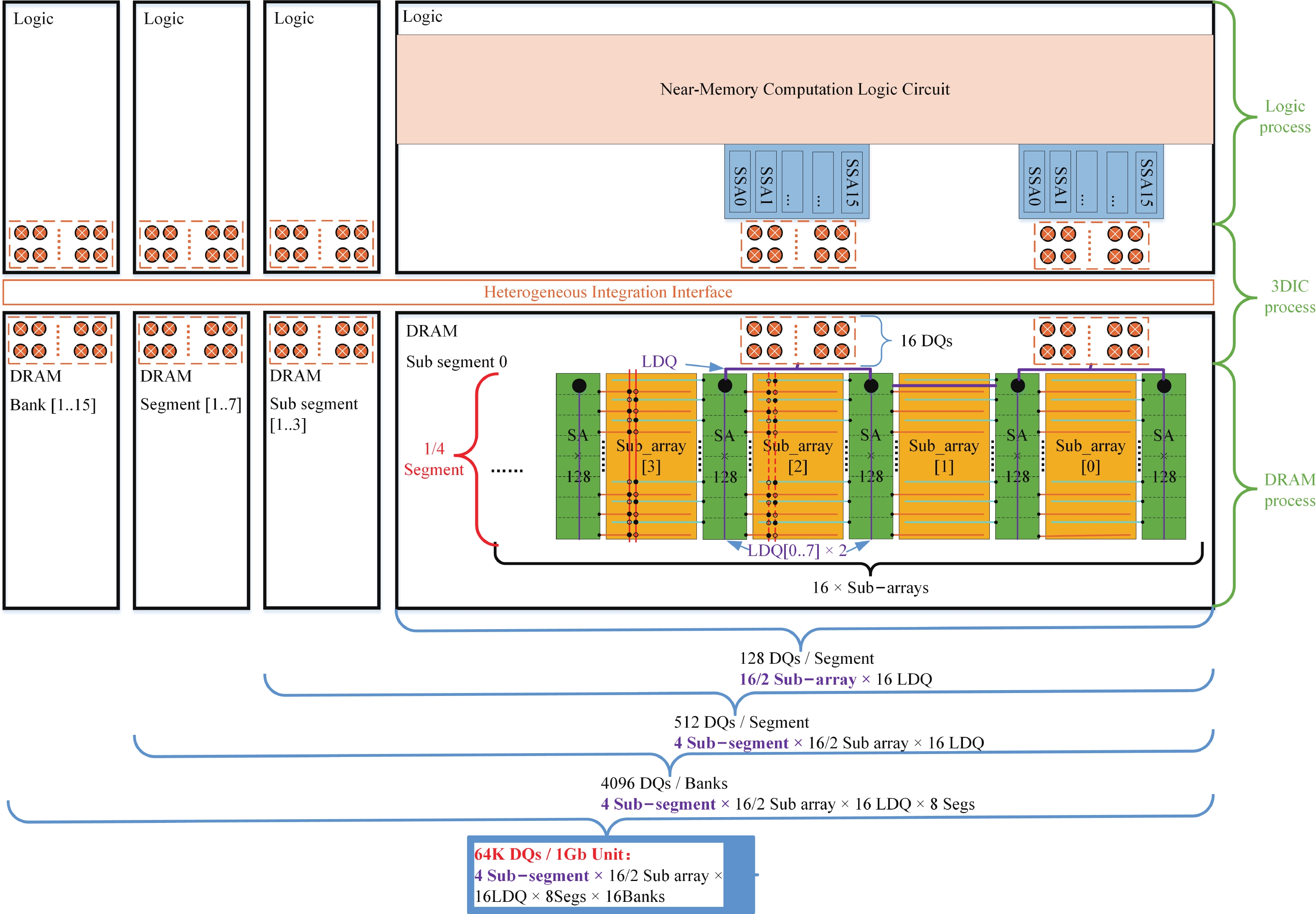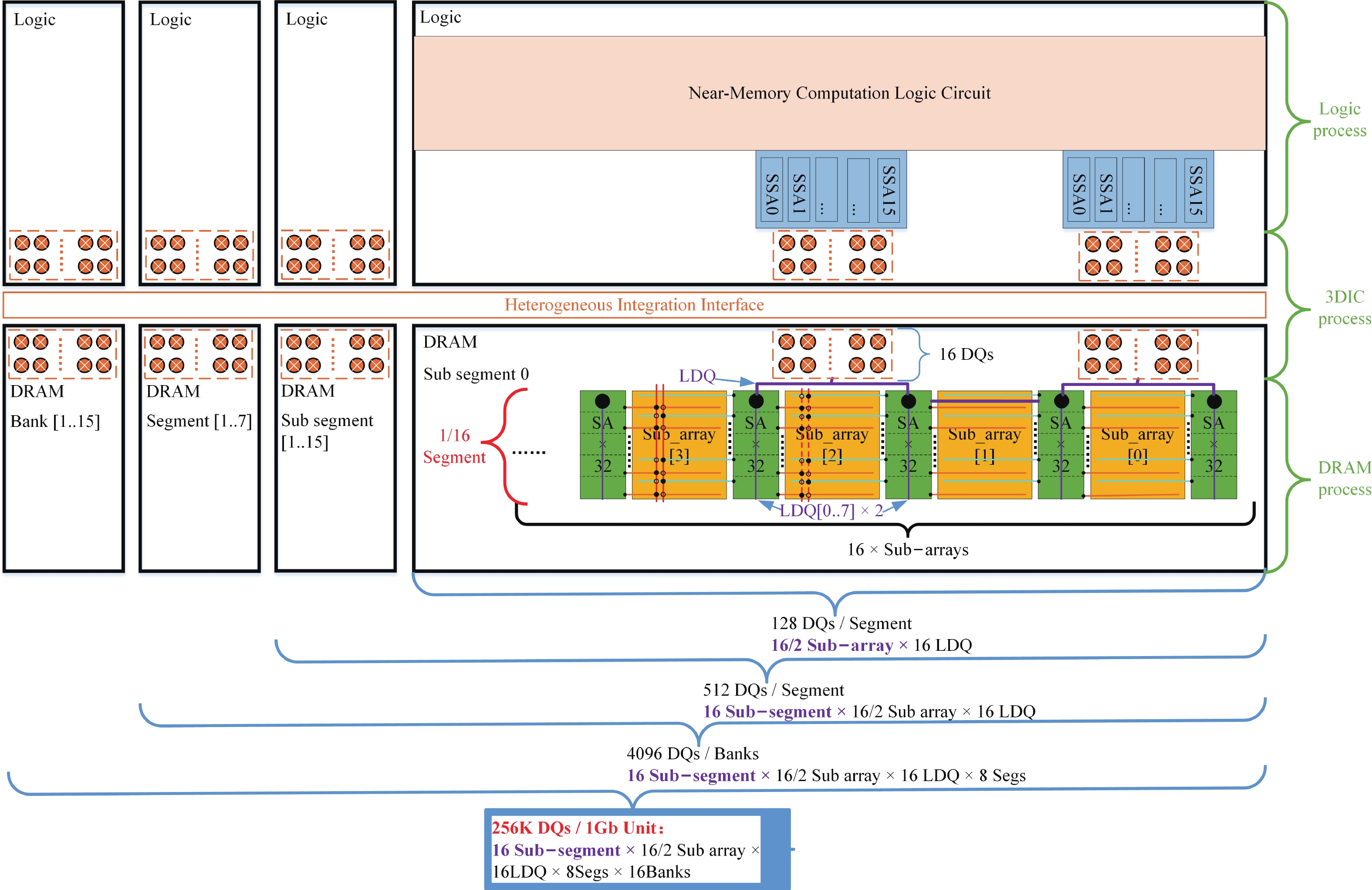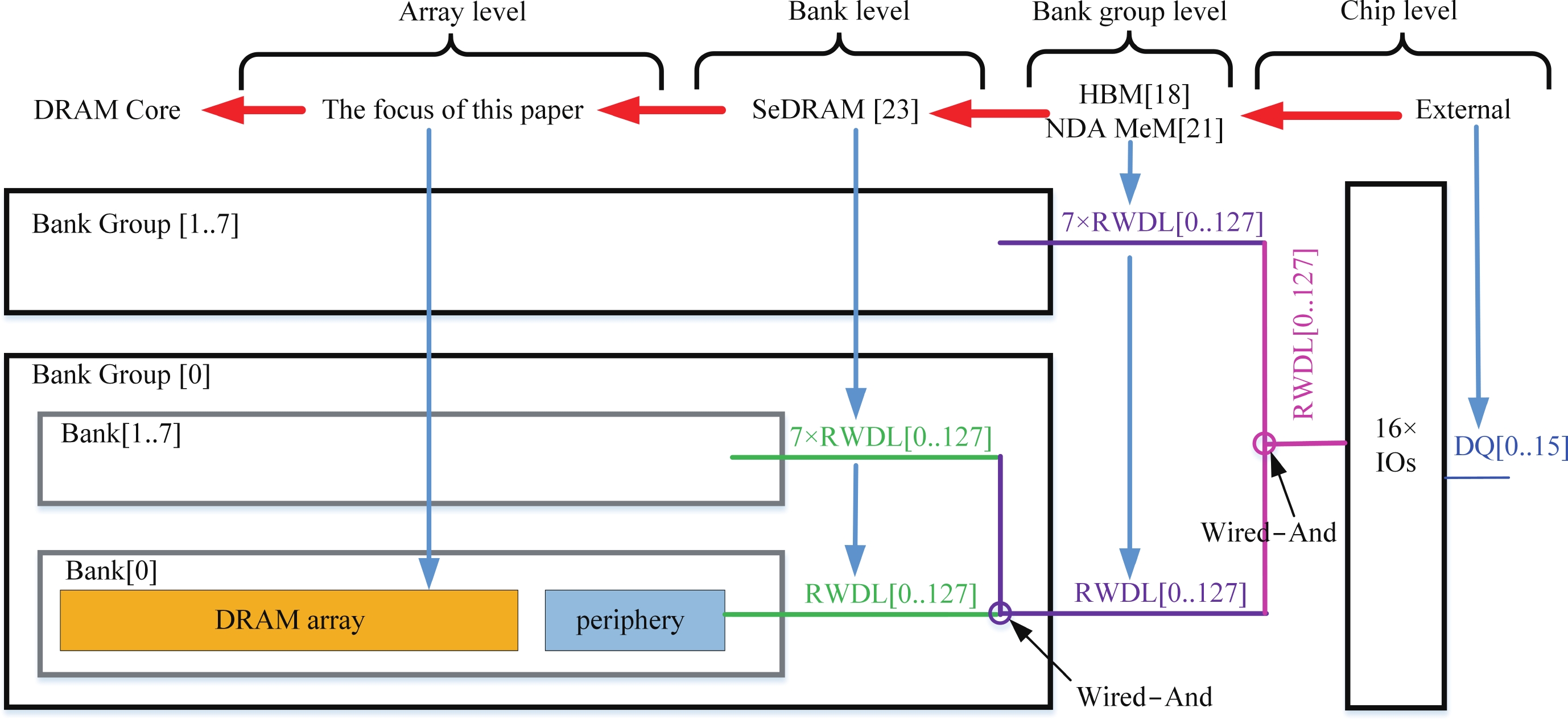
Fig. 1.
(Color online) Near-memory DRAM architectures.
ARTICLES
Xiping Jiang1, 2, 3, , Fujun Bai3, Song Wang3, 4, Yixin Guo3, Fengguo Zuo3, Wenwu Xiao3, Yubing Wang3, Jianguo Yang1, and Ming Liu1, 2
Corresponding author: Xiping Jiang, xiping.jiang@unisemicon.com; Jianguo Yang, yangjianguo@ime.ac.cn
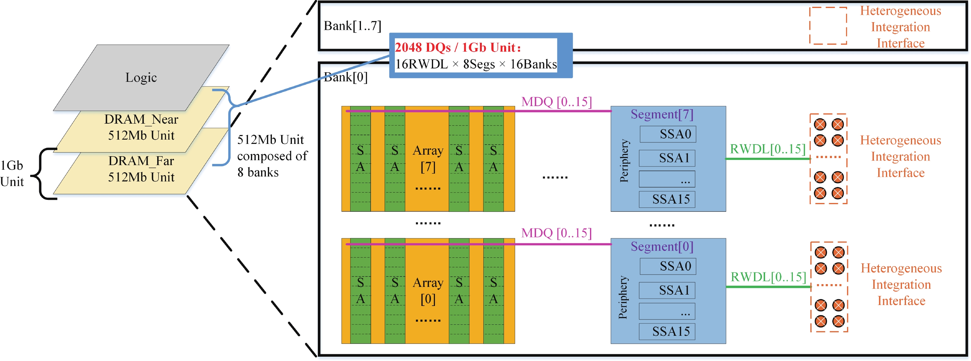
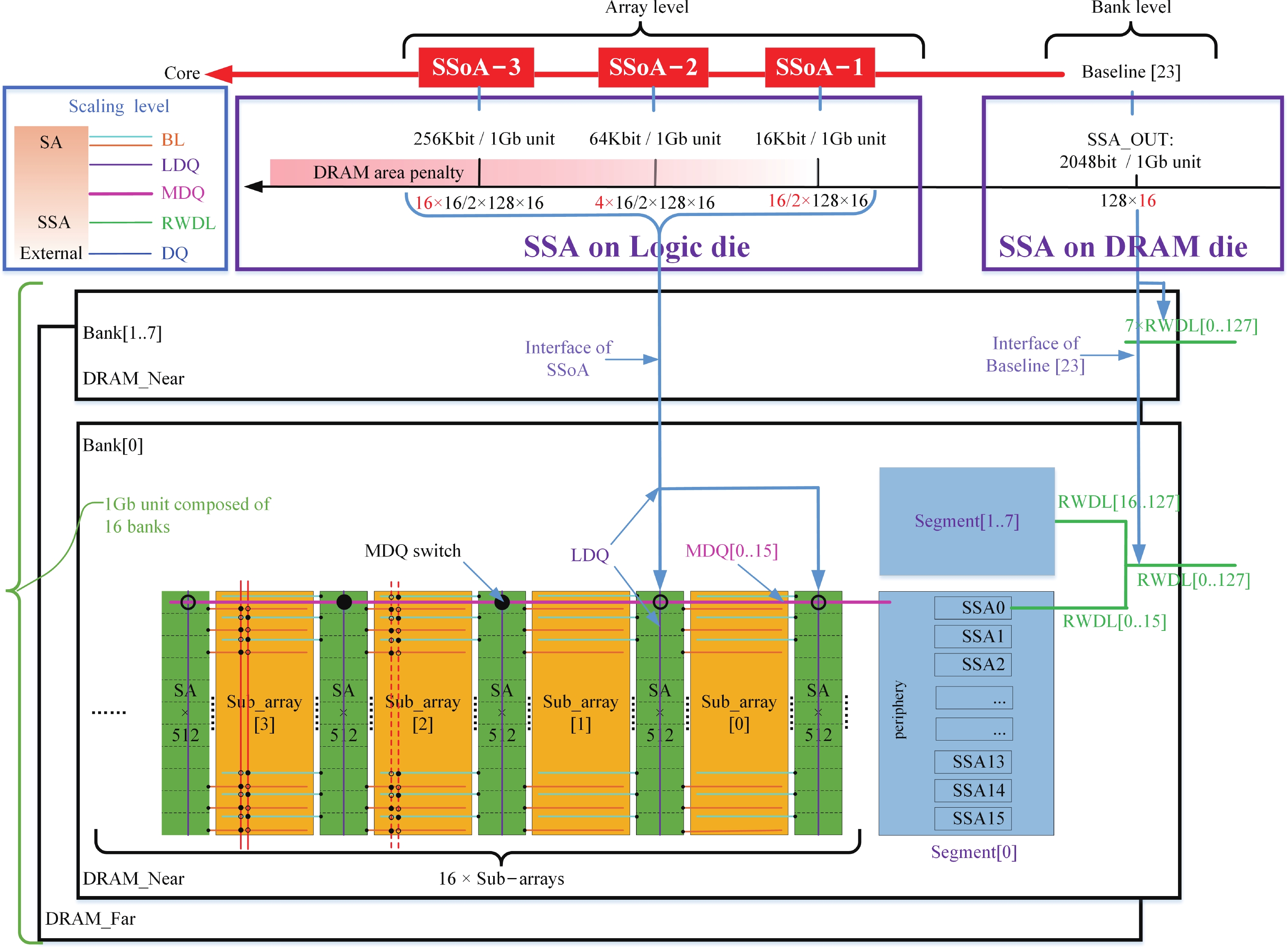
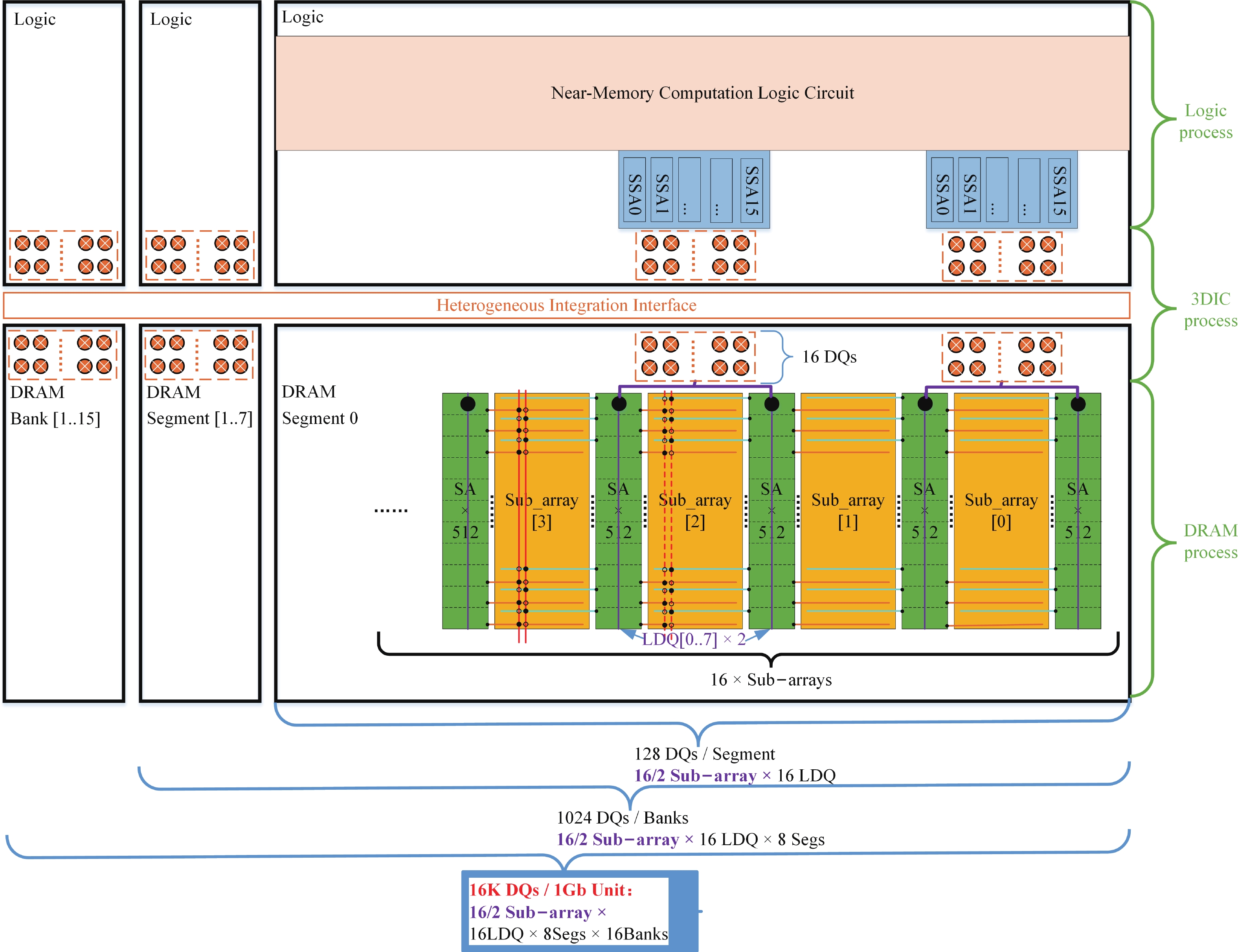
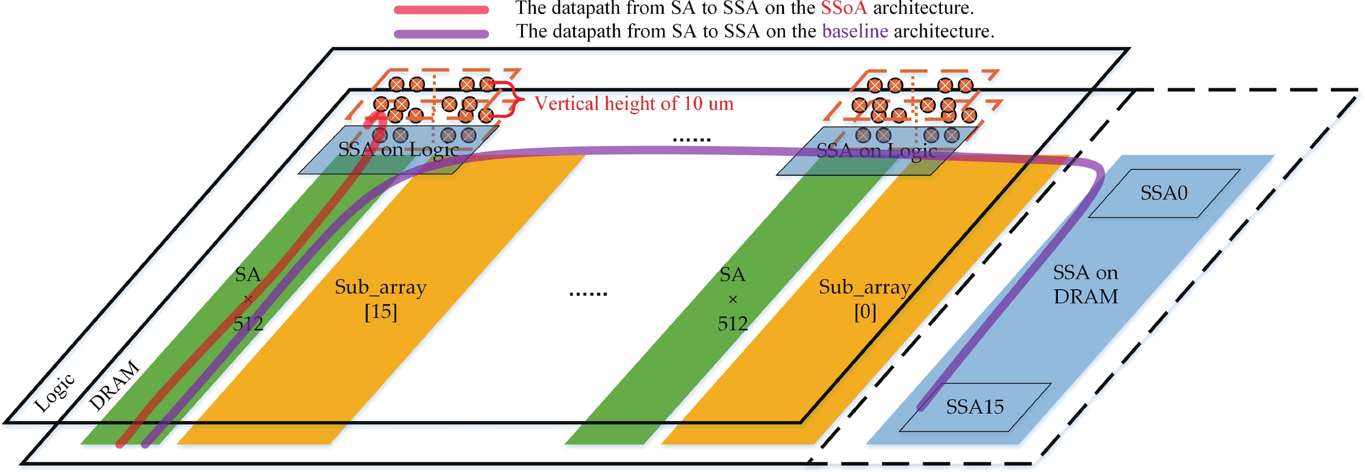
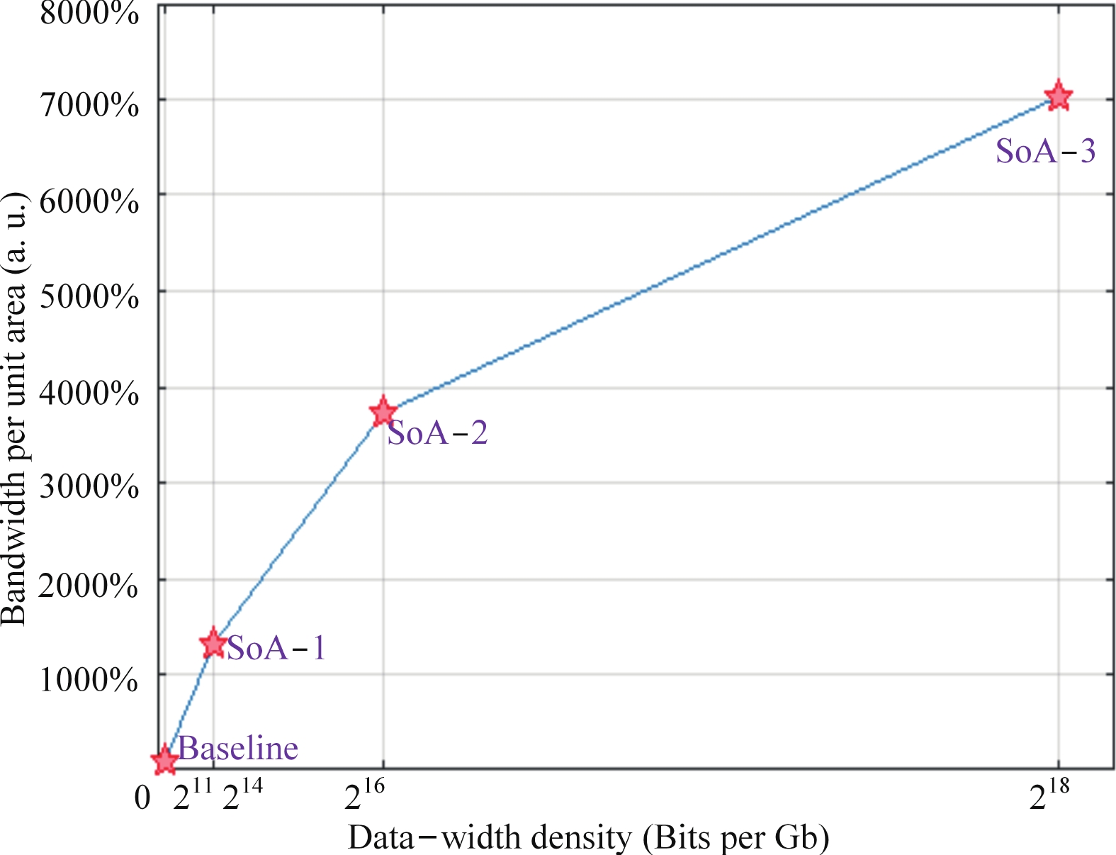
Abstract: Aiming to enhance the bandwidth in near-memory computing, this paper proposes a SSA-over-array (SSoA) architecture. By relocating the secondary sense amplifier (SSA) from dynamic random access memory (DRAM) to the logic die and repositioning the DRAM-to-logic stacking interface closer to the DRAM core, the SSoA overcomes the layout and area limitations of SSA and master DQ (MDQ), leading to improvements in DRAM data-width density and frequency, significantly enhancing bandwidth density. The quantitative evaluation results show a 70.18 times improvement in bandwidth per unit area over the baseline, with a maximum bandwidth of 168.296 Tbps/Gb. We believe the SSoA is poised to redefine near-memory computing development strategies.
Keywords: near-memory, vertical stacking, SSA, bandwidth density
| [1] |
Sebastian A, Le Gallo M, Khaddam-Aljameh R, et al. Memory devices and applications for in-memory computing. Nat Nanotechnol, 2020, 15, 529 doi: 10.1038/s41565-020-0655-z
|
| [2] |
Ielmini D, Wong H S P. In-memory computing with resistive switching devices. Nat Electron, 2018, 1, 333 doi: 10.1038/s41928-018-0092-2
|
| [3] |
Khan K, Pasricha S, Kim R G. A survey of resource management for processing-In-memory and near-memory processing architectures. J Low Power Electron Appl, 2020, 10, 30 doi: 10.3390/jlpea10040030
|
| [4] |
Santoro G, Turvani G, Graziano M. New logic-in-memory paradigms: An architectural and technological perspective. Micromachines, 2019, 10, 368 doi: 10.3390/mi10060368
|
| [5] |
Horowitz M. Computing’s energy problem (and what we can do about it). 2014 IEEE International Solid-State Circuits Conference Digest of Technical Papers (ISSCC), 2014, 10 doi: 10.1109/ISSCC.2014.6757323
|
| [6] |
Ke L, Zhang X, So J, et al. Near-memory processing in action: Accelerating personalized recommendation with AxDIMM. IEEE Micro, 2022, 42, 116 doi: 10.1109/MM.2021.3097700
|
| [7] |
Mutlu O, Ghose S, Gómez-Luna J, et al. Processing data where it makes sense: Enabling in-memory computation. Microprocess Microsyst, 2019, 67, 28 doi: 10.1016/j.micpro.2019.01.009
|
| [8] |
Li Y J, Tang J S, Gao B, et al. Monolithic three-dimensional integration of RRAM-based hybrid memory architecture for one-shot learning. Nat Commun, 2023, 14, 7140 doi: 10.1038/s41467-023-42981-1
|
| [9] |
Sun Z, Kvatinsky S, Si X, et al. A full spectrum of computing-in-memory technologies. Nat Electron, 2023, 6, 823 doi: 10.1038/s41928-023-01053-4
|
| [10] |
Tian W C, Li B, Li Z, et al. Using chiplet encapsulation technology to achieve processing-in-memory functions. Micromachines, 2022, 13, 1790 doi: 10.3390/mi13101790
|
| [11] |
Lee S, Cho H, Son Y H, et al. Leveraging power-performance relationship of energy-efficient modern DRAM devices. IEEE Access, 2018, 6, 31387 doi: 10.1109/ACCESS.2018.2845861
|
| [12] |
Spessot A, Oh H. 1T-1C dynamic random access memory status, challenges, and prospects. IEEE Trans Electron Devices, 2020, 67, 1382 doi: 10.1109/TED.2020.2963911
|
| [13] |
Singh G, Chelini L, Corda S, et al. A review of near-memory computing architectures: Opportunities and challenges. 2018 21st Euromicro Conference on Digital System Design (DSD), 2018, 608 doi: 10.1109/DSD.2018.00106
|
| [14] |
Ravichandiran P P, Franzon P D. A review of 3D-dynamic random-access memory based near-memory computation. 2021 IEEE International 3D Systems Integration Conference (3DIC), 2021, 1 doi: 10.1109/3DIC52383.2021.9687615
|
| [15] |
Yu Y, Jha N K. Energy-efficient monolithic three-dimensional on-chip memory architectures. IEEE Trans Nanotechnol, 2018, 17, 620 doi: 10.1109/TNANO.2017.2731871
|
| [16] |
Asad A, Kaur R, Mohammadi F. A survey on memory subsystems for deep neural network accelerators. Future Internet, 2022, 14, 146 doi: 10.3390/fi14050146
|
| [17] |
Shiba K, Okada M, Kosuge A, et al. A 7-nm FinFET 1.2-TB/s/mm2 3D-stacked SRAM module with 0.7-pJ/b inductive coupling interface using over-SRAM coil and manchester-encoded synchronous transceiver. IEEE J Solid-State Circuits, 2023, 58, 2075 doi: 10.1109/JSSC.2022.3224421
|
| [18] |
Sohn K, Yun W J, Oh R, et al. A 1.2 V20 nm 307 GB/s HBM DRAM with at-speed wafer-level IO test scheme and adaptive refresh considering temperature distribution. IEEE J Solid-State Circuits, 2017, 52, 250 doi: 10.1109/JSSC.2016.2602221
|
| [19] |
OH C S, Chun K C, Byun Y Y, et al. A 1.1V 16GB 640GB/s HBM2E DRAM with a data-bus window-extension technique and a synergetic on-die ECC scheme. 2020 IEEE International Solid-State Circuits Conference Digest of Technical Papers (ISSCC), 2020, 1, 1 doi: 10.1109/ISSCC19947.2020.9063110
|
| [20] |
Park M J, Lee J, Cho K, et al. A 192-gb 12-high 896-GB/s HBM3 DRAM with a TSV auto-calibration scheme and machine-learning-based layout optimization. IEEE J Solid-State Circuits, 2023, 58, 256 doi: 10.1109/JSSC.2022.3193354
|
| [21] |
Farmahini-Farahani A, Ahn J H, Morrow K, et al. NDA: Near-DRAM acceleration architecture leveraging commodity DRAM devices and standard memory modules. 2015 IEEE 21st International Symposium on High Performance Computer Architecture (HPCA), 2015, 283 doi: 10.1109/HPCA.2015.7056040
|
| [22] |
Asghari-Moghaddam H, Farmahini-Farahani A, Morrow K, et al. Near-DRAM acceleration with single-ISA heterogeneous processing in standard memory modules. IEEE Micro, 2016, 36, 24 doi: 10.1109/MM.2016.8
|
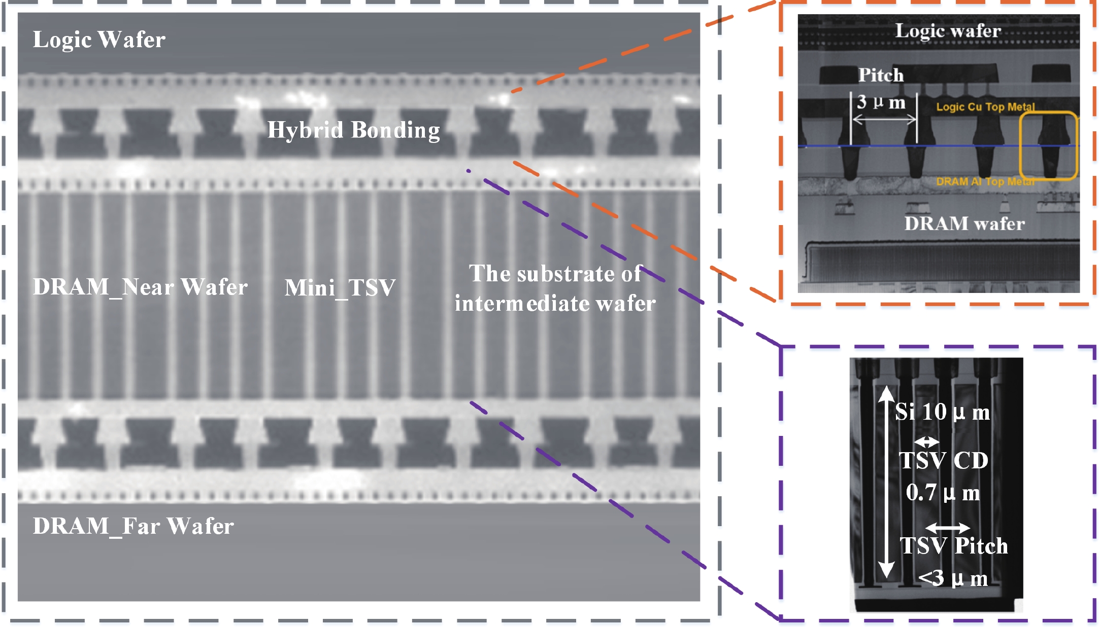
| [23] |
Wang S, Yu B, Xiao W W, et al. A 135 GBps/Gbit 0.66 pJ/bit stacked embedded DRAM with multilayer arrays by fine pitch hybrid bonding and mini-TSV. 2023 IEEE Symposium on VLSI Technology and Circuits (VLSI Technology and Circuits), 2023, 1 doi: 10.23919/VLSITechnologyandCir57934.2023.10185427
|
| [24] |
Niu D M, Li S C, Wang Y H, et al. 184QPS/W 64Mb/mm23D logic-to-DRAM hybrid bonding with process-near-memory engine for recommendation system. 2022 IEEE International Solid-State Circuits Conference (ISSCC), 2022, 1 doi: 10.1109/ISSCC42614.2022.9731694
|
| [25] |
Bai F J, Jiang X P, Wang S, et al. A stacked embedded DRAM array for LPDDR4/4X using hybrid nonding 3D Integration with 34GB/s/1Gb 0.88pJ/b logic-to-memory interface. 2020 IEEE International Electron Devices Meeting (IEDM), 2020, 1, 6.6.1 doi: 10.1109/IEDM13553.2020.9372039
|
| [26] |
Wang S, Jiang X P, Bai F J, et al. A true process-heterogeneous stacked embedded DRAM structure based on wafer-level hybrid bonding. Electronics, 2023, 12, 1077 doi: 10.3390/electronics12051077
|
| [27] |
Park N, Ryu S, Kung J, et al. High-throughput near-memory processing on CNNs with 3D HBM-like memory. ACM Trans on Design Automation of Electronic Systems (TODAES), 2021, 26, 1 doi: 10.1145/3460971
|
| [28] |
Kwon J, Wen S J, Fung R, et al. Temperature estimation of HBM2 channels with tail distribution of retention errors in FPGA-HBM2 platform. Electronics, 2022, 12, 32 doi: 10.3390/electronics12010032
|
| [29] |
Farmahini-Farahani A, Gurumurthi S, Loh G, et al. Challenges of high-capacity DRAM stacks and potential directions. Proceedings of the Workshop on Memory Centric High Performance Computing, 2018, 142535 doi: 10.1145/3286475.32864
|
| [30] |
Son K, Kim S, Park H, et al. Thermal and signal integrity co-design and verification of embedded cooling structure with thermal transmission line for high bandwidth memory module. IEEE Trans Compon Packag Manuf Technol, 2022, 12, 1542 doi: 10.1109/TCPMT.2022.3201673
|
| [31] |
Jiang X P, Jia X R, Wang S, et al. A cross-process signal integrity analysis (CPSIA) method and design optimization for wafer-on-wafer stacked DRAM. Micromachines, 2024, 15, 557 doi: 10.3390/mi15050557
|
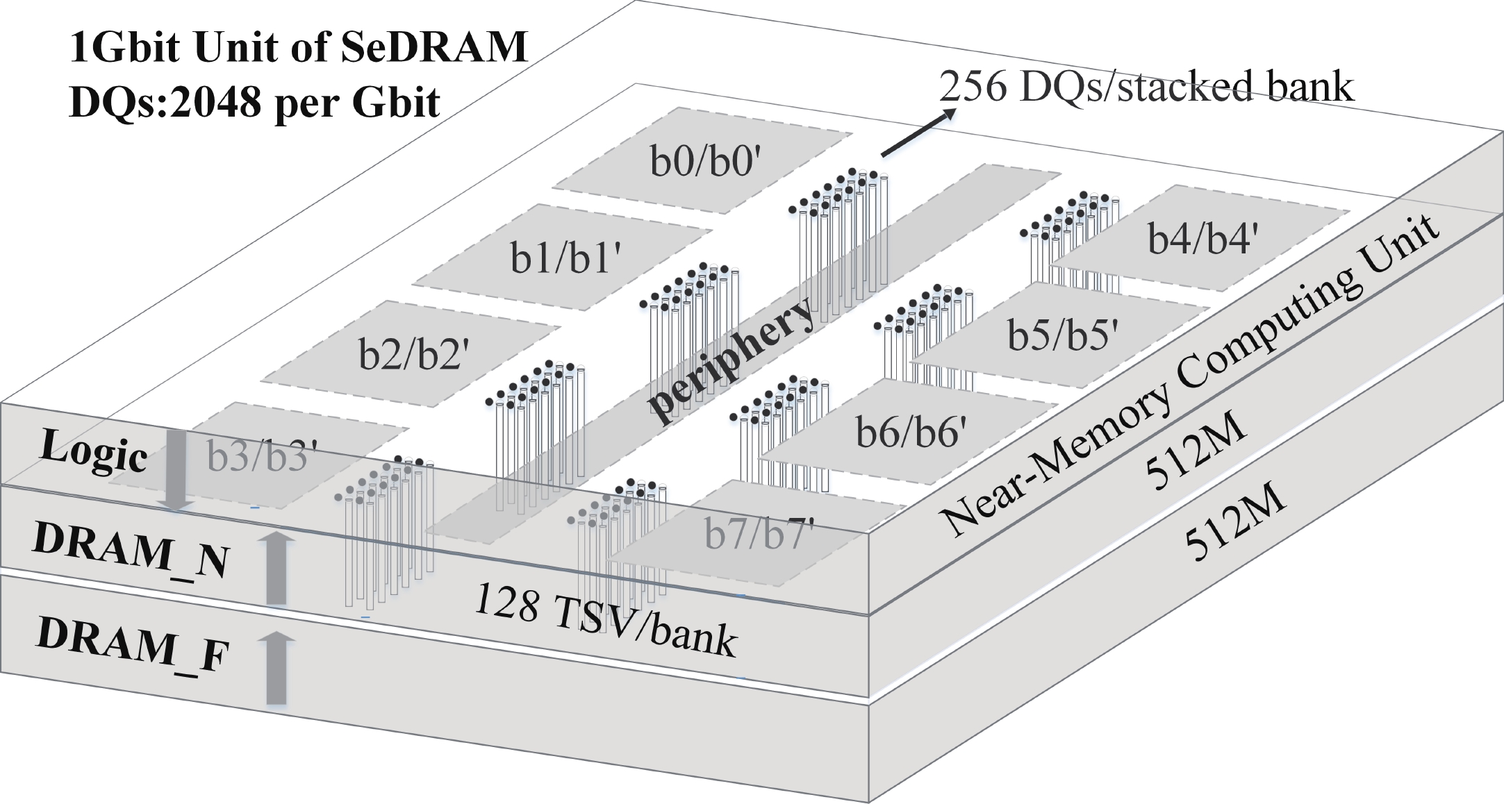

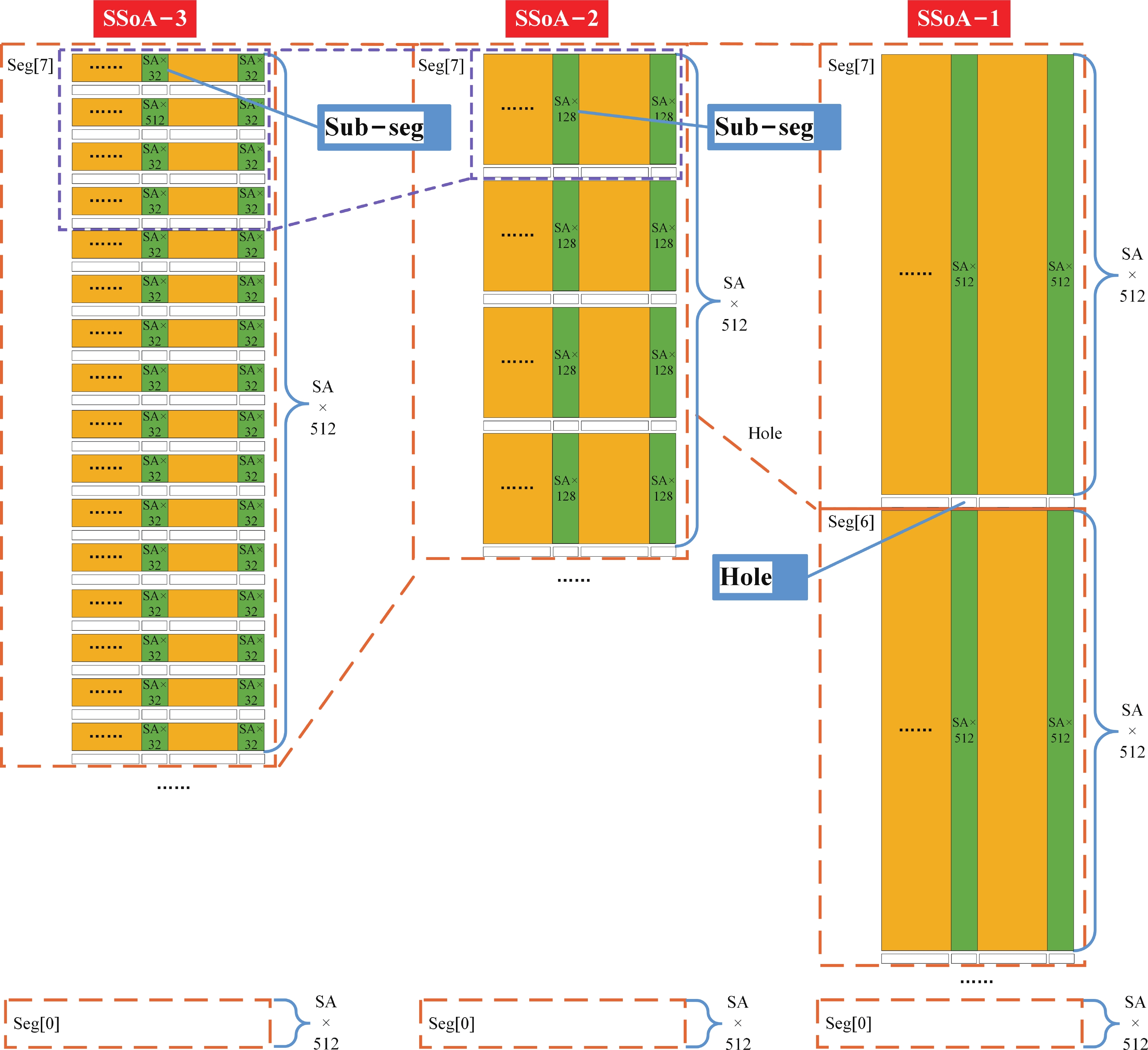
Table 1. DRAM structural parameters.
| Plan | DRAM stacking layer |
Banks per 1 Gb unit |
Segments per bank |
Sub-arrays in horizontal |
LDQ width |
MDQ width |
Sub-segments per segments |
SA group |
Col-address/ sub-array |
| Baseline | 2 | 16 | 8 | 16 | 8 | 16 | 1 | 512 | 5 |
| SSoA-1 | 2 | 16 | 8 | 16 | 8 | None | 1 | 512 | 5 |
| SSoA-2 | 2 | 16 | 8 | 16 | 8 | None | 4 | 128 | 3 |
| SSoA-3 | 2 | 16 | 8 | 16 | 8 | None | 16 | 32 | 1 |
 DownLoad: CSV
Table 2. SSoA-1, SSoA-2, and SSoA-3 structures data-widths on a 1 Gb near-memory unit.
| Plan | LDQs/ sub-array | Sub-arrays/ sub-segment | Sub-segments/ segment | Segments/ bank | Banks/ 1 Gb unit 2) | Data-width/ 1 Gb unit |
| SSoA-1 | 16 | 16/2 1) | 1 | 8 | 16 | 16 384 |
| SSoA-2 | 16 | 16/2 1) | 4 | 8 | 16 | 65 536 |
| SSoA-3 | 16 | 16/2 1) | 16 | 8 | 16 | 262 144 |
| 1) The 16/2 division is due to that the neighboring even and odd SAs are always active at the same time. 2) Derived from double-layered 512 Mb units. | ||||||
DownLoad: CSV
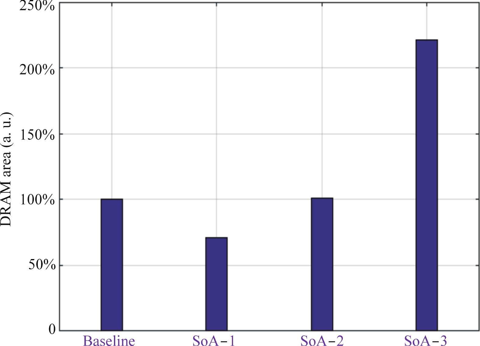
Table 3. Summary of key performance parameters.
| Plan | Tech | Data-width capacity density (Through DQs/Gb) |
Frequency (MHz) |
Bandwidth capacity density (Tbps/Gb)(a. u.) |
DRAM area (a. u.) |
BpA (a. u.) |
| NDA [21] | 28 nm | 128 | 200 | 0.0256 (0.023×) | ~1 | 0.023× |
| Baseline [23] | 25 nm | 2048 | 530 | 1.085 (1×) | 1 | 1× |
| SSoA-1 | 25 nm | 16 384 | 618 | 10.125 (9.33×) | 71% | 13.14× |
| SSoA-2 | 25 nm | 65 536 | 625 | 40.960 (37.75×) | 101% | 37.37× |
| SSoA-3 | 25 nm | 262 144 | 642 | 168.296 (155.1×) | 221% | 70.18× |
DownLoad: CSV
| [1] |
Sebastian A, Le Gallo M, Khaddam-Aljameh R, et al. Memory devices and applications for in-memory computing. Nat Nanotechnol, 2020, 15, 529 doi: 10.1038/s41565-020-0655-z
|
| [2] |
Ielmini D, Wong H S P. In-memory computing with resistive switching devices. Nat Electron, 2018, 1, 333 doi: 10.1038/s41928-018-0092-2
|
| [3] |
Khan K, Pasricha S, Kim R G. A survey of resource management for processing-In-memory and near-memory processing architectures. J Low Power Electron Appl, 2020, 10, 30 doi: 10.3390/jlpea10040030
|
| [4] |
Santoro G, Turvani G, Graziano M. New logic-in-memory paradigms: An architectural and technological perspective. Micromachines, 2019, 10, 368 doi: 10.3390/mi10060368
|
| [5] |
Horowitz M. Computing’s energy problem (and what we can do about it). 2014 IEEE International Solid-State Circuits Conference Digest of Technical Papers (ISSCC), 2014, 10 doi: 10.1109/ISSCC.2014.6757323
|
| [6] |
Ke L, Zhang X, So J, et al. Near-memory processing in action: Accelerating personalized recommendation with AxDIMM. IEEE Micro, 2022, 42, 116 doi: 10.1109/MM.2021.3097700
|
| [7] |
Mutlu O, Ghose S, Gómez-Luna J, et al. Processing data where it makes sense: Enabling in-memory computation. Microprocess Microsyst, 2019, 67, 28 doi: 10.1016/j.micpro.2019.01.009
|
| [8] |
Li Y J, Tang J S, Gao B, et al. Monolithic three-dimensional integration of RRAM-based hybrid memory architecture for one-shot learning. Nat Commun, 2023, 14, 7140 doi: 10.1038/s41467-023-42981-1
|
| [9] |
Sun Z, Kvatinsky S, Si X, et al. A full spectrum of computing-in-memory technologies. Nat Electron, 2023, 6, 823 doi: 10.1038/s41928-023-01053-4
|
| [10] |
Tian W C, Li B, Li Z, et al. Using chiplet encapsulation technology to achieve processing-in-memory functions. Micromachines, 2022, 13, 1790 doi: 10.3390/mi13101790
|
| [11] |
Lee S, Cho H, Son Y H, et al. Leveraging power-performance relationship of energy-efficient modern DRAM devices. IEEE Access, 2018, 6, 31387 doi: 10.1109/ACCESS.2018.2845861
|
| [12] |
Spessot A, Oh H. 1T-1C dynamic random access memory status, challenges, and prospects. IEEE Trans Electron Devices, 2020, 67, 1382 doi: 10.1109/TED.2020.2963911
|
| [13] |
Singh G, Chelini L, Corda S, et al. A review of near-memory computing architectures: Opportunities and challenges. 2018 21st Euromicro Conference on Digital System Design (DSD), 2018, 608 doi: 10.1109/DSD.2018.00106
|
| [14] |
Ravichandiran P P, Franzon P D. A review of 3D-dynamic random-access memory based near-memory computation. 2021 IEEE International 3D Systems Integration Conference (3DIC), 2021, 1 doi: 10.1109/3DIC52383.2021.9687615
|
| [15] |
Yu Y, Jha N K. Energy-efficient monolithic three-dimensional on-chip memory architectures. IEEE Trans Nanotechnol, 2018, 17, 620 doi: 10.1109/TNANO.2017.2731871
|
| [16] |
Asad A, Kaur R, Mohammadi F. A survey on memory subsystems for deep neural network accelerators. Future Internet, 2022, 14, 146 doi: 10.3390/fi14050146
|
| [17] |
Shiba K, Okada M, Kosuge A, et al. A 7-nm FinFET 1.2-TB/s/mm2 3D-stacked SRAM module with 0.7-pJ/b inductive coupling interface using over-SRAM coil and manchester-encoded synchronous transceiver. IEEE J Solid-State Circuits, 2023, 58, 2075 doi: 10.1109/JSSC.2022.3224421
|
| [18] |
Sohn K, Yun W J, Oh R, et al. A 1.2 V20 nm 307 GB/s HBM DRAM with at-speed wafer-level IO test scheme and adaptive refresh considering temperature distribution. IEEE J Solid-State Circuits, 2017, 52, 250 doi: 10.1109/JSSC.2016.2602221
|
| [19] |
OH C S, Chun K C, Byun Y Y, et al. A 1.1V 16GB 640GB/s HBM2E DRAM with a data-bus window-extension technique and a synergetic on-die ECC scheme. 2020 IEEE International Solid-State Circuits Conference Digest of Technical Papers (ISSCC), 2020, 1, 1 doi: 10.1109/ISSCC19947.2020.9063110
|
| [20] |
Park M J, Lee J, Cho K, et al. A 192-gb 12-high 896-GB/s HBM3 DRAM with a TSV auto-calibration scheme and machine-learning-based layout optimization. IEEE J Solid-State Circuits, 2023, 58, 256 doi: 10.1109/JSSC.2022.3193354
|
| [21] |
Farmahini-Farahani A, Ahn J H, Morrow K, et al. NDA: Near-DRAM acceleration architecture leveraging commodity DRAM devices and standard memory modules. 2015 IEEE 21st International Symposium on High Performance Computer Architecture (HPCA), 2015, 283 doi: 10.1109/HPCA.2015.7056040
|
| [22] |
Asghari-Moghaddam H, Farmahini-Farahani A, Morrow K, et al. Near-DRAM acceleration with single-ISA heterogeneous processing in standard memory modules. IEEE Micro, 2016, 36, 24 doi: 10.1109/MM.2016.8
|
| [23] |
Wang S, Yu B, Xiao W W, et al. A 135 GBps/Gbit 0.66 pJ/bit stacked embedded DRAM with multilayer arrays by fine pitch hybrid bonding and mini-TSV. 2023 IEEE Symposium on VLSI Technology and Circuits (VLSI Technology and Circuits), 2023, 1 doi: 10.23919/VLSITechnologyandCir57934.2023.10185427
|
| [24] |
Niu D M, Li S C, Wang Y H, et al. 184QPS/W 64Mb/mm23D logic-to-DRAM hybrid bonding with process-near-memory engine for recommendation system. 2022 IEEE International Solid-State Circuits Conference (ISSCC), 2022, 1 doi: 10.1109/ISSCC42614.2022.9731694
|
| [25] |
Bai F J, Jiang X P, Wang S, et al. A stacked embedded DRAM array for LPDDR4/4X using hybrid nonding 3D Integration with 34GB/s/1Gb 0.88pJ/b logic-to-memory interface. 2020 IEEE International Electron Devices Meeting (IEDM), 2020, 1, 6.6.1 doi: 10.1109/IEDM13553.2020.9372039
|
| [26] |
Wang S, Jiang X P, Bai F J, et al. A true process-heterogeneous stacked embedded DRAM structure based on wafer-level hybrid bonding. Electronics, 2023, 12, 1077 doi: 10.3390/electronics12051077
|
| [27] |
Park N, Ryu S, Kung J, et al. High-throughput near-memory processing on CNNs with 3D HBM-like memory. ACM Trans on Design Automation of Electronic Systems (TODAES), 2021, 26, 1 doi: 10.1145/3460971
|
| [28] |
Kwon J, Wen S J, Fung R, et al. Temperature estimation of HBM2 channels with tail distribution of retention errors in FPGA-HBM2 platform. Electronics, 2022, 12, 32 doi: 10.3390/electronics12010032
|
| [29] |
Farmahini-Farahani A, Gurumurthi S, Loh G, et al. Challenges of high-capacity DRAM stacks and potential directions. Proceedings of the Workshop on Memory Centric High Performance Computing, 2018, 142535 doi: 10.1145/3286475.32864
|
| [30] |
Son K, Kim S, Park H, et al. Thermal and signal integrity co-design and verification of embedded cooling structure with thermal transmission line for high bandwidth memory module. IEEE Trans Compon Packag Manuf Technol, 2022, 12, 1542 doi: 10.1109/TCPMT.2022.3201673
|
| [31] |
Jiang X P, Jia X R, Wang S, et al. A cross-process signal integrity analysis (CPSIA) method and design optimization for wafer-on-wafer stacked DRAM. Micromachines, 2024, 15, 557 doi: 10.3390/mi15050557
|


Article views: 2889 Times PDF downloads: 334 Times Cited by: 0 Times
Received: 02 May 2024 Revised: 04 July 2024 Online: Accepted Manuscript: 01 August 2024Uncorrected proof: 14 August 2024Published: 15 October 2024
| Citation: |
Xiping Jiang, Fujun Bai, Song Wang, Yixin Guo, Fengguo Zuo, Wenwu Xiao, Yubing Wang, Jianguo Yang, Ming Liu. SSA-over-array (SSoA): A stacked DRAM architecture for near-memory computing[J]. Journal of Semiconductors, 2024, 45(10): 102201. doi: 10.1088/1674-4926/24050004
****
X P Jiang, F J Bai, S Wang, Y X Guo, F G Zuo, W W Xiao, Y B Wang, J G Yang, and M Liu, SSA-over-array (SSoA): A stacked DRAM architecture for near-memory computing[J]. J. Semicond., 2024, 45(10), 102201 doi: 10.1088/1674-4926/24050004

|
 Xiping Jiang received his M.S. degree in Computer Science and Technology from Northwestern Polytechnical University, Xi'an, China, in 2003. He is currently a Ph.D. candidate under the supervision of Prof. Ming Liu at University of Chinese Academy of Sciences, Beijing, China. In 2023, he was conferred the title of Professorate Senior Engineer. He is currently working in a leadership role in innovative technology research at Xi'an UniIC Semiconductors. His research interests include emerging memory technologies, near-memory computing, heterogeneous integrated DRAM architecture, and advanced integration technology
 Song Wang received his M.S. degree in Microelectronics and Solid State Electronics from Wuhan University, Wuhan, China, in 2004. He is currently working toward a Ph.D. degree in University of Science and Technology of China. He is working at Xi'an UniIC Semiconductors Co., Ltd. as vice president responsible for memory development. His research interests include high bandwidth DRAM such as GDDR6, HBM, and Stacked Embedded DRAM
 Yixin Guo received his Ph.D. degree in Electronic Science and Technology from Xi’an Jiaotong University, Xi’an, China, in 2019. He is currently working at Xi'an UniIC Semiconductors as a Senior Engineer. His research interests include the architecture and signal integrity of near-memory computing, and memory-bound high performance computing
 Yubing Wang received his M.S. degree from University of Chinese Academy of Sciences, Beijing, China, in 2011. He is working at Xi'an UniIC Semiconductors as a senior director for near-memory computing product line. His research interests include memory and storage controlling methodology and technology, and heterogeneous integration system
 Jianguo Yang received the Ph.D. degree in microelectronics from Fudan University, Shanghai, China, in 2016. In 2016, he joined the Department of Microelectronics, Fudan University, as a Post-Doctoral Research Fellow. In 2019, he joined the Institute of Microelectronics of Chinese Academy of Sciences, Beijing, China, as an Associate Professor. He is currently a Professor in Zhangjiang Laboratory, Shanghai. His research interests include memory circuit design, hardware security, and new computing paradigm
 Ming Liu received the Ph.D. degree in material engineering from the Beijing University of Aeronautics and Astronauts, Beijing, China, in 1998. She joined the Institute of Microelectronics of the Chinese Academy of Sciences, Beijing, in 1999, where she became a Full Professor in 2000. She was selected as an Academician of the Chinese Academy of Sciences, Beijing, in 2015. She was the Director of the Key Laboratory of Microelectronics Devices and Integrated Technology, Institute of Microelectronics of the Chinese Academy of Sciences. Currently, she is the Director with the Frontier Institute of Chip and System, State Key Laboratory of Integrated Chips and Systems, Fudan University, Shanghai, China. Her research areas include advanced semiconductor process, emerging memory and logic technologies, novel integration and package technology, and next-generation computing paradigms
| [1] |
Sebastian A, Le Gallo M, Khaddam-Aljameh R, et al. Memory devices and applications for in-memory computing. Nat Nanotechnol, 2020, 15, 529 doi: 10.1038/s41565-020-0655-z
|
| [2] |
Ielmini D, Wong H S P. In-memory computing with resistive switching devices. Nat Electron, 2018, 1, 333 doi: 10.1038/s41928-018-0092-2
|
| [3] |
Khan K, Pasricha S, Kim R G. A survey of resource management for processing-In-memory and near-memory processing architectures. J Low Power Electron Appl, 2020, 10, 30 doi: 10.3390/jlpea10040030
|
| [4] |
Santoro G, Turvani G, Graziano M. New logic-in-memory paradigms: An architectural and technological perspective. Micromachines, 2019, 10, 368 doi: 10.3390/mi10060368
|
| [5] |
Horowitz M. Computing’s energy problem (and what we can do about it). 2014 IEEE International Solid-State Circuits Conference Digest of Technical Papers (ISSCC), 2014, 10 doi: 10.1109/ISSCC.2014.6757323
|
| [6] |
Ke L, Zhang X, So J, et al. Near-memory processing in action: Accelerating personalized recommendation with AxDIMM. IEEE Micro, 2022, 42, 116 doi: 10.1109/MM.2021.3097700
|
| [7] |
Mutlu O, Ghose S, Gómez-Luna J, et al. Processing data where it makes sense: Enabling in-memory computation. Microprocess Microsyst, 2019, 67, 28 doi: 10.1016/j.micpro.2019.01.009
|
| [8] |
Li Y J, Tang J S, Gao B, et al. Monolithic three-dimensional integration of RRAM-based hybrid memory architecture for one-shot learning. Nat Commun, 2023, 14, 7140 doi: 10.1038/s41467-023-42981-1
|
| [9] |
Sun Z, Kvatinsky S, Si X, et al. A full spectrum of computing-in-memory technologies. Nat Electron, 2023, 6, 823 doi: 10.1038/s41928-023-01053-4
|
| [10] |
Tian W C, Li B, Li Z, et al. Using chiplet encapsulation technology to achieve processing-in-memory functions. Micromachines, 2022, 13, 1790 doi: 10.3390/mi13101790
|
| [11] |
Lee S, Cho H, Son Y H, et al. Leveraging power-performance relationship of energy-efficient modern DRAM devices. IEEE Access, 2018, 6, 31387 doi: 10.1109/ACCESS.2018.2845861
|
| [12] |
Spessot A, Oh H. 1T-1C dynamic random access memory status, challenges, and prospects. IEEE Trans Electron Devices, 2020, 67, 1382 doi: 10.1109/TED.2020.2963911
|
| [13] |
Singh G, Chelini L, Corda S, et al. A review of near-memory computing architectures: Opportunities and challenges. 2018 21st Euromicro Conference on Digital System Design (DSD), 2018, 608 doi: 10.1109/DSD.2018.00106
|
| [14] |
Ravichandiran P P, Franzon P D. A review of 3D-dynamic random-access memory based near-memory computation. 2021 IEEE International 3D Systems Integration Conference (3DIC), 2021, 1 doi: 10.1109/3DIC52383.2021.9687615
|
| [15] |
Yu Y, Jha N K. Energy-efficient monolithic three-dimensional on-chip memory architectures. IEEE Trans Nanotechnol, 2018, 17, 620 doi: 10.1109/TNANO.2017.2731871
|
| [16] |
Asad A, Kaur R, Mohammadi F. A survey on memory subsystems for deep neural network accelerators. Future Internet, 2022, 14, 146 doi: 10.3390/fi14050146
|
| [17] |
Shiba K, Okada M, Kosuge A, et al. A 7-nm FinFET 1.2-TB/s/mm2 3D-stacked SRAM module with 0.7-pJ/b inductive coupling interface using over-SRAM coil and manchester-encoded synchronous transceiver. IEEE J Solid-State Circuits, 2023, 58, 2075 doi: 10.1109/JSSC.2022.3224421
|
| [18] |
Sohn K, Yun W J, Oh R, et al. A 1.2 V20 nm 307 GB/s HBM DRAM with at-speed wafer-level IO test scheme and adaptive refresh considering temperature distribution. IEEE J Solid-State Circuits, 2017, 52, 250 doi: 10.1109/JSSC.2016.2602221
|
| [19] |
OH C S, Chun K C, Byun Y Y, et al. A 1.1V 16GB 640GB/s HBM2E DRAM with a data-bus window-extension technique and a synergetic on-die ECC scheme. 2020 IEEE International Solid-State Circuits Conference Digest of Technical Papers (ISSCC), 2020, 1, 1 doi: 10.1109/ISSCC19947.2020.9063110
|
| [20] |
Park M J, Lee J, Cho K, et al. A 192-gb 12-high 896-GB/s HBM3 DRAM with a TSV auto-calibration scheme and machine-learning-based layout optimization. IEEE J Solid-State Circuits, 2023, 58, 256 doi: 10.1109/JSSC.2022.3193354
|
| [21] |
Farmahini-Farahani A, Ahn J H, Morrow K, et al. NDA: Near-DRAM acceleration architecture leveraging commodity DRAM devices and standard memory modules. 2015 IEEE 21st International Symposium on High Performance Computer Architecture (HPCA), 2015, 283 doi: 10.1109/HPCA.2015.7056040
|
| [22] |
Asghari-Moghaddam H, Farmahini-Farahani A, Morrow K, et al. Near-DRAM acceleration with single-ISA heterogeneous processing in standard memory modules. IEEE Micro, 2016, 36, 24 doi: 10.1109/MM.2016.8
|
| [23] |
Wang S, Yu B, Xiao W W, et al. A 135 GBps/Gbit 0.66 pJ/bit stacked embedded DRAM with multilayer arrays by fine pitch hybrid bonding and mini-TSV. 2023 IEEE Symposium on VLSI Technology and Circuits (VLSI Technology and Circuits), 2023, 1 doi: 10.23919/VLSITechnologyandCir57934.2023.10185427
|
| [24] |
Niu D M, Li S C, Wang Y H, et al. 184QPS/W 64Mb/mm23D logic-to-DRAM hybrid bonding with process-near-memory engine for recommendation system. 2022 IEEE International Solid-State Circuits Conference (ISSCC), 2022, 1 doi: 10.1109/ISSCC42614.2022.9731694
|
| [25] |
Bai F J, Jiang X P, Wang S, et al. A stacked embedded DRAM array for LPDDR4/4X using hybrid nonding 3D Integration with 34GB/s/1Gb 0.88pJ/b logic-to-memory interface. 2020 IEEE International Electron Devices Meeting (IEDM), 2020, 1, 6.6.1 doi: 10.1109/IEDM13553.2020.9372039
|
| [26] |
Wang S, Jiang X P, Bai F J, et al. A true process-heterogeneous stacked embedded DRAM structure based on wafer-level hybrid bonding. Electronics, 2023, 12, 1077 doi: 10.3390/electronics12051077
|
| [27] |
Park N, Ryu S, Kung J, et al. High-throughput near-memory processing on CNNs with 3D HBM-like memory. ACM Trans on Design Automation of Electronic Systems (TODAES), 2021, 26, 1 doi: 10.1145/3460971
|
| [28] |
Kwon J, Wen S J, Fung R, et al. Temperature estimation of HBM2 channels with tail distribution of retention errors in FPGA-HBM2 platform. Electronics, 2022, 12, 32 doi: 10.3390/electronics12010032
|
| [29] |
Farmahini-Farahani A, Gurumurthi S, Loh G, et al. Challenges of high-capacity DRAM stacks and potential directions. Proceedings of the Workshop on Memory Centric High Performance Computing, 2018, 142535 doi: 10.1145/3286475.32864
|
| [30] |
Son K, Kim S, Park H, et al. Thermal and signal integrity co-design and verification of embedded cooling structure with thermal transmission line for high bandwidth memory module. IEEE Trans Compon Packag Manuf Technol, 2022, 12, 1542 doi: 10.1109/TCPMT.2022.3201673
|
| [31] |
Jiang X P, Jia X R, Wang S, et al. A cross-process signal integrity analysis (CPSIA) method and design optimization for wafer-on-wafer stacked DRAM. Micromachines, 2024, 15, 557 doi: 10.3390/mi15050557
|

 WeChat ID
Journal of Semiconductors © 2017 All Rights Reserved 京ICP备05085259号-2