| Citation: |
Yingjie Wang, Sen Huang, Qimeng Jiang, Jiaolong Liu, Xinhua Wang, Wen Liu, Liu Wang, Jingyuan Shi, Jie Fan, Xinguo Gao, Haibo Yin, Ke Wei, Xinyu Liu. First demonstration of a self-aligned p-channel GaN back gate injection transistor[J]. Journal of Semiconductors, 2024, 45(11): 112502. doi: 10.1088/1674-4926/24050027
****
Y J Wang, S Huang, Q M Jiang, J L Liu, X H Wang, W Liu, L Wang, J Y Shi, J Fan, X G Gao, H B Yin, K Wei, and X Y Liu, First demonstration of a self-aligned p-channel GaN back gate injection transistor[J]. J. Semicond., 2024, 45(11), 112502 doi: 10.1088/1674-4926/24050027
|
First demonstration of a self-aligned p-channel GaN back gate injection transistor
DOI: 10.1088/1674-4926/24050027
More Information
-
Abstract
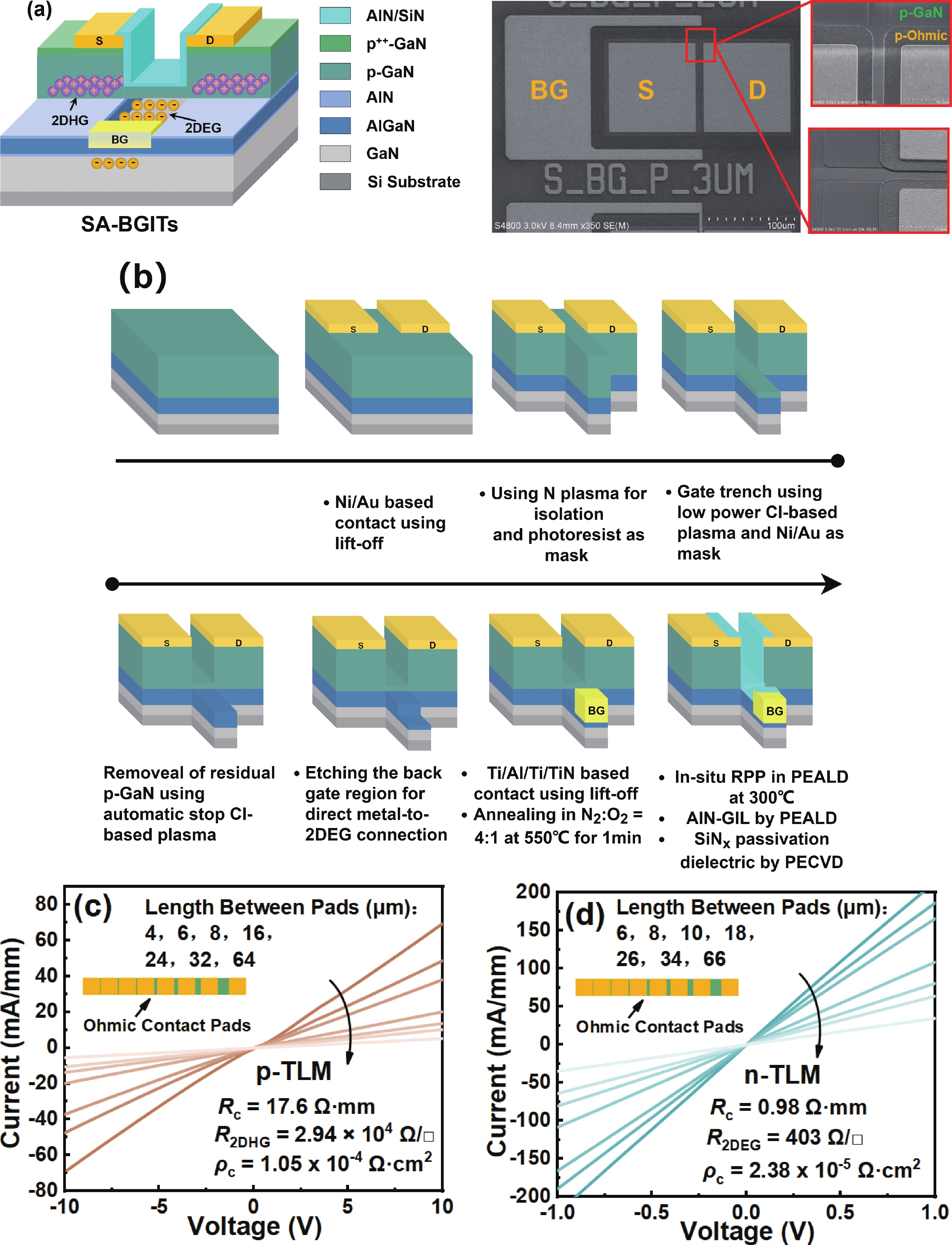
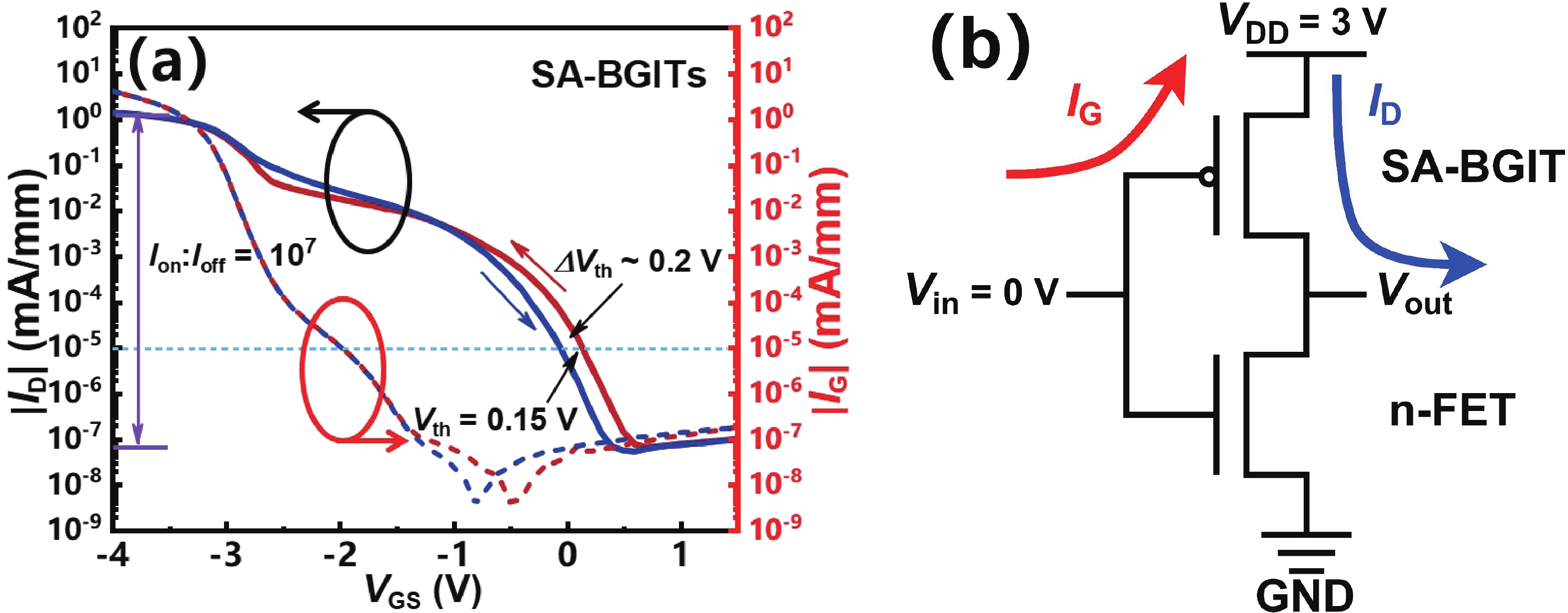
In this study, we present the development of self-aligned p-channel GaN back gate injection transistors (SA-BGITs) that exhibit a high ON-state current. This achievement is primarily attributed to the conductivity modulation effect of the 2-D electron gas (2DEG, the back gate) beneath the 2-D hole gas (2DHG) channel. SA-BGITs with a gate length of 1 μm have achieved an impressive peak drain current (ID,MAX) of 9.9 mA/mm. The fabricated SA-BGITs also possess a threshold voltage of 0.15 V, an exceptionally minimal threshold hysteresis of 0.2 V, a high switching ratio of 107, and a reduced ON-resistance (RON) of 548 Ω·mm. Additionally, the SA-BGITs exhibit a steep sub-threshold swing (SS) of 173 mV/dec, further highlighting their suitability for integration into GaN logic circuits.-
Keywords:
- GaN,
- p-FETs,
- self-alignment,
- back gate,
- threshold hysteresis,
- conductivity modulation
-
References
[1] Luo F, Chen Z, Xue L X, et al. Design considerations for GaN HEMT multichip halfbridge module for high-frequency power converters. 2014 IEEE Applied Power Electronics Conference and Exposition-APEC, 2014, 537 doi: 10.1109/APEC.2014.6803361[2] Chen K J, Wei J, Tang G F, et al. Planar GaN power integration-The world is flat. 2020 IEEE International Electron Devices Meeting (IEDM), 2020, 27.1.1 doi: 10.1109/IEDM13553.2020.9372069[3] Du C L, Ye R, Cai X L, et al. A review on GaN HEMTs: nonlinear mechanisms and improvement methods. Journal of Semiconductors, 2023, 44, 121801 doi: 10.1088/1674-4926/44/12/121801[4] Chowdhury N, Xie Q Y, Yuan M Y, et al. First demonstration of a self-aligned GaN p-FET. 2019 IEEE International Electron Devices Meeting (IEDM), 2019, 4.6.1 doi: 10.1109/IEDM19573.2019.8993569[5] Wei J, Zheng Z Y, Tang G F, et al. GaN power integration technology and its future prospects. IEEE Trans Electron Devices, 2024, 71, 1365 doi: 10.1109/TED.2023.3341053[6] Ajayan J, Nirmal D, Mohankumar P, et al. Challenges in material processing and reliability issues in AlGaN/GaN HEMTs on silicon wafers for future RF power electronics & switching applications: A critical review. Materials Science in Semiconductor Processing, 2022, 151, 106982 doi: 10.1016/j.mssp.2022.106982[7] Mounika B, Ajayan J, Bhattacharya S, et al. Recent developments in materials, architectures and processing of AlGaN/GaN HEMTs for future RF and power electronic applications: A critical review. Micro Nanostruct, 2022, 168, 207317 doi: 10.1016/j.micrna.2022.207317[8] Zheng Z Y, Zhang L, Song W J, et al. Gallium nitride-based complementary logic integrated circuits. Nat Electron, 2021, 4, 595 doi: 10.1038/s41928-021-00611-y[9] Chowdhury N, Xie Q Y, Yuan M Y, et al. Regrowth-free GaN-based complementary logic on a Si substrate. IEEE Electron Device Lett, 2020, 41, 820 doi: 10.1109/LED.2020.2987003[10] Ujita S, Kinoshita Y, Umeda H, et al. A compact GaN-based DC-DC converter IC with high-speed gate drivers enabling high efficiencies. 2014 IEEE 26th International Symposium on Power Semiconductor Devices & IC’s (ISPSD), 2014, 51 doi: 10.1109/ISPSD.2014.6855973[11] Zhu M H, Matioli E. Monolithic integration of GaN-based NMOS digital logic gate circuits with E-mode power GaN MOSHEMTs. 2018 IEEE 30th International Symposium on Power Semiconductor Devices and ICs (ISPSD), 2018, 236 doi: 10.1109/ISPSD.2018.8393646[12] Kaufmann U, Schlotter P, Obloh H, et al. Hole conductivity and compensation in epitaxial GaN: Mg layers. Phys Rev B, 2000, 62, 10867 doi: 10.1103/PhysRevB.62.10867[13] Poncé S, Jena D, Giustino F. Hole mobility of strained GaN from first principles. Phys Rev B, 2019, 100, 085204 doi: 10.1103/PhysRevB.100.085204[14] Lancefield D, Eshghi H. Temperature-dependent hole transport in GaN. J Phys: Condens Matter, 2001, 13, 8939 doi: 10.1088/0953-8984/13/40/308[15] Tang J J, Jiang Z H, Wang C C, et al. Bipolar p-FET with enhanced conduction capability on E-mode GaN-on-Si HEMT platform. 2023 IEEE International Electron Devices Meeting (IEDM), 2023, 1 doi: 10.1109/IEDM45741.2023.10413728[16] Raj A, Krishna A, Romanczyk B, et al. GaN/AlGaN superlattice based E-mode hole channel FinFET with Schottky gate. IEEE Electron Device Lett, 2023, 44, 9 doi: 10.1109/LED.2022.3223331[17] Xie Q Y, Yuan M Y, Niroula J, et al. Highly-scaled self-aligned GaN complementary technology on a GaN-on-Si platform. 2022 International Electron Devices Meeting (IEDM), 2022, 35.3.1 doi: 10.1109/IEDM45625.2022.10019401[18] Shinohara K, Regan D, Corrion A, et al. Deeply-scaled self-aligned-gate GaN DH-HEMTs with ultrahigh cutoff frequency. 2011 IEEE International Electron Devices Meeting (IEDM), 2011, 19.1.1 doi: 10.1109/IEDM.2011.6131582[19] Chen T, Zheng Z Y, Feng S R, et al. Endurance improvement of GaN bipolar charge trapping memory with back gate injection. IEEE Electron Device Lett, 2023, 44, 1408 doi: 10.1109/LED.2023.3299961[20] Jin H, Jiang Q M, Huang S, et al. An enhancement-mode GaN p-FET with improved breakdown voltage. IEEE Electron Device Lett, 2022, 43, 1191 doi: 10.1109/LED.2022.3184998[21] Huang S, Jiang Q M, Yang S, et al. Effective passivation of AlGaN/GaN HEMTs by ALD-grown AlN thin film. IEEE Electron Device Lett, 2012, 33, 516 doi: 10.1109/LED.2012.2185921[22] Nakajima A, Liu P C, Ogura M, et al. Generation and transportation mechanisms for two-dimensional hole gases in GaN/AlGaN/GaN double heterostructures. J Appl Phys, 2014, 115, 153707 doi: 10.1063/1.4872242[23] Uemoto Y, Hikita M, Ueno H, et al. Gate injection transistor (GIT)—a normally-off AlGaN/GaN power transistor using conductivity modulation. IEEE Trans Electron Devices, 2007, 54, 3393 doi: 10.1109/TED.2007.908601[24] Bandić Z Z, Bridger P M, Piquette E C, et al. Electron diffusion length and lifetime in p-type GaN. Appl Phys Lett, 1998, 73, 3276 doi: 10.1063/1.122743[25] Bandić Z Z, Bridger P M, Piquette E C, et al. Minority carrier diffusion length and lifetime in GaN. Appl Phys Lett, 1998, 72, 3166 doi: 10.1063/1.121581[26] Hacke P, Nakayama H, Detchprohm T, et al. Deep levels in the upper band-gap region of lightly Mg-doped GaN. Appl Phys Lett, 1996, 68, 1362 doi: 10.1063/1.116080[27] Zhang L, Zheng Z Y, Cheng Y, et al. SiN/in-situ-GaON staggered gate stack on p-GaN for enhanced stability in buried-channel GaN p-FETs. 2021 IEEE International Electron Devices Meeting (IEDM), 2021, 5.3.1 doi: 10.1109/IEDM19574.2021.9720653[28] Wang L, Huang S, Jiang Q M, et al. High threshold voltage stability enhancement-mode GaN p-FETs fabricated with PEALD-AlN gate interfacial layer. IEEE Electron Device Lett, 2024, 45, 320 doi: 10.1109/LED.2024.3354935[29] Spijkman M J, Myny K, Smits E C P, et al. Dual-gate thin-film transistors, integrated circuits and sensors. Adv Mater, 2011, 23, 3231 doi: 10.1002/adma.201101493[30] Wu X Y, Cott D, Lin Z Y, et al. Dual gate synthetic MoS2 MOSFETs with 4.56 µF/cm2 channel capacitance, 320 µS/µm Gm and 420 µA/µm Id at 1 V Vd/100nm Lg. 2021 IEEE International Electron Devices Meeting (IEDM), 2021, 7.4.1 doi: 10.1109/IEDM19574.2021.9720695[31] Chowdhury N, Xie Q Y, Niroula J, et al. Field-induced acceptor ionization in enhancement-mode GaN p-MOSFETs. 2020 IEEE International Electron Devices Meeting (IEDM), 2020, 5.5.1 doi: 10.1109/IEDM13553.2020.9371963[32] Li G W, Wang R H, Song B, et al. Polarization-induced GaN-on-insulator E/D mode p-channel heterostructure FETs. IEEE Electron Device Lett, 2013, 34, 852 doi: 10.1109/LED.2013.2264311[33] Chu R M, Cao Y, Chen M, et al. An experimental demonstration of GaN CMOS technology. IEEE Electron Device Lett, 2016, 37, 269 doi: 10.1109/LED.2016.2515103[34] Li T, Zhang M, Yu J J, et al. Development of enhancement-mode GaN p-FET with post-etch wet treatment on p-GaN gate HEMT epi-wafer. IEEE Trans Electron Devices, 2024, 71, 2361 doi: 10.1109/TED.2024.3365676[35] Su H K, Zhang T, Xu S R, et al. Normally-off p-channel AlGaN/GaN/AlGaN MESFET with high breakdown voltage and ultra-low interface state density. IEEE Electron Device Lett, 2023, 44, 1939 doi: 10.1109/LED.2023.3323497[36] Gao X T, Yu G H, Zhou J A, et al. Study of enhancement-mode GaN pFET with H plasma treated gate recess. J Semicond, 2023, 44, 112801 doi: 10.1088/1674-4926/44/11/112801[37] Jin H, Huang S, Jiang Q M, et al. High-performance enhancement-mode GaN-based p-FETs fabricated with O3-Al2O3/HfO2-stacked gate dielectric. Journal of Semiconductors, 2023, 44, 102801 doi: 10.1088/1674-4926/44/10/102801 -
Proportional views


 Yingjie Wang received his BS degree from the Huazhong University of Science and Technology, Wuhan, China, in 2018. He is pursuing a PhD degree at the Institute of Microelectronics, Chinese Academy of Science, Beijing. His research focuses on fabrication and monolithic integration of GaN devices.
 Sen Huang received his PhD degree from Peking University, Beijing, China, in 2009. He is currently a professor at the Institute of Microelectronics, Chinese Academy of Sciences, Beijing. His current research interests include advanced design, fabrication, and characterization technologies for Ⅲ–Ⅴ power semiconductor devices.
 Qimeng Jiang received his PhD degree from The Hong Kong University of Science and Technology, Hong Kong, China, in 2015. He is currently a professor at the Institute of Microelectronics, Chinese Academy of Sciences, Beijing. His current research interests include advanced design and fabrication technologies for power semiconductor devices and ICs.
 DownLoad:


