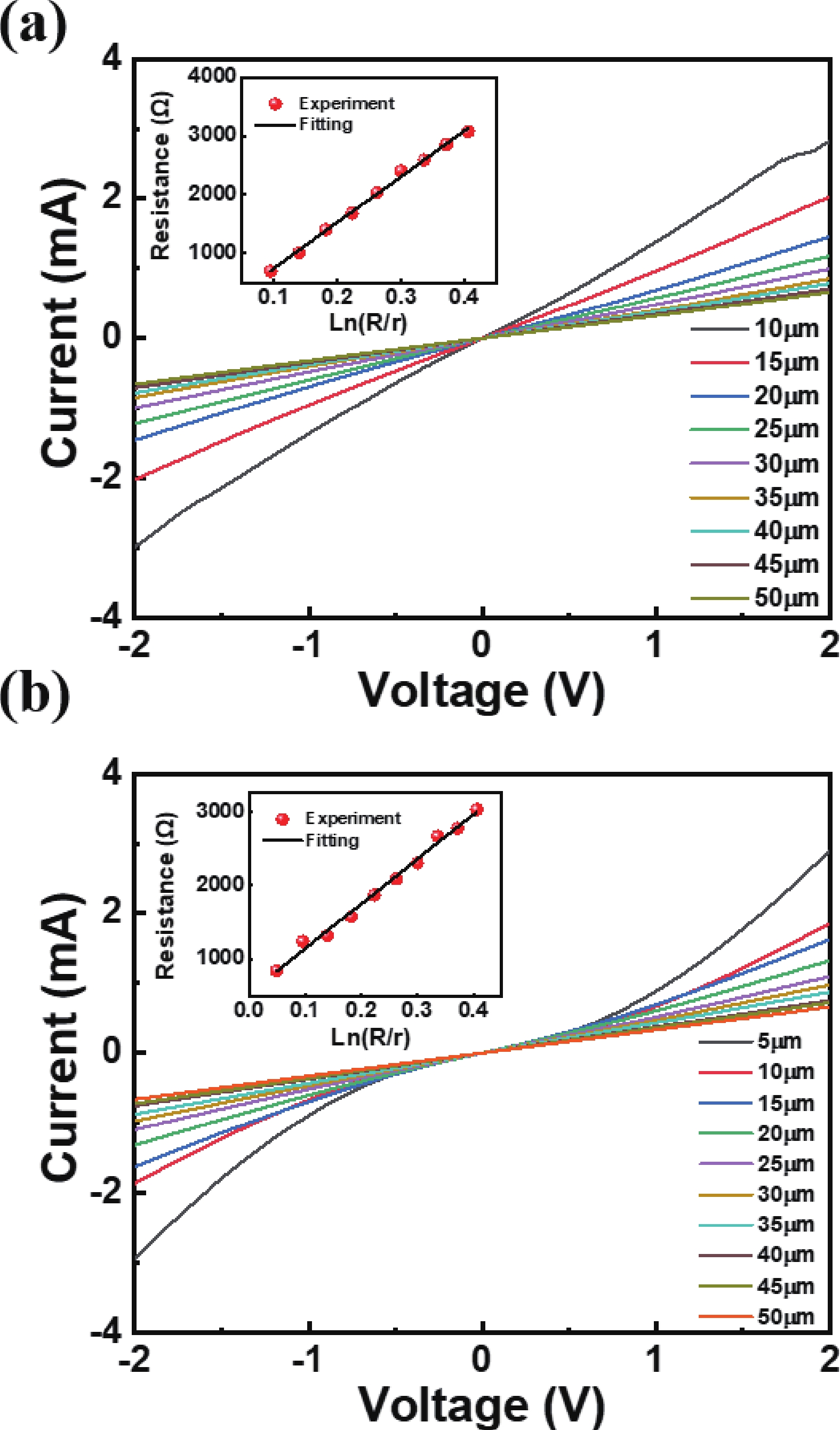
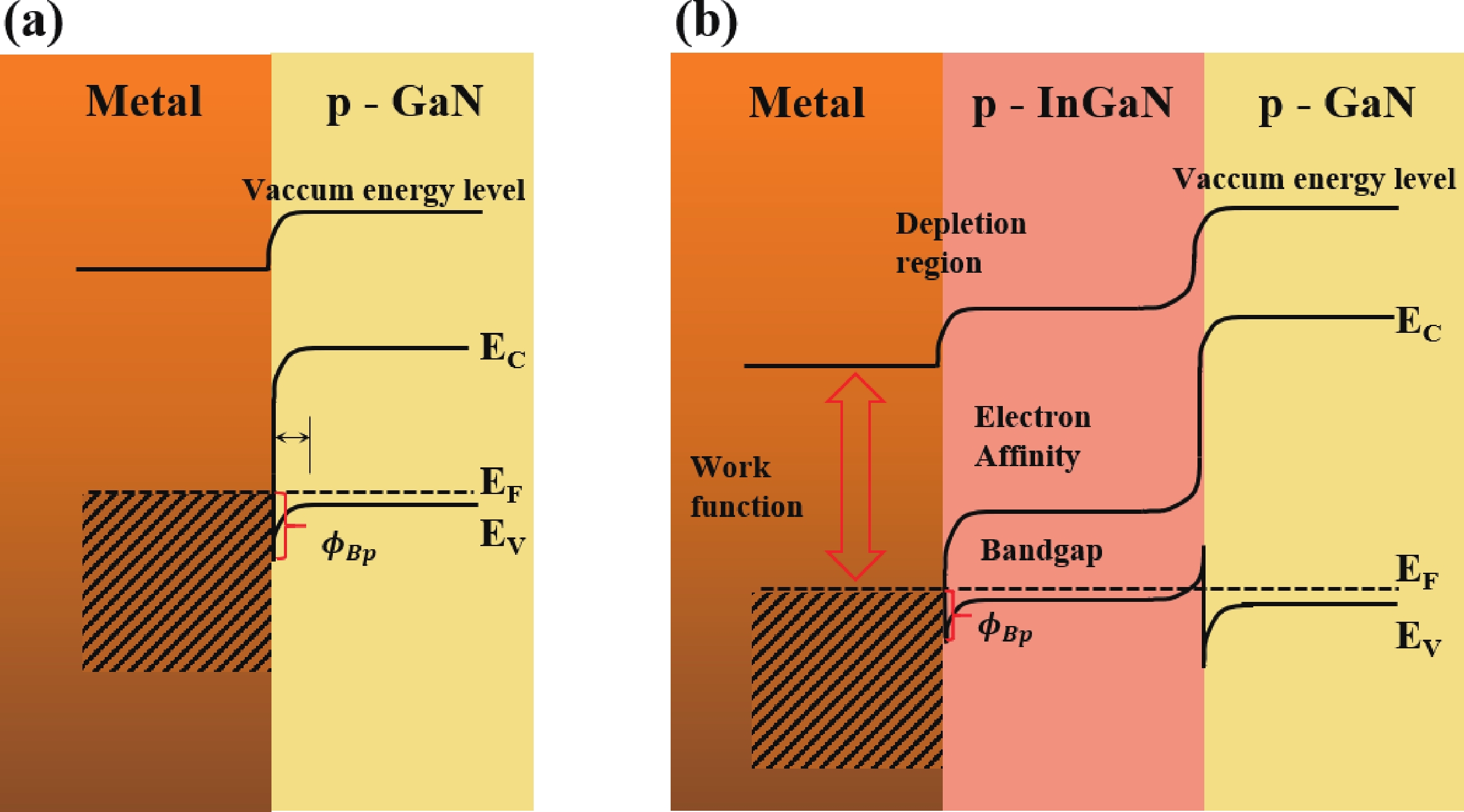
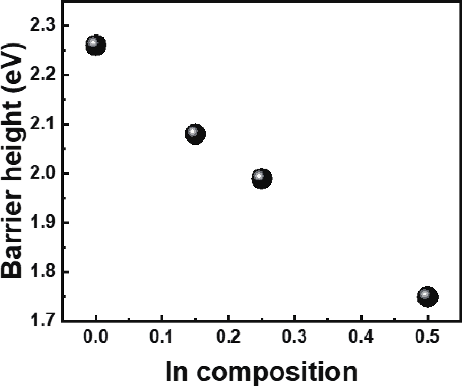
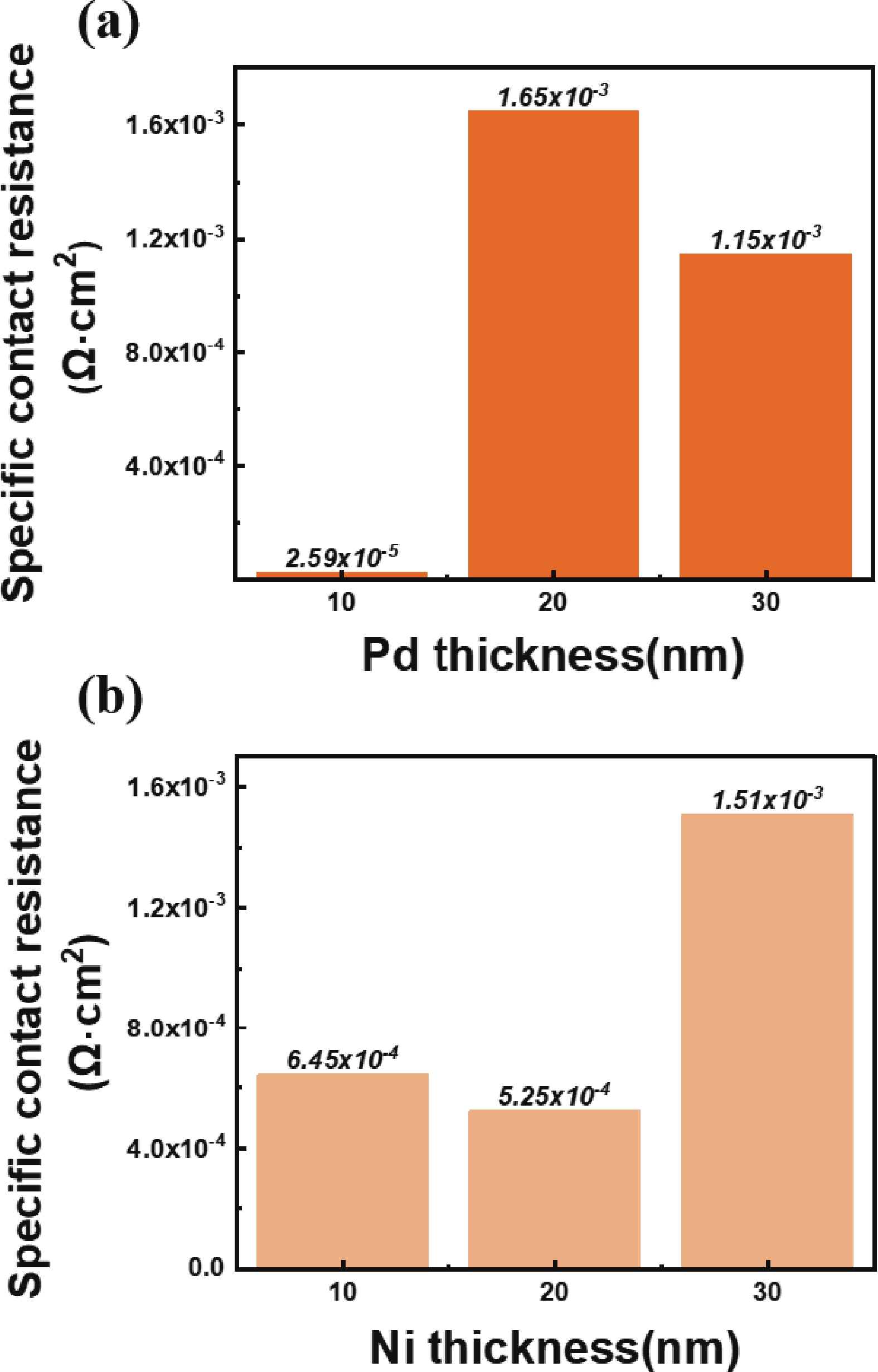
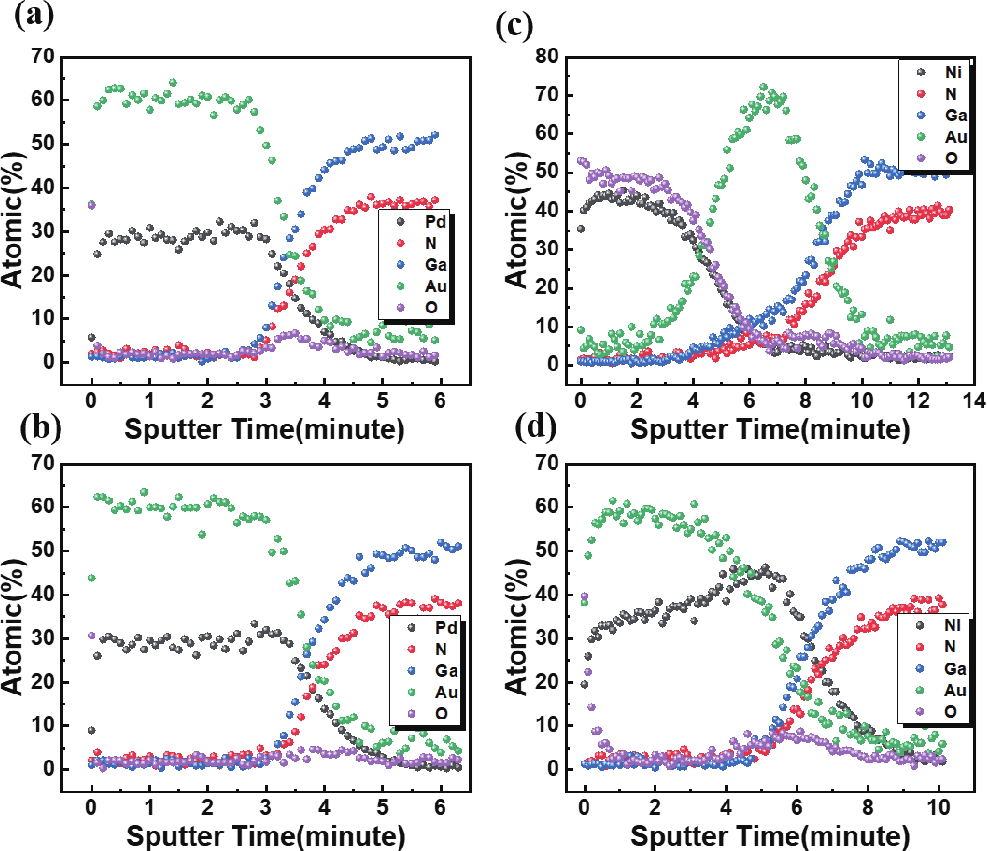
| [1] |
Adachi M. InGaN based green laser diodes on semipolar GaN substrate. Jpn J Appl Phys, 2014, 53, 100207 doi: 10.7567/JJAP.53.100207 |
| [2] |
Shen C, Ng T K, Leonard J T, et al. High-modulation-efficiency, integrated waveguide modulator–laser diode at 448 nm. ACS Photonics, 2016, 3, 262 doi: 10.1021/acsphotonics.5b00599 |
| [3] |
Shen C, Lee C M, Stegenburgs E, et al. Semipolar Ⅲ–nitride quantum well waveguide photodetector integrated with laser diode for on-chip photonic system. Appl Phys Express, 2017, 10, 042201 doi: 10.7567/APEX.10.042201 |
| [4] |
Shen C, Ng T K, Lee C M, et al. Semipolar InGaN quantum-well laser diode with integrated amplifier for visible light communications. Opt Express, 2018, 26, A219 doi: 10.1364/OE.26.00A219 |
| [5] |
Chi N, Haas H, Kavehrad M, et al. Visible light communications: Demand factors, benefits and opportunities (Guest Editorial). IEEE Wirel Commun, 2015, 22, 5 doi: 10.1109/mwc.2015.7096278 |
| [6] |
Huang Y F, Chi Y C, Kao H Y, et al. Blue laser diode based free-space optical data transmission elevated to 18 Gbps over 16 m. Sci Rep, 2017, 7, 10478 doi: 10.1038/s41598-017-10289-y |
| [7] |
Koide Y, Maeda T, Kawakami T, et al. Effects of annealing in an oxygen ambient on electrical properties of ohmic contacts to p-type GaN. J Electron Mater, 1999, 28, 341 doi: 10.1007/s11664-999-0037-7 |
| [8] |
Jang J S, Park S J, Seong T Y. Metallization scheme for highly low-resistance, transparent, and thermally stable Ohmic contacts to p-GaN. Appl Phys Lett, 2000, 76, 2898 doi: 10.1063/1.126510 |
| [9] |
|
| [10] |
Chen J L, Brewer W D. Ohmic contacts on p-GaN. Adv Electron Mater, 2015, 1, 1500113 doi: 10.1002/aelm.201500113 |
| [11] |
Lu S, Deki M, Wang J, et al. Ohmic contact on low-doping-density p-type GaN with nitrogen-annealed Mg. Appl Phys Lett, 2021, 119, 242104 doi: 10.1063/5.0076764 |
| [12] |
Foresi J S, Moustakas T D. Metal contacts to gallium nitride. Appl Phys Lett, 1993, 62, 2859 doi: 10.1063/1.109207 |
| [13] |
Lin M E, Ma Z, Huang F Y, et al. Low resistance ohmic contacts on wide band-gap GaN. Appl Phys Lett, 1994, 64, 1003 doi: 10.1063/1.111961 |
| [14] |
Fan Z F, Mohammad S N, Kim W, et al. Very low resistance multilayer Ohmic contact to n-GaN. Appl Phys Lett, 1996, 68, 1672 doi: 10.1063/1.115901 |
| [15] |
Chen L C, Chen F R, Kai J J, et al. Microstructural investigation of oxidized Ni/Au ohmic contact to p-type GaN. J Appl Phys, 1999, 86, 3826 doi: 10.1063/1.371294 |
| [16] |
Chen L C, Ho J K, Jong C S, et al. Oxidized Ni/Pt and Ni/Au ohmic contacts to p-type GaN. Appl Phys Lett, 2000, 76, 3703 doi: 10.1063/1.126755 |
| [17] |
Oh M S, Hwang D K, Lim J H, et al. Low resistance nonalloyed Ni∕Au Ohmic contacts to p-GaN irradiated by KrF excimer laser. Appl Phys Lett, 2006, 89, 042107 doi: 10.1063/1.2236656 |
| [18] |
Greco G, Prystawko P, Leszczyński M, et al. Electro-structural evolution and Schottky barrier height in annealed Au/Ni contacts onto p-GaN. J Appl Phys, 2011, 110, 123703 doi: 10.1063/1.3669407 |
| [19] |
King D J, Zhang L, Ramer J C, et al. Temperature behavior of Pt/Au ohmic contacts to p-GaN. MRS Online Proc Libr, 1997, 468, 421 doi: 10.1557/PROC-468-421 |
| [20] |
Trexler J T, Pearton S J, Holloway P H, et al. Comparison of Ni/Au, Pd/Au, and Cr/Au metallizations for ohmic contacts to p-GaN. MRS Online Proc Libr, 1996, 449, 1091 doi: 10.1557/PROC-449-1091 |
| [21] |
Kim T, Khim J, Chae S, et al. Low resistance contacts to P-type GaN. MRS Online Proc Libr, 1997, 468, 427 doi: 10.1557/PROC-468-427 |
| [22] |
Kim J K, Lee J L, Lee J W, et al. Low resistance Pd/Au ohmic contacts to p-type GaN using surface treatment. Appl Phys Lett, 1998, 73, 2953 doi: 10.1063/1.122641 |
| [23] |
Jang J S, Chang I S, Kim H K, et al. Low-resistance Pt/Ni/Au ohmic contacts to p-type GaN. Appl Phys Lett, 1999, 74, 70 doi: 10.1063/1.123954 |
| [24] |
Zhou L, Lanford W, Ping A T, et al. Low resistance Ti/Pt/Au ohmic contacts to p-type GaN. Appl Phys Lett, 2000, 76, 3451 doi: 10.1063/1.126674 |
| [25] |
Durbha A, Pearton S J, Abernathy C R, et al. Microstructural stability of ohmic contacts to In xGa 1–i>xN. J Vac Sci Technol B Microelectron Nanometer Struct Process Meas Phenom, 1996, 14, 2582 doi: 10.1116/1.588771 |
| [26] |
|
| [27] |
Wang W J, Xie W Z, Deng Z J, et al. Performance improvement of GaN based laser diode using Pd/Ni/Au metallization ohmic contact. Coatings, 2019, 9, 291 doi: 10.3390/coatings9050291 |
| [28] |
Moses P G, Miao M S, Yan Q M, et al. Hybrid functional investigations of band gaps and band alignments for AlN, GaN, InN, and InGaN. J Chem Phys, 2011, 134, 084703 doi: 10.1063/1.3548872 |
| [29] |
Lee J L, Kim J K, Lee J W, et al. Transparent Pt ohmic contact on p-type GaN with low resistivity using (NH4)2Sx treatment, electrochem. Solid-State Lett, 1999, 3, 53
|
| [30] |
Lee J L, Kim J K. Ohmic contact formation mechanism of Pd nonalloyed contacts on p-type GaN. J Electrochem Soc, 2000, 147, 2297 doi: 10.1149/1.1393524 |
| [31] |
Ho J K, Jong C S, Chiu C C, et al. Low-resistance ohmic contacts to p-type GaN achieved by the oxidation of Ni/Au films. J Appl Phys, 1999, 86, 4491 doi: 10.1063/1.371392 |
| [32] |
Oh M S, Kim S H, Hwang D K, et al. Formation of low resistance nonalloyed Ti∕Au ohmic contacts to n-type ZnO by KrF excimer laser irradiation. Electrochem Solid-State Lett, 2005, 8, G317 doi: 10.1149/1.2056447 |


 Junfei Wang received his PhD at the School of Information Science and Technology, Fudan University, specializing in electronic information. He earned his master's degree from the Institute of Semiconductors at the Chinese Academy of Sciences and his bachelor's degree from Shandong University. Wang has extensive experience in GaN-based super luminescence diodes (SLDs) and laser diodes (LDs). His work includes the design and fabrication of nitride light emitters, along with their applications in visible light communication systems.
 Chao Shen is currently a professor at the School of Information Science and Technology, Fudan University. He has published 100+ peer-reviewed publications in the fields of Ⅲ-Nitride optoelectronics devices, semiconductor lasers, superluminescent diodes, photonics integrated circuits, visible light communications (VLC), and underwater wireless optical communications (UWOC). Dr. Shen has served as a TPC member and invited speaker in many IEEE, Optica, and SPIE conferences, and is the associated editor of IEEE Photonics Journal. Dr. Shen received his PhD in Electrical Engineering from KAUST and his BSc in Materials Physics from Fudan University.
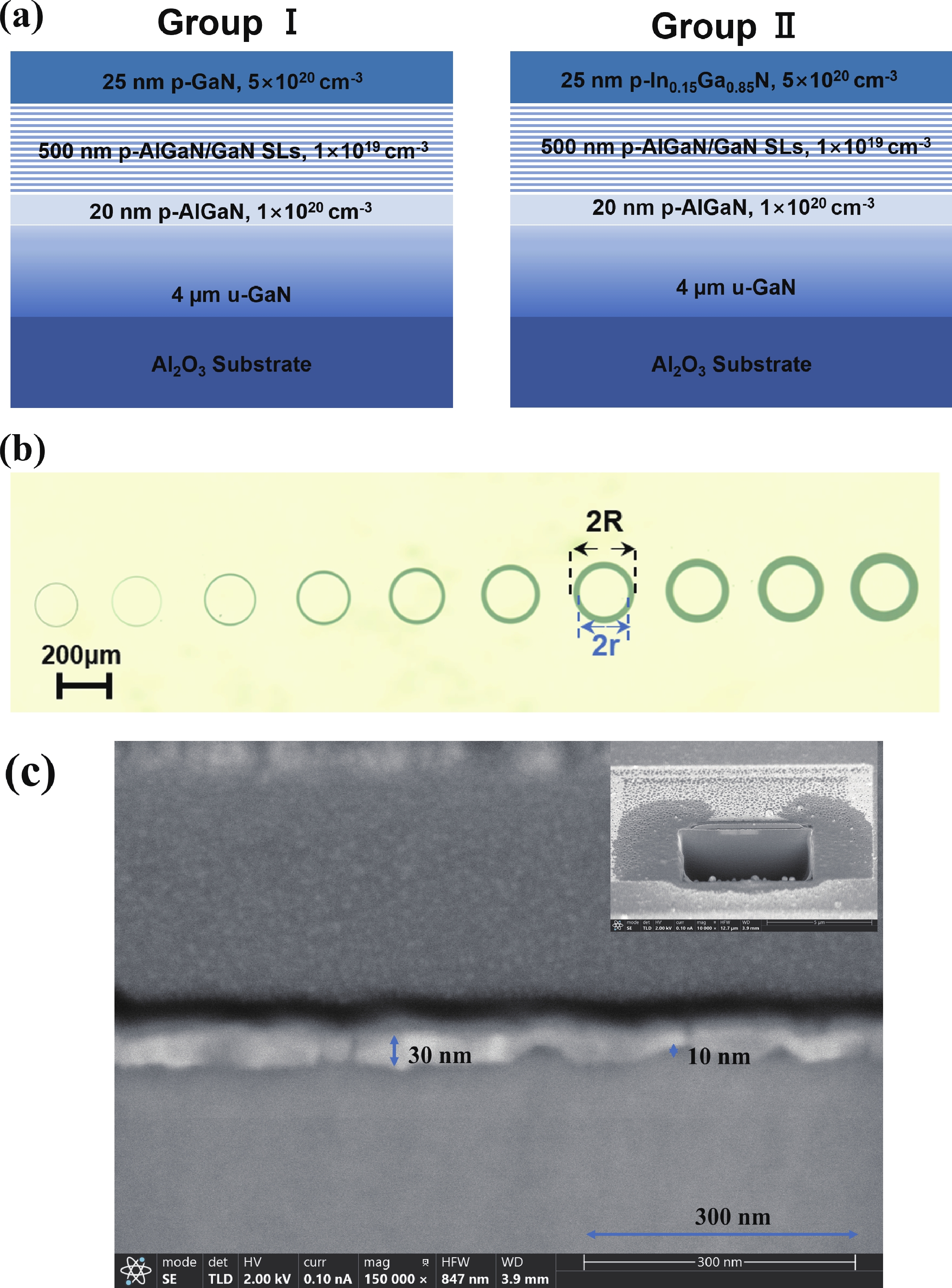
 DownLoad: