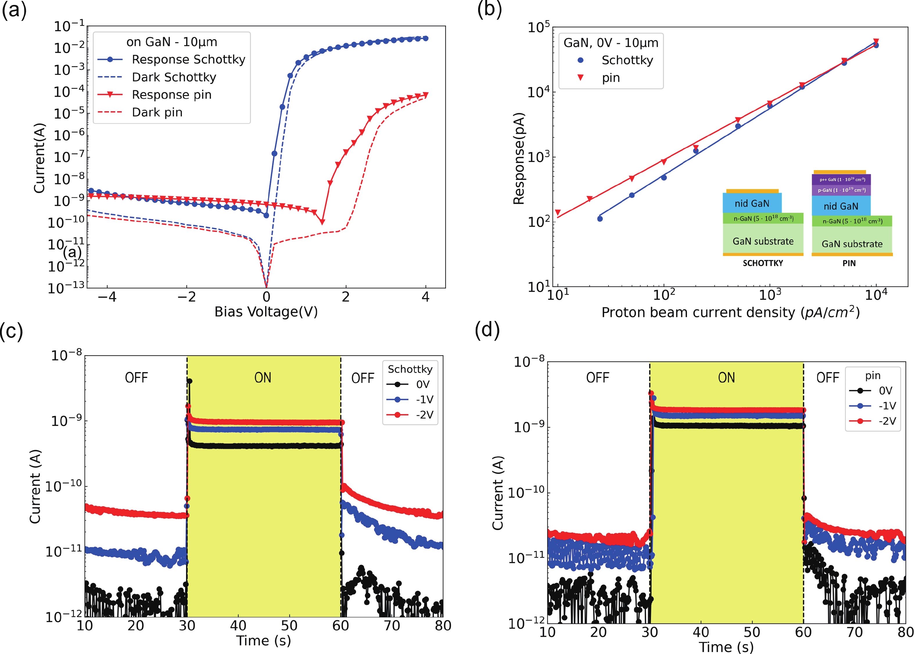
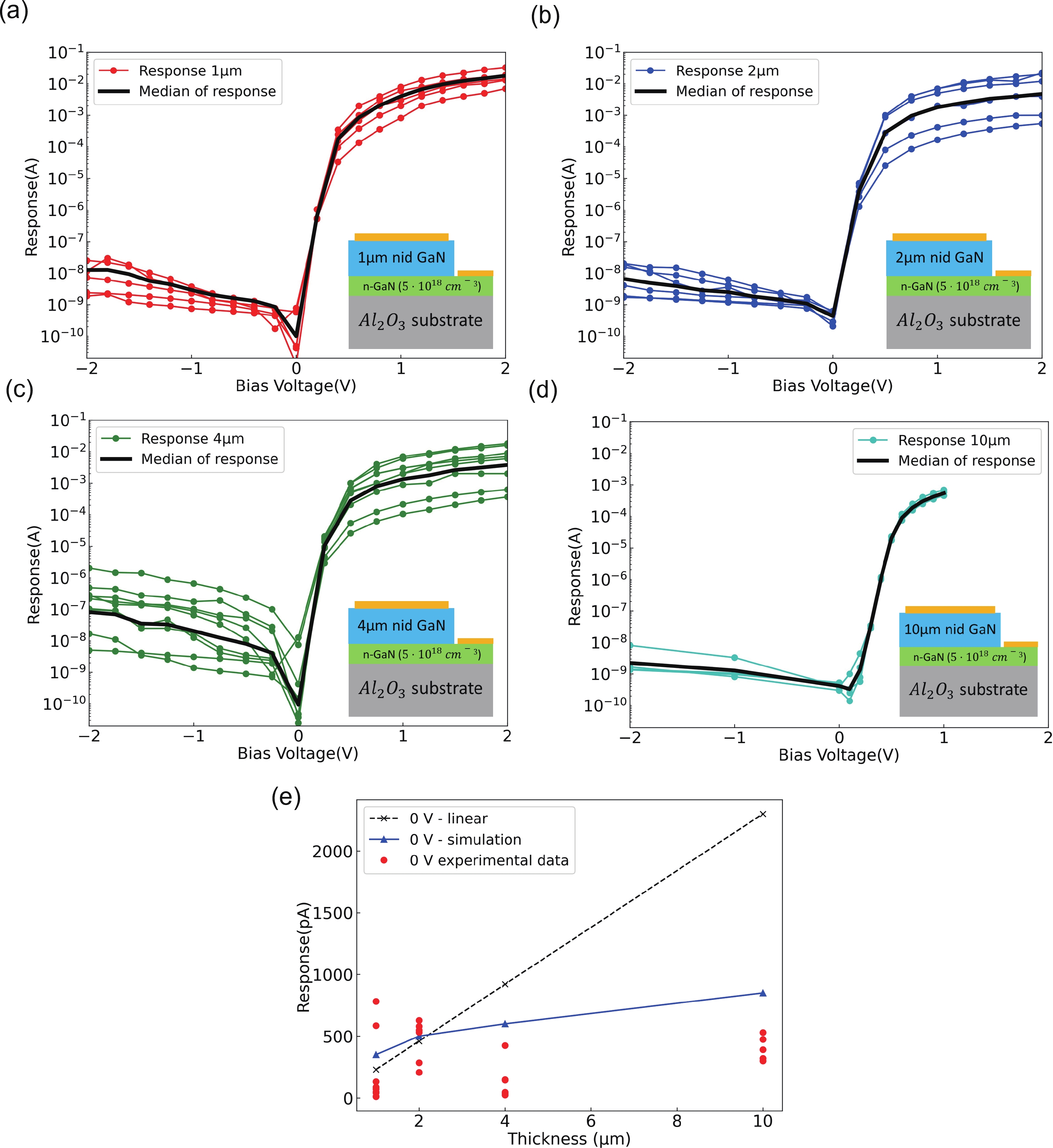
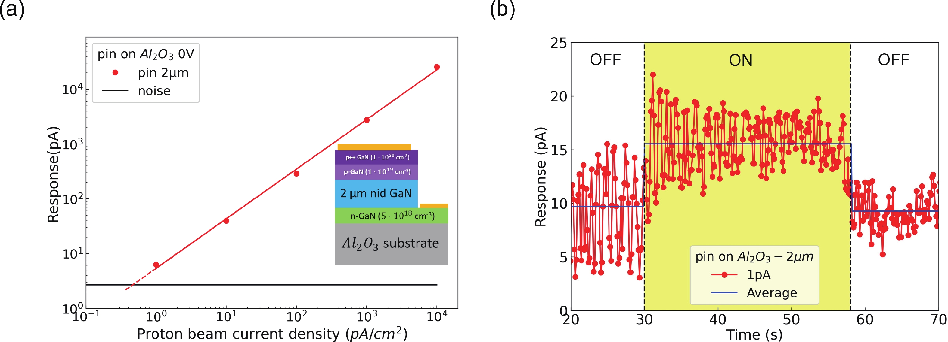
| [1] |
Wilson R R. Radiological use of fast protons. Radiology, 1946, 47(5), 487 doi: 10.1148/47.5.487 |
| [2] |
Mohan R. A review of proton therapy-current status and future directions. Precis Radiat Oncol, 2022, 6(2), 164 doi: 10.1002/pro6.1149 |
| [3] |
Cirrone G A P, Cuttone G, Lojacono et al. A 62-MeV proton beam for the treatment of ocular melanoma at Laboratori Nazionali del Sud-INFN. IEEE Trans Nucl Sci, 2004, 51(3), 860 doi: 10.1109/TNS.2004.829535 |
| [4] |
Arjomandy B, Sahoo N, Ding X, et al. Use of a two-dimensional ionization chamber array for proton therapy beam quality assurance. Med Phys, 2008, 35(9), 3889 doi: 10.1118/1.2963990 |
| [5] |
Taylor J T, Waltham C, Price T, et al. A new silicon tracker for proton imaging and dosimetry. Nucl Instrum Methods Phys Res Sect Accel Spectrometers Detect Assoc Equip, 2016, 831, 362 doi: 10.1016/j.nima.2016.02.013 |
| [6] |
Esposito M, Waltham C, Taylor J T, et al. PRaVDA: The first solid-state system for proton computed tomography. Phys Med, 2018, 55, 149 doi: 10.1016/j.ejmp.2018.10.020 |
| [7] |
Russo S, Mirandola A, Molinelli S, et al. Characterization of a commercial scintillation detector for 2-D dosimetry in scanned proton and carbon ion beams. Phys Med, 2017, 34, 48 doi: 10.1016/j.ejmp.2017.01.011 |
| [8] |
De Napoli M. SiC detectors: A review on the use of silicon carbide as radiation detection material. Front Phys, 2022, 10, doi: 10.3389/fphy.2022.898833 |
| [9] |
Milluzzo G, De Napoli M, Di Martino F, et al. Comprehensive dosimetric characterization of novel silicon carbide detectors with UHDR electron beams for FLASH radiotherapy. Med Phys, 2024, 51, 6390 doi: 10.1002/mp.17172 |
| [10] |
Wyrsch N, Antognini L, Ballif C, et al. Amorphous silicon detectors for proton beam monitoring in FLASH radiotherapy. Radiat Meas, 2024, 177, 107230 doi: 10.1016/j.radmeas.2024.107230 |
| [11] |
Levin DS, Friedman PS, Ferretti C, et al. A prototype scintillator real-time beam monitor for ultra-high dose rate radiotherapy. Med Phys, 2024, 2905 doi: 10.1002/mp.17018 |
| [12] |
Floriduz A, Devine J D. Modelling of proton irradiated GaN-based high-power white light-emitting diodes. Jpn J Appl Phys, 2018, 57, 080304 doi: 10.7567/JJAP.57.080304 |
| [13] |
Harper R S, Buttar C M, Allport P P, et al. Evolution of silicon microstrip detector currents during proton irradiation at the CERN PS. Nucl Instrum Methods Phys Res Sect Accel Spectrometers Detect Assoc Equip, 2002, 479(2/3), 548 doi: 10.1016/S0168-9002(01)00945-7 |
| [14] |
Pearton S J, Deist R, Ren F, et al. Review of radiation damage in GaN-based materials and devices. J Vac Sci Technol Vac Surf Films, 2013, 31, 050801 doi: 10.1116/1.4799504 |
| [15] |
Logan J V, Woller K B, Webster P T, et al. Open volume defect accumulation with irradiation in GaN, GaP, InAs, InP, Si, ZnO, and MgO. J Appl Phys, 2023, 134, 225701 doi: 10.1063/5.0147324 |
| [16] |
Alaie Z, Mohammad Nejad S, Yousefi M H. Recent advances in ultraviolet photodetectors. Mater Sci Semicond Process, 2015, 29, 16 doi: 10.1016/j.mssp.2014.02.054 |
| [17] |
Sandupatla A, Arulkumaran S, Ranjan K, et al. Low voltage high-energy α-particle detectors by GaN-on-GaN schottky diodes with record-high charge collection efficiency. Sensors, 2019, 19, 5107 doi: 10.3390/s19235107 |
| [18] |
Zhou C, Melton A G, Burgett E, et al. Neutron detection performance of gallium nitride based semiconductors. Sci Rep, 2019, 9, 17551 doi: 10.1038/s41598-019-53664-7 |
| [19] |
Duboz J Y, Zucchi J, Frayssinet E, et al. GaN Schottky diodes for proton beam monitoring. Biomed Phys Eng Express, 2019, 5, 025015 doi: 10.1088/2057-1976/aaf9b4 |
| [20] |
Arjomandy B, Taylor P, Ainsley C, et al. AAPM task group 224: Comprehensive proton therapy machine quality assurance. Med Phys, 2019, 46 doi: 10.1002/mp.13622 |
| [21] |
William Steward V, Koehler A M. Proton radiography in the diagnosis of breast carcinoma. Radiology, 1974, 110, 217 doi: 10.1148/110.1.217 |
| [22] |
Poludniowski G, Allinson N M, Evans P M. Proton radiography and tomography with application to proton therapy. Br J Radiol, 2015, 88, 20150134 doi: 10.1259/bjr.20150134 |
| [23] |
Lane S A, Slater J M, Yang G Y. Image-guided proton therapy: A comprehensive review. Cancers, 2023, 15, 2555 doi: 10.3390/cancers15092555 |
| [24] |
Uwe Schneider, Eros Pedroni. Proton radiography as a tool for quality control in proton therapy. Med Phys, 1995, 22, 353 doi: 10.1118/1.597470 |
| [25] |
Duboz J Y, Zucchi J, Frayssinet E, et al. Proton energy loss in GaN. Phys Status Solidi B, 2021, 258, 2100167 doi: 10.1002/pssb.202100167 |
| [26] |
Gian W, Skowronski M, Rohrer G S. Structural defects and their relationship to nucleation of gan thin films. MRS Proc, 1996, 423(1), 475 doi: 10.1557/PROC-423-475 |
| [27] |
Roder C, Einfeldt S, Figge S, et al. Stress and wafer bending of a-plane GaN layers on r-plane sapphire substrates. J Appl Phys, 2006, 100(10), 103511 doi: 10.1063/1.2386940 |


 Matilde Siviero received her bachelor degree in Physics at University of Padova (Italy) in 2020 and her master’s degree in Materials Science in 2022 at the same University. At the moment, she is a doctoral student for Université Côte d’Azur (France) at CRHEA-CNRS under the supervision of Prof. Jean-Yves Duboz and Andreas Wieck, in a joint PhD with University of Bochum (Germany). Her research focuses on GaN-based devices fabrication and device characterization.
 Maxime Hugues received the Ph.D. degree in Physics from Nice-Sophia Antipolis University (France) in 2007. He worked on dilute nitride and quantum dots for long-wavelength lasers at CRHEA-CNRS. In 2007, he joined the Department of Electronic and Electrical Engineering, University of Sheffield (U.K.) where he was involved in the Ⅲ–Ⅴnanostructures growth by molecular beam epitaxy. Since 2013 he is a CNRS permanent researcher at CRHEA where he took the responsibility of the SEMI team in 2023, developing electronic devices and MEMS. He is the author/coauthor of more than 110 publications and gave over 40 oral presentations at international conferences.
 Eric Frayssinet obtained his doctoral degree in physics of condensed matter in 2000 at the University of Sciences and Techniques of Languedoc (Montpellier). He is currently a Research Engineer at CNRS-CRHEA. His main research topic concerns the epitaxy of element Ⅲ nitrides on various substrates (sapphire, silicon, GaN, SiC, etc.).
 Shirley Prado de la Cruz was born in Lima, Peru in 1993. She received her bachelor’s degree in Physics from University of Toulouse–Paul Sabatier, France in 2018 and her master’s degree in Nanoscience and Nanotechnologies from University Paris-Saclay, France in 2020. During her studies she worked on InP devices for telecommunication. She has also worked on GaN nanowires for flexible LEDs and GaN devices for protontherapy. She is currently a doctoral student at Telecom Paris working on Photonic Integrated Circuits on InP for 5G access network.
 Sebastien Chenot graduated with a DESS TAP (Techniqus et Applications de la Physique) from the University of Grenoble Alpes in 2001. He has been responsible for the clean room at CRHEA (Centre de Recherche sur l'Hétéroépitaxie et ses Applications) since 2004. He develops technological processes for various CREHA research projects.
 Jean-Yves Duboz is a specialized in electronic and optical properties of semiconductors and related heterostructures, in particular Ⅲ–Ⅴ semiconductors. His field of expertise also includes the physics of devices, in particular optoelectronic devices. He studied intersubband transitions in GaAs based materials and developed QWIP detectors. He studied diluted nitrides and quantum dot structures. Then he developed UV detectors based on AlGaN. He developed GaN based lasers and nanophotonic devices. He owns 10 patents and more than 150 publications.
 DownLoad: