J. Semicond. >  Just Accepted

ARTICLES

A photolithography-compatible method for transferring full-device constituents on silicon substrate

Zunxian Lv1, Shun Zhang1, Mingjian Yang1, Xinsheng Wang1, Zhaochao Liu1, Yameng Hou1, 2, Jiabiao Chen1, , Moyuan Cao1, Feng Luo1 and Jinxiong Wu1,

+ Author Affiliations

 Corresponding author: Jiabiao Chen, jbchen@nankai.edu.cn; Jinxiong Wu, jxwu@nankai.edu.cn

DOI: 10.1088/1674-4926/26080030CSTR: 32376.14.1674-4926.26080030

PDF

Turn off MathJax

Abstract: Transfer printing offers a promising route to integrate pre-fabricated device components with two-dimensional (2D) semiconductors, yet most existing approaches rely on deliberately deposited buffer layers or specialized substrates, adding complexity and limiting compatibility with standard silicon fabrication. Here, we report a simple and photolithography-compatible strategy that leverages the ultrathin lift-off-resist (LOR) residue, which naturally retains on a commercial silicon substrate after standard photolithography, as a sacrificial release layer. This ~2 nm-thick residue allows selective water intercalation at the LOR/Si interface, enabling damage-free delamination of various pre-fabricated metal electrodes, high-κ metal gate (HKMG) stacks, and even entire device stacks directly from the Si substrate. Besides, the top-gated MoS2 transistor was fabricated by one-step laminating the full-device stack onto the MoS2 flake, yielding a clean van der Waals interface, small subthreshold swing and negligible gate hysteresis. Our method eliminates the need for additional sacrificial layer deposition or specialized handling substrates, offering a facile method to transfer full-device constituents on industry-compatible Si substrate.

Keywords: transfer printing, photolithography, LOR residue, full-device stacks, commercial silicon substrate


[1]
Liu Y, Duan X D, Shin H J, et al. Promises and prospects of two-dimensional transistors. Nature, 2021, 591(7848): 43 doi: 10.1038/s41586-021-03339-z
[2]
Ma L K, Wang Y L, Liu Y. Van der Waals contact for two-dimensional transition metal dichalcogenides. Chem Rev, 2024, 124(5): 2583 doi: 10.1021/acs.chemrev.3c00697
[3]
Das S, Sebastian A, Pop E, et al. Transistors based on two-dimensional materials for future integrated circuits. Nat Electron, 2021, 4(11): 786 doi: 10.1038/s41928-021-00670-1
[4]
Liu C S, Chen H W, Wang S Y, et al. Two-dimensional materials for next-generation computing technologies. Nat Nanotechnol, 2020, 15(7): 545 doi: 10.1038/s41565-020-0724-3
[5]
Duan X D, Wang C, Pan A L, et al. Two-dimensional transition metal dichalcogenides as atomically thin semiconductors: Opportunities and challenges. Chem Soc Rev, 2015, 44(24): 8859 doi: 10.1039/C5CS00507H
[6]
Chen J B, Liu Z C, Dong X Y, et al. Vertically grown ultrathin Bi2SiO5 as high-κ single-crystalline gate dielectric. Nat Commun, 2023, 14(1): 4406 doi: 10.1038/s41467-023-40123-1
[7]
Wang Y, Sarkar S, Yan H, et al. Critical challenges in the development of electronics based on two-dimensional transition metal dichalcogenides. Nat Electron, 2024, 7(8): 638 doi: 10.1038/s41928-024-01210-3
[8]
Wang S Y, Liu X X, Xu M S, et al. Two-dimensional devices and integration towards the silicon lines. Nat Mater, 2022, 21(11): 1225 doi: 10.1038/s41563-022-01383-2
[9]
Poddar P K, Zhong Y, Mannix A J, et al. Resist-free lithography for monolayer transition metal dichalcogenides. Nano Lett, 2022, 22(2): 726 doi: 10.1021/acs.nanolett.1c04081
[10]
Nakatani M, Fukamachi S, Solís-Fernández P, et al. Ready-to-transfer two-dimensional materials using tunable adhesive force tapes. Nat Electron, 2024, 7(2): 119 doi: 10.1038/s41928-024-01121-3
[11]
Wang Y, Kim J C, Li Y, et al. P-type electrical contacts for 2D transition-metal dichalcogenides. Nature, 2022, 610(7930): 61 doi: 10.1038/s41586-022-05134-w
[12]
Shen P C, Su C, Lin Y X, et al. Ultralow contact resistance between semimetal and monolayer semiconductors. Nature, 2021, 593(7858): 211 doi: 10.1038/s41586-021-03472-9
[13]
Yang Z L, Huang B C, Lin Y K, et al. Directly probing the carrier transfer length in 2D-material transistors. Nature, 2026, 655(8122): 350 doi: 10.1038/s41586-026-10707-0
[14]
Zhang L, Liu Z C, Ai W, et al. Vertically grown metal nanosheets integrated with atomic-layer-deposited dielectrics for transistors with subnanometre capacitance-equivalent thicknesses. Nat Electron, 2024, 7(8): 662 doi: 10.1038/s41928-024-01202-3
[15]
Xu Y S, Liu T, Liu K L, et al. Scalable integration of hybrid high-κ dielectric materials on two-dimensional semiconductors. Nat Mater, 2023, 22(9): 1078 doi: 10.1038/s41563-023-01626-w
[16]
Li W S, Zhou J, Cai S H, et al. Uniform and ultrathin High-κ gate dielectrics for two-dimensional electronic devices. Nat Electron, 2019, 2(12): 563 doi: 10.1038/s41928-019-0334-y
[17]
Sim K, Chen S, Li Z W, et al. Three-dimensional curvy electronics created using conformal additive stamp printing. Nat Electron, 2019, 2(10): 471 doi: 10.1038/s41928-019-0304-4
[18]
Meitl M A, Zhu Z T, Kumar V, et al. Transfer printing by kinetic control of adhesion to an elastomeric stamp. Nat Mater, 2005, 5(1): 33
[19]
Shin Y, Hong S, Hur Y C, et al. Damage-free dry transfer method using stress engineering for high-performance flexible two- and three-dimensional electronics. Nat Mater, 2024, 23(10): 141
[20]
Liu G Y, Tian Z A, Yang Z Y, et al. Graphene-assisted metal transfer printing for wafer-scale integration of metal electrodes and two-dimensional materials. Nat Electron, 2022, 5(5): 275 doi: 10.1038/s41928-022-00764-4
[21]
Liu Y, Guo J, Zhu E B, et al. Approaching the Schottky–Mott limit in van der Waals metal–semiconductor junctions. Nature, 2018, 557(7707): 696 doi: 10.1038/s41586-018-0129-8
[22]
Yang X D, Li J, Song R, et al. Highly reproducible van der Waals integration of two-dimensional electronics on the wafer scale. Nat Nanotechnol, 2023, 18(5): 471 doi: 10.1038/s41565-023-01342-1
[23]
Zeng D B, Zhang Z Y, Xue Z Y, et al. Single-crystalline metal-oxide dielectrics for top-gate 2D transistors. Nature, 2024, 632(8026): 788 doi: 10.1038/s41586-024-07786-2
[24]
Qi D Y, Li P, Ou H H, et al. Graphene-enhanced metal transfer printing for strong van der Waals contacts between 3D metals and 2D semiconductors. Adv Funct Mater, 2023, 33(27): 2301704 doi: 10.1002/adfm.202301704
[25]
Wu Y H, Xin Z Q, Zhang Z B, et al. All-transfer electrode interface engineering toward harsh-environment-resistant MoS2 field-effect transistors. Adv Mater, 2023, 35(18): 2210735 doi: 10.1002/adma.202210735
[26]
Wang L Y, Wang P Q, Huang J, et al. A general one-step plug-and-probe approach to top-gated transistors for rapidly probing delicate electronic materials. Nat Nanotechnol, 2022, 17(11): 1206 doi: 10.1038/s41565-022-01221-1
[27]
Kwon G, Choi Y H, Lee H, et al. Interaction- and defect-free van der waals contacts between metals and two-dimensional semiconductors. Nat Electron, 2022, 5(4): 241 doi: 10.1038/s41928-022-00746-6
[28]
Hong M Y, Zhang X K, Geng Y, et al. Universal transfer of full-class metal electrodes for barrier-free two-dimensional semiconductor contacts. InfoMat, 2023, 6(1): e12491
[29]
Kong L G, Wu R X, Chen Y, et al. Wafer-scale and universal van der Waals metal semiconductor contact. Nat Commun, 2023, 14(1): 1014 doi: 10.1038/s41467-023-36715-6
[30]
Lu Z Y, Chen Y, Dang W Q, et al. Wafer-scale high-κ dielectrics for two-dimensional circuits via van der Waals integration. Nat Commun, 2023, 14(1): 2340 doi: 10.1038/s41467-023-37887-x
[31]
Xing K J, McEwen D, Yin Y F, et al. Pick-and-place transfer of arbitrary-metal electrodes for van der Waals device fabrication. ACS Nano, 2025, 19(3): 3579 doi: 10.1021/acsnano.4c13592
[32]
Zhang X D, Huang C X, Li Z Y, et al. Reliable wafer-scale integration of two-dimensional materials and metal electrodes with van der Waals contacts. Nat Commun, 2024, 15(1): 4619 doi: 10.1038/s41467-024-49058-7
[33]
Yan Y J, Yan T, Wang F, et al. Cmos-compatible fabrication of 2D semiconductor-based cfets via High-κ dielectric van der Waals encapsulation. Nano Lett, 2025, 25(15): 6125 doi: 10.1021/acs.nanolett.5c00220
[34]
He Y Y, Lv Z X, Liu Z C, et al. Sacrifice-layer-free transfer of wafer-scale atomic-layer-deposited dielectrics and full-device stacks for two-dimensional electronics. Nat Commun, 2025, 16(1): 5904 doi: 10.1038/s41467-025-60864-5
[35]
Jiang J F, Wu P, Liu Y F, et al. Towards fab-compatible two-dimensional electronics. Nat Rev Electr Eng, 2025, 2(1): 6 doi: 10.1038/s44287-024-00125-7
[36]
Hwang E, Hong H, Lee Y, et al. Van der Waals materials for energy-efficient electronic devices. Nature Reviews Materials, 2026, 11(4): 308 doi: 10.1038/s41578-025-00886-z
[37]
Kim K S, Kwon J, Ryu H, et al. The future of two-dimensional semiconductors beyond Moore’s law. Nat Nanotechnol, 2024, 19(7): 895 doi: 10.1038/s41565-024-01695-1
[38]
Li Y F, Liu S Q, Zheng H, et al. From planar to 3D: The evolution of complementary field-effect transistor for next-generation semiconductor nodes. Adv Mater, 2026, 38(32): e73226 doi: 10.1002/adma.73226
[39]
Zeng S F, Liu C S, Huang X H, et al. An application-specific image processing array based on WSe2 transistors with electrically switchable logic functions. Nat Commun, 2022, 13(1): 56 doi: 10.1038/s41467-021-27644-3
[40]
Xu M S, Wang Y W, Liu J W, et al. Progress on the program of Si-compatible two-dimensional semiconductor materials and devices. Sci China Inf Sci, 2024, 67(6): 160401 doi: 10.1007/s11432-024-3986-8
[41]
Xia X X, Yang H F, Sun Y M, et al. Fabrication of terahertz metamaterials using S1813/LOR stack by lift-off. Microelectron Eng, 2008, 85(5): 1433
[42]
Chen Y F, Peng K W, Cui, Z. A lift-off process for high resolution patterns using pmma/LOR resist stack. Microelectron Eng, 2004, 73: 278
[43]
Preiss E M, Krauss A, Seidel H. Sputtered Pt electrode structures with smoothly tapered edges by bi-layer resist lift-off. Thin Solid Films, 2015, 597: 158 doi: 10.1016/j.tsf.2015.11.026
[44]
Lyytinen J, Berdova M, Hirvonen P, et al. Interfacial mechanical testing of atomic layer deposited TiO2 and Al2O3 on a silicon substrate by the use of embedded SiO2 microspheres. RSC Adv, 2014, 4(70): 37320 doi: 10.1039/C4RA05807K
[45]
Venkatakrishnarao D, Mishra A, Tarn Y, et al. Liquid metal oxide-assisted integration of high-κ dielectrics and metal contacts for two-dimensional electronics. ACS Nano, 2024, 18(39): 26911 doi: 10.1021/acsnano.4c08554
[46]
Kawanago T, Oba T, Oda S. Transfer printing of Al2O3 gate dielectric for fabrication of top-gate MoS2 FET. Appl Phys Express, 2019, 12(2): 026501 doi: 10.7567/1882-0786/aaf995
[47]
Jung H, Park J, Oh I K, et al. Fabrication of transferable Al2O3 nanosheet by atomic layer deposition for graphene FET. ACS Appl Mater Interfaces, 2014, 6(4): 2764 doi: 10.1021/am4052987
[48]
Schauble K, Zakhidov D, Yalon E, et al. Uncovering the effects of metal contacts on monolayer MoS2. ACS Nano, 2020, 14(11): 14798 doi: 10.1021/acsnano.0c03515
[49]
Bartlett P N, Kees de Groot C H K, Greenacre V K, et al. Molecular precursors for the electrodeposition of 2D-layered metal chalcogenides. Nat Rev Chem, 2025, 9(2): 88 doi: 10.1038/s41570-024-00671-6
[50]
Yang S J, Liu K L, Xu Y S, et al. Gate dielectrics integration for 2D electronics: Challenges, advances, and outlook. Adv Mater, 2023, 35(18): 2207901 doi: 10.1002/adma.202207901
[51]
Wang Y, Kim J C, Wu R J, et al. Van der Waals contacts between three-dimensional metals and two-dimensional semiconductors. Nature, 2019, 568(7750): 70 doi: 10.1038/s41586-019-1052-3
[52]
Liu M R, Wang Y N , Hong M Y, et al. Noninvasive van der Waals interface integrations for intrinsic 2D semiconductor characterization. Nano Lett, 2025, 25(40): 14677 doi: 10.1021/acs.nanolett.5c03799
[53]
Wang B X, Yu H, Wang C, et al. Top-gated monolayer MoS2 transistors on growth substrate by one-step integration of high-κ dielectrics and low-resistance bilayer contacts. Nano Lett, 2026, 26(18): 6081 doi: 10.1021/acs.nanolett.6c00542
Fig. 1.  (Color online) Basic properties of the lift-off-resist (LOR) residue layer on a Si substrate after bilayer resist photolithography process. (a) Schematic illustration of the photolithography process using the well-known bilayer photoresist (LOR + S1813) on Si substrate, demonstrating a thin layer of LOR residual remaining on the Si substrate after UV exposure and the development process. (b) Typical optical microscope (OM) image of the Si substrate after photolithography, in which the LOR residual layer is almost unnoticeable. (c) Typical atomic force microscopy (AFM) images of the UV-exposed Si substrate with different development time ranging from 50 s to 5 min. (d) The extracted surface roughness (Ra) of Si substrate as a function of development duration. (e) Contact angle images of water droplets on a heavily doped p-type silicon (p++) Si substrate before (upper) and after photolithography (bottom). (f) N 1s spectra of X-ray photoelectron spectroscopy (XPS) of the LOR residual layer on Si substrate in reference to the bare Si substrate and the spin-coated LOR resist. (g) PL spectroscopy for the LOR residual layers on a Si substrate in reference to the bare Si substrate and the spin-coated LOR resist.

Fig. 2.  (Color online) Transfer of metal electrodes on Si substrate assisted by LOR residual layer. (a) Schematic illustration of transferring metal electrodes patterned by the S1813/LOR bilayer resist process onto a Si substrate. Typically, an adhesive polymer layer of polystyrene (PS) film is spin-coated onto the metal patterns, followed by peeling off in water assisted by a polydimethylsiloxane (PDMS) stamp. (b) Cross-sectional bright-field TEM image of the Au/p++ Si interface after LOR-containing lithography patterning, showing a clear LOR residual layer between the Au and the Si substrate. (c) High-resolution TEM image of the corresponding Au/Si interface, indicating that the ultrathin LOR residual layer is ~1.8 nm thick. (d) Typical photograph of the PDMS/PS/Au/Si stack, which is immersed in water for the peeling-off process. (e) Photograph of the Au pattern transferred onto the PS/PDMS supporter. (f) Typical OM images of transferred Ag, Pd, Pt, Cr, Ti, and Ni metals on the PS/PDMS supporter. Here, the Ag, Pd, and Pt represent the weak adhesive metals to Si, and Cr, Ti, and Ni represent those with strong adhesion. (g)−(h) Typical AFM images for the bottom side of transferred Au (g) and Ti (h), showing a clean and smooth surface after peeling off from the Si substrate. (i) AFM height histograms of metal surfaces transferred onto the PS supporter.

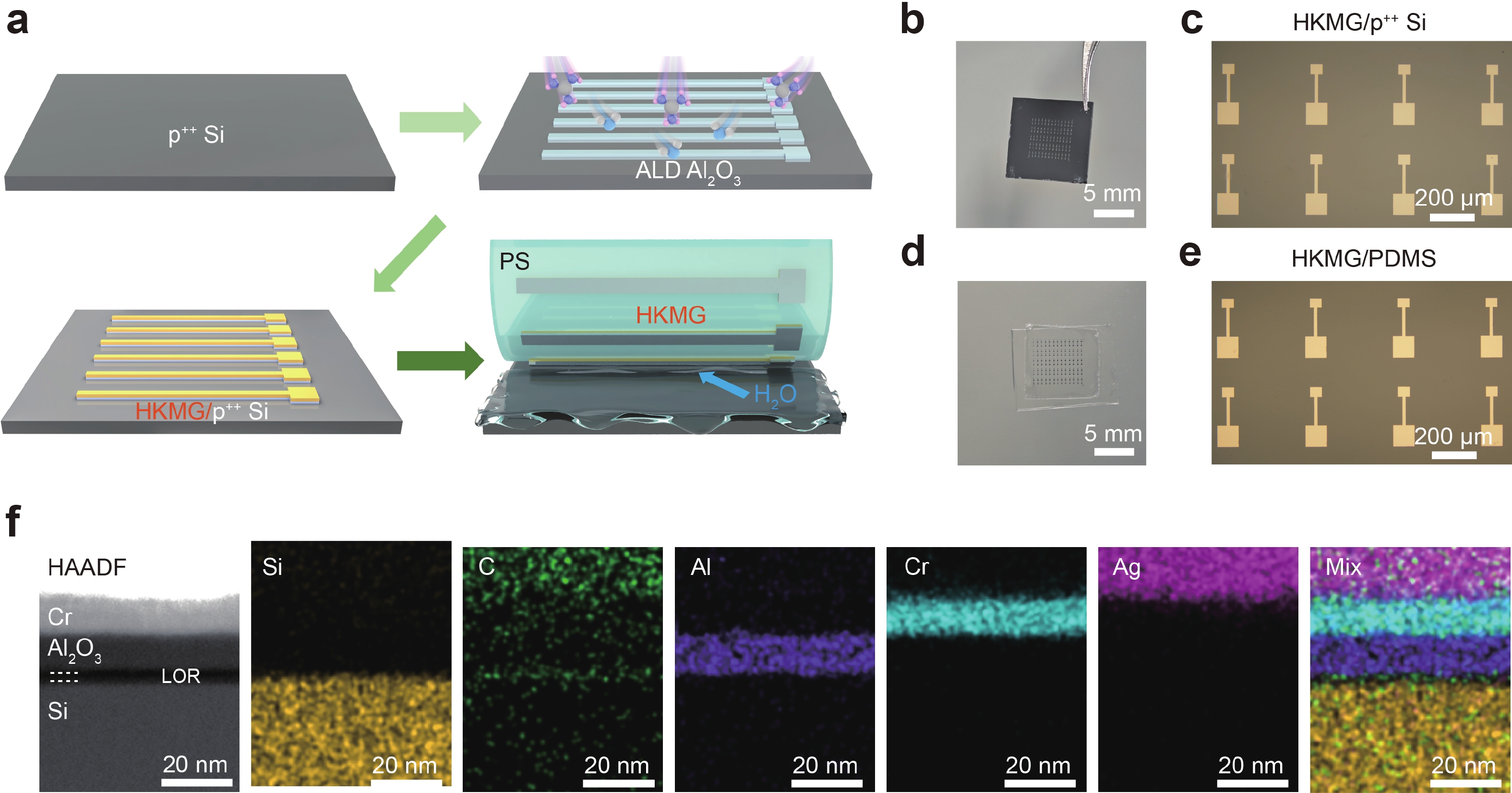
Fig. 3.  (Color online) Transfer of high-κ metal gate (HKMG) patterns on Si substrate. (a) Schematic illustration of the process flow for fabricating and transferring HKMG patterns on Si substrate. (b) and (c) Typical photograph (b) and corresponding OM image (c) of as-patterned HKMG (Al2O3/Cr/Ag) on Si substrate. (d) and (e) Typical photograph (d) and corresponding OM image (e) of the HKMG transferred onto the PS/PDMS supporter. (f) Cross-sectional high-angle annular dark-field (HAADF) image of the as-patterned HKMG on Si and corresponding EDS mapping images for the Si, C, Al, Cr, Ag, and mix elements, indicating the presence of LOR residual layer between the Si substrate and Al2O3.

Fig. 4.  (Color online) One-step transfer of entire device stack and van der Waals integration with MoS2. (a) Schematic of the one-step transfer and integrated process to fabricate fully encapsulated top-gated transistors. Typically, the source/drain contacts are In/Ag (5/30 nm) prepared by thermal evaporation, and the dielectric is 13 nm Al2O3 grown by atomic layer deposition (ALD). (b)−(f) Typical photograph and OM images of FET arrays fabricated on Si substrate (b), (e), capped with spin-coated PS films (c), (f) and peeled off to the PDMS supporter (d). (g) Typical AFM image of the backside of field-effect transistor (FET) arrays transferred onto PDMS, showing a surface roughness of 0.36 nm for the Al2O3. (h) Typical OM image of a top-gated MoS2 FET fabricated on SiO2/Si substrate by one-step transfer. (i) Cross-sectional HAADF and corresponding EDS mapping images for the Si, S, C, and Al elements. The clear C element signal at the interface between the MoS2 and Al2O3 suggests that the LOR residual layer was transferred off from Si substrate and stacked on top of MoS2 surface.

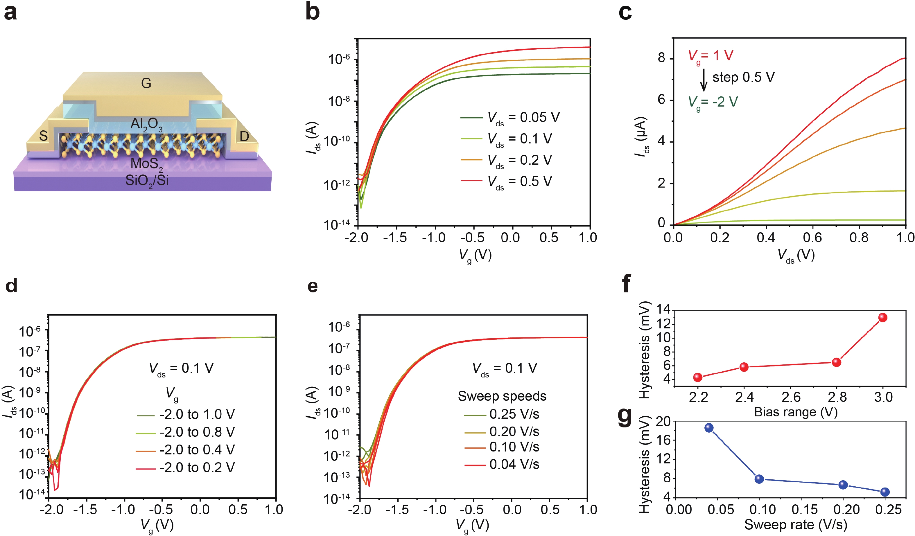
Fig. 5.  (Color online) MoS2 top-gate transistor fabricated via the one-step transfer and integration process. (a) Schematic illustration of the fabricated top-gate MoS2 transistor, whose contact and top-gate metals are In/Ag (5/30 nm) and Cr/Ag (8/45 nm), respectively. The MoS2 channel has a thickness of ~5 nm, and the thickness of Al2O3 was 13 nm. (b) Typical dual-sweep transfer curves of the MoS2 FET measured under different Vds from 0.05 to 0.5 V. (c) Corresponding output curves measured under different gate voltages (Vg) ranging from 1 to −2 V with a Vg step of −0.5 V. (d) and (e) Dual-sweep transfer curves of the MoS2 FET with different Vg sweeping ranges (d) and sweeping rates (e). (f) and (g) Extracted gate hysteresis as a function of the bias range (f) and the sweep rate (g).

[1]
Liu Y, Duan X D, Shin H J, et al. Promises and prospects of two-dimensional transistors. Nature, 2021, 591(7848): 43 doi: 10.1038/s41586-021-03339-z
[2]
Ma L K, Wang Y L, Liu Y. Van der Waals contact for two-dimensional transition metal dichalcogenides. Chem Rev, 2024, 124(5): 2583 doi: 10.1021/acs.chemrev.3c00697
[3]
Das S, Sebastian A, Pop E, et al. Transistors based on two-dimensional materials for future integrated circuits. Nat Electron, 2021, 4(11): 786 doi: 10.1038/s41928-021-00670-1
[4]
Liu C S, Chen H W, Wang S Y, et al. Two-dimensional materials for next-generation computing technologies. Nat Nanotechnol, 2020, 15(7): 545 doi: 10.1038/s41565-020-0724-3
[5]
Duan X D, Wang C, Pan A L, et al. Two-dimensional transition metal dichalcogenides as atomically thin semiconductors: Opportunities and challenges. Chem Soc Rev, 2015, 44(24): 8859 doi: 10.1039/C5CS00507H
[6]
Chen J B, Liu Z C, Dong X Y, et al. Vertically grown ultrathin Bi2SiO5 as high-κ single-crystalline gate dielectric. Nat Commun, 2023, 14(1): 4406 doi: 10.1038/s41467-023-40123-1
[7]
Wang Y, Sarkar S, Yan H, et al. Critical challenges in the development of electronics based on two-dimensional transition metal dichalcogenides. Nat Electron, 2024, 7(8): 638 doi: 10.1038/s41928-024-01210-3
[8]
Wang S Y, Liu X X, Xu M S, et al. Two-dimensional devices and integration towards the silicon lines. Nat Mater, 2022, 21(11): 1225 doi: 10.1038/s41563-022-01383-2
[9]
Poddar P K, Zhong Y, Mannix A J, et al. Resist-free lithography for monolayer transition metal dichalcogenides. Nano Lett, 2022, 22(2): 726 doi: 10.1021/acs.nanolett.1c04081
[10]
Nakatani M, Fukamachi S, Solís-Fernández P, et al. Ready-to-transfer two-dimensional materials using tunable adhesive force tapes. Nat Electron, 2024, 7(2): 119 doi: 10.1038/s41928-024-01121-3
[11]
Wang Y, Kim J C, Li Y, et al. P-type electrical contacts for 2D transition-metal dichalcogenides. Nature, 2022, 610(7930): 61 doi: 10.1038/s41586-022-05134-w
[12]
Shen P C, Su C, Lin Y X, et al. Ultralow contact resistance between semimetal and monolayer semiconductors. Nature, 2021, 593(7858): 211 doi: 10.1038/s41586-021-03472-9
[13]
Yang Z L, Huang B C, Lin Y K, et al. Directly probing the carrier transfer length in 2D-material transistors. Nature, 2026, 655(8122): 350 doi: 10.1038/s41586-026-10707-0
[14]
Zhang L, Liu Z C, Ai W, et al. Vertically grown metal nanosheets integrated with atomic-layer-deposited dielectrics for transistors with subnanometre capacitance-equivalent thicknesses. Nat Electron, 2024, 7(8): 662 doi: 10.1038/s41928-024-01202-3
[15]
Xu Y S, Liu T, Liu K L, et al. Scalable integration of hybrid high-κ dielectric materials on two-dimensional semiconductors. Nat Mater, 2023, 22(9): 1078 doi: 10.1038/s41563-023-01626-w
[16]
Li W S, Zhou J, Cai S H, et al. Uniform and ultrathin High-κ gate dielectrics for two-dimensional electronic devices. Nat Electron, 2019, 2(12): 563 doi: 10.1038/s41928-019-0334-y
[17]
Sim K, Chen S, Li Z W, et al. Three-dimensional curvy electronics created using conformal additive stamp printing. Nat Electron, 2019, 2(10): 471 doi: 10.1038/s41928-019-0304-4
[18]
Meitl M A, Zhu Z T, Kumar V, et al. Transfer printing by kinetic control of adhesion to an elastomeric stamp. Nat Mater, 2005, 5(1): 33
[19]
Shin Y, Hong S, Hur Y C, et al. Damage-free dry transfer method using stress engineering for high-performance flexible two- and three-dimensional electronics. Nat Mater, 2024, 23(10): 141
[20]
Liu G Y, Tian Z A, Yang Z Y, et al. Graphene-assisted metal transfer printing for wafer-scale integration of metal electrodes and two-dimensional materials. Nat Electron, 2022, 5(5): 275 doi: 10.1038/s41928-022-00764-4
[21]
Liu Y, Guo J, Zhu E B, et al. Approaching the Schottky–Mott limit in van der Waals metal–semiconductor junctions. Nature, 2018, 557(7707): 696 doi: 10.1038/s41586-018-0129-8
[22]
Yang X D, Li J, Song R, et al. Highly reproducible van der Waals integration of two-dimensional electronics on the wafer scale. Nat Nanotechnol, 2023, 18(5): 471 doi: 10.1038/s41565-023-01342-1
[23]
Zeng D B, Zhang Z Y, Xue Z Y, et al. Single-crystalline metal-oxide dielectrics for top-gate 2D transistors. Nature, 2024, 632(8026): 788 doi: 10.1038/s41586-024-07786-2
[24]
Qi D Y, Li P, Ou H H, et al. Graphene-enhanced metal transfer printing for strong van der Waals contacts between 3D metals and 2D semiconductors. Adv Funct Mater, 2023, 33(27): 2301704 doi: 10.1002/adfm.202301704
[25]
Wu Y H, Xin Z Q, Zhang Z B, et al. All-transfer electrode interface engineering toward harsh-environment-resistant MoS2 field-effect transistors. Adv Mater, 2023, 35(18): 2210735 doi: 10.1002/adma.202210735
[26]
Wang L Y, Wang P Q, Huang J, et al. A general one-step plug-and-probe approach to top-gated transistors for rapidly probing delicate electronic materials. Nat Nanotechnol, 2022, 17(11): 1206 doi: 10.1038/s41565-022-01221-1
[27]
Kwon G, Choi Y H, Lee H, et al. Interaction- and defect-free van der waals contacts between metals and two-dimensional semiconductors. Nat Electron, 2022, 5(4): 241 doi: 10.1038/s41928-022-00746-6
[28]
Hong M Y, Zhang X K, Geng Y, et al. Universal transfer of full-class metal electrodes for barrier-free two-dimensional semiconductor contacts. InfoMat, 2023, 6(1): e12491
[29]
Kong L G, Wu R X, Chen Y, et al. Wafer-scale and universal van der Waals metal semiconductor contact. Nat Commun, 2023, 14(1): 1014 doi: 10.1038/s41467-023-36715-6
[30]
Lu Z Y, Chen Y, Dang W Q, et al. Wafer-scale high-κ dielectrics for two-dimensional circuits via van der Waals integration. Nat Commun, 2023, 14(1): 2340 doi: 10.1038/s41467-023-37887-x
[31]
Xing K J, McEwen D, Yin Y F, et al. Pick-and-place transfer of arbitrary-metal electrodes for van der Waals device fabrication. ACS Nano, 2025, 19(3): 3579 doi: 10.1021/acsnano.4c13592
[32]
Zhang X D, Huang C X, Li Z Y, et al. Reliable wafer-scale integration of two-dimensional materials and metal electrodes with van der Waals contacts. Nat Commun, 2024, 15(1): 4619 doi: 10.1038/s41467-024-49058-7
[33]
Yan Y J, Yan T, Wang F, et al. Cmos-compatible fabrication of 2D semiconductor-based cfets via High-κ dielectric van der Waals encapsulation. Nano Lett, 2025, 25(15): 6125 doi: 10.1021/acs.nanolett.5c00220
[34]
He Y Y, Lv Z X, Liu Z C, et al. Sacrifice-layer-free transfer of wafer-scale atomic-layer-deposited dielectrics and full-device stacks for two-dimensional electronics. Nat Commun, 2025, 16(1): 5904 doi: 10.1038/s41467-025-60864-5
[35]
Jiang J F, Wu P, Liu Y F, et al. Towards fab-compatible two-dimensional electronics. Nat Rev Electr Eng, 2025, 2(1): 6 doi: 10.1038/s44287-024-00125-7
[36]
Hwang E, Hong H, Lee Y, et al. Van der Waals materials for energy-efficient electronic devices. Nature Reviews Materials, 2026, 11(4): 308 doi: 10.1038/s41578-025-00886-z
[37]
Kim K S, Kwon J, Ryu H, et al. The future of two-dimensional semiconductors beyond Moore’s law. Nat Nanotechnol, 2024, 19(7): 895 doi: 10.1038/s41565-024-01695-1
[38]
Li Y F, Liu S Q, Zheng H, et al. From planar to 3D: The evolution of complementary field-effect transistor for next-generation semiconductor nodes. Adv Mater, 2026, 38(32): e73226 doi: 10.1002/adma.73226
[39]
Zeng S F, Liu C S, Huang X H, et al. An application-specific image processing array based on WSe2 transistors with electrically switchable logic functions. Nat Commun, 2022, 13(1): 56 doi: 10.1038/s41467-021-27644-3
[40]
Xu M S, Wang Y W, Liu J W, et al. Progress on the program of Si-compatible two-dimensional semiconductor materials and devices. Sci China Inf Sci, 2024, 67(6): 160401 doi: 10.1007/s11432-024-3986-8
[41]
Xia X X, Yang H F, Sun Y M, et al. Fabrication of terahertz metamaterials using S1813/LOR stack by lift-off. Microelectron Eng, 2008, 85(5): 1433
[42]
Chen Y F, Peng K W, Cui, Z. A lift-off process for high resolution patterns using pmma/LOR resist stack. Microelectron Eng, 2004, 73: 278
[43]
Preiss E M, Krauss A, Seidel H. Sputtered Pt electrode structures with smoothly tapered edges by bi-layer resist lift-off. Thin Solid Films, 2015, 597: 158 doi: 10.1016/j.tsf.2015.11.026
[44]
Lyytinen J, Berdova M, Hirvonen P, et al. Interfacial mechanical testing of atomic layer deposited TiO2 and Al2O3 on a silicon substrate by the use of embedded SiO2 microspheres. RSC Adv, 2014, 4(70): 37320 doi: 10.1039/C4RA05807K
[45]
Venkatakrishnarao D, Mishra A, Tarn Y, et al. Liquid metal oxide-assisted integration of high-κ dielectrics and metal contacts for two-dimensional electronics. ACS Nano, 2024, 18(39): 26911 doi: 10.1021/acsnano.4c08554
[46]
Kawanago T, Oba T, Oda S. Transfer printing of Al2O3 gate dielectric for fabrication of top-gate MoS2 FET. Appl Phys Express, 2019, 12(2): 026501 doi: 10.7567/1882-0786/aaf995
[47]
Jung H, Park J, Oh I K, et al. Fabrication of transferable Al2O3 nanosheet by atomic layer deposition for graphene FET. ACS Appl Mater Interfaces, 2014, 6(4): 2764 doi: 10.1021/am4052987
[48]
Schauble K, Zakhidov D, Yalon E, et al. Uncovering the effects of metal contacts on monolayer MoS2. ACS Nano, 2020, 14(11): 14798 doi: 10.1021/acsnano.0c03515
[49]
Bartlett P N, Kees de Groot C H K, Greenacre V K, et al. Molecular precursors for the electrodeposition of 2D-layered metal chalcogenides. Nat Rev Chem, 2025, 9(2): 88 doi: 10.1038/s41570-024-00671-6
[50]
Yang S J, Liu K L, Xu Y S, et al. Gate dielectrics integration for 2D electronics: Challenges, advances, and outlook. Adv Mater, 2023, 35(18): 2207901 doi: 10.1002/adma.202207901
[51]
Wang Y, Kim J C, Wu R J, et al. Van der Waals contacts between three-dimensional metals and two-dimensional semiconductors. Nature, 2019, 568(7750): 70 doi: 10.1038/s41586-019-1052-3
[52]
Liu M R, Wang Y N , Hong M Y, et al. Noninvasive van der Waals interface integrations for intrinsic 2D semiconductor characterization. Nano Lett, 2025, 25(40): 14677 doi: 10.1021/acs.nanolett.5c03799
[53]
Wang B X, Yu H, Wang C, et al. Top-gated monolayer MoS2 transistors on growth substrate by one-step integration of high-κ dielectrics and low-resistance bilayer contacts. Nano Lett, 2026, 26(18): 6081 doi: 10.1021/acs.nanolett.6c00542
  • Search

    Advanced Search >>

    GET CITATION

    shu

    Export: BibTex EndNote

    Article Metrics

    Article views: 4 Times PDF downloads: 1 Times Cited by: 0 Times

    History

    Received: 27 August 2026 Revised: 22 September 2026 Online: Accepted Manuscript: 12 October 2026

    Catalog

      Email This Article

      User name:
      Email:*请输入正确邮箱
      Code:*验证码错误
      Zunxian Lv, Shun Zhang, Mingjian Yang, Xinsheng Wang, Zhaochao Liu, Yameng Hou, Jiabiao Chen, Moyuan Cao, Feng Luo, Jinxiong Wu. A photolithography-compatible method for transferring full-device constituents on silicon substrate[J]. Journal of Semiconductors, 2026, In Press. doi: 10.1088/1674-4926/26080030 ****Z Lv, S Zhang, M J Yang, X S Wang, Z C Liu, Y M Hou, J B Chen, M Y Cao, F Luo, and J X Wu, A photolithography-compatible method for transferring full-device constituents on silicon substrate[J]. J. Semicond., 2026, 47(10): 102709 doi: 10.1088/1674-4926/26080030
      Citation:
      Zunxian Lv, Shun Zhang, Mingjian Yang, Xinsheng Wang, Zhaochao Liu, Yameng Hou, Jiabiao Chen, Moyuan Cao, Feng Luo, Jinxiong Wu. A photolithography-compatible method for transferring full-device constituents on silicon substrate[J]. Journal of Semiconductors, 2026, In Press. doi: 10.1088/1674-4926/26080030 ****
      Z Lv, S Zhang, M J Yang, X S Wang, Z C Liu, Y M Hou, J B Chen, M Y Cao, F Luo, and J X Wu, A photolithography-compatible method for transferring full-device constituents on silicon substrate[J]. J. Semicond., 2026, 47(10): 102709 doi: 10.1088/1674-4926/26080030

      A photolithography-compatible method for transferring full-device constituents on silicon substrate

      DOI: 10.1088/1674-4926/26080030
      CSTR: 32376.14.1674-4926.26080030
      More Information
      • Zunxian Lv is a PhD candidate at the School of Materials Science and Engineering, Nankai University. He is currently conducting her research under the supervision of Prof. Jinxiong Wu at Nankai University. His research focuses on transfer and integration of 2D Materials
      • Jiabiao Chen got his B.S. degree in 2021 and Ph.D. degree in 2026 at Nankai University. Now he is a postdoctoral researcher at Nankai University under the supervision of Prof. Jinxiong Wu. His research interests include the development of 2D gate-dielectric materials and high-performance nanoelectronics
      • Jinxiong Wu has been a Professor at the School of Materials Science and Engineering, Nankai University, since 2019. He obtained his Ph.D. degree in Physical Chemistry from Peking University at 2017, then continued his postdoctoral program in the same University during 2017~2019. His research focuses on high-mobility and high-κ 2D materials based functional devices
      • Corresponding author: jbchen@nankai.edu.cn; jxwu@nankai.edu.cn
      • Received Date: 2026-08-27
      • Revised Date: 2026-09-22
      • Available Online: 2026-10-12

      Catalog

        /

        DownLoad:  Full-Size Img  PowerPoint
        Return
        Return