Issue Browser
Volume 47, Issue 10, Oct 2026
EDITORIAL
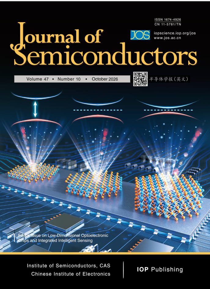
Preface to the Focus Issue on Low-Dimensional Optoelectronic Chips and Integrated Intelligent Sensing
Qianlong Kang, Zhen Wang, Guangjian Wu, Congwei Tan, Tiange Zhao, Hangyu Xu
J. Semicond.  2026, 47(10): 100101  doi: 10.1088/1674-4926/26101001

REVIEWS
Functional photoelectronic devices: leveraging two-dimensional van der Waals device configuration
Yuanfang Yu, Jiaxin Gong, Senyao Tang, Yuan Gao, Nanjie Jiang, Haiyan Nan
J. Semicond.  2026, 47(10): 101701  doi: 10.1088/1674-4926/26060030

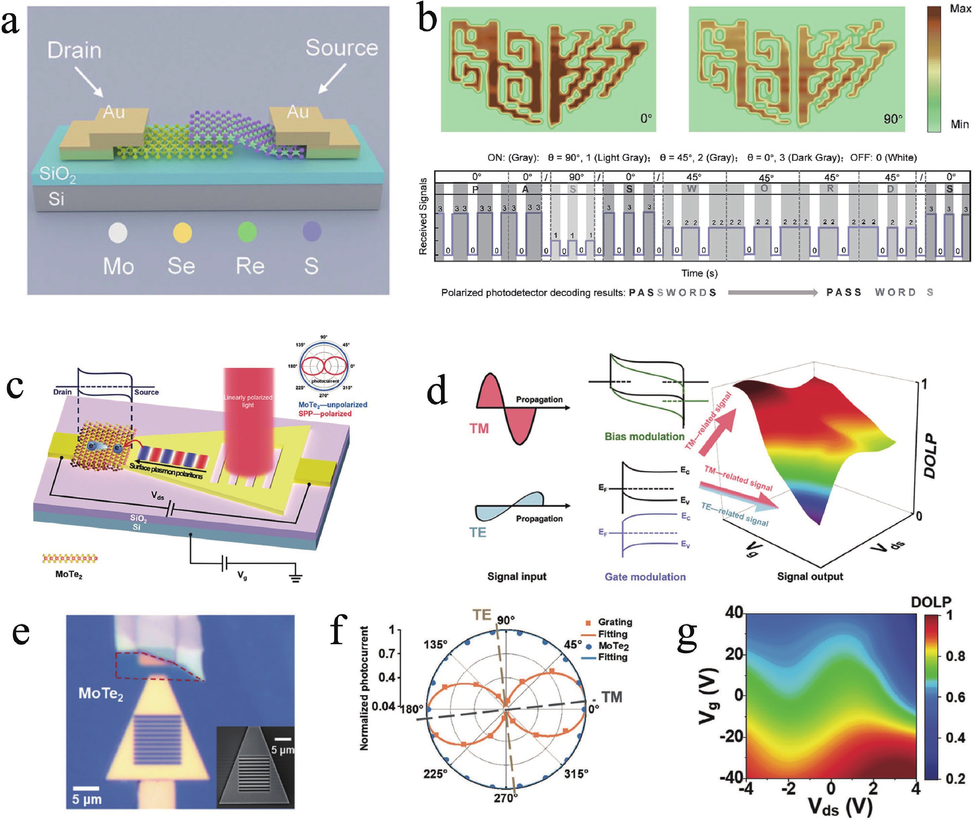
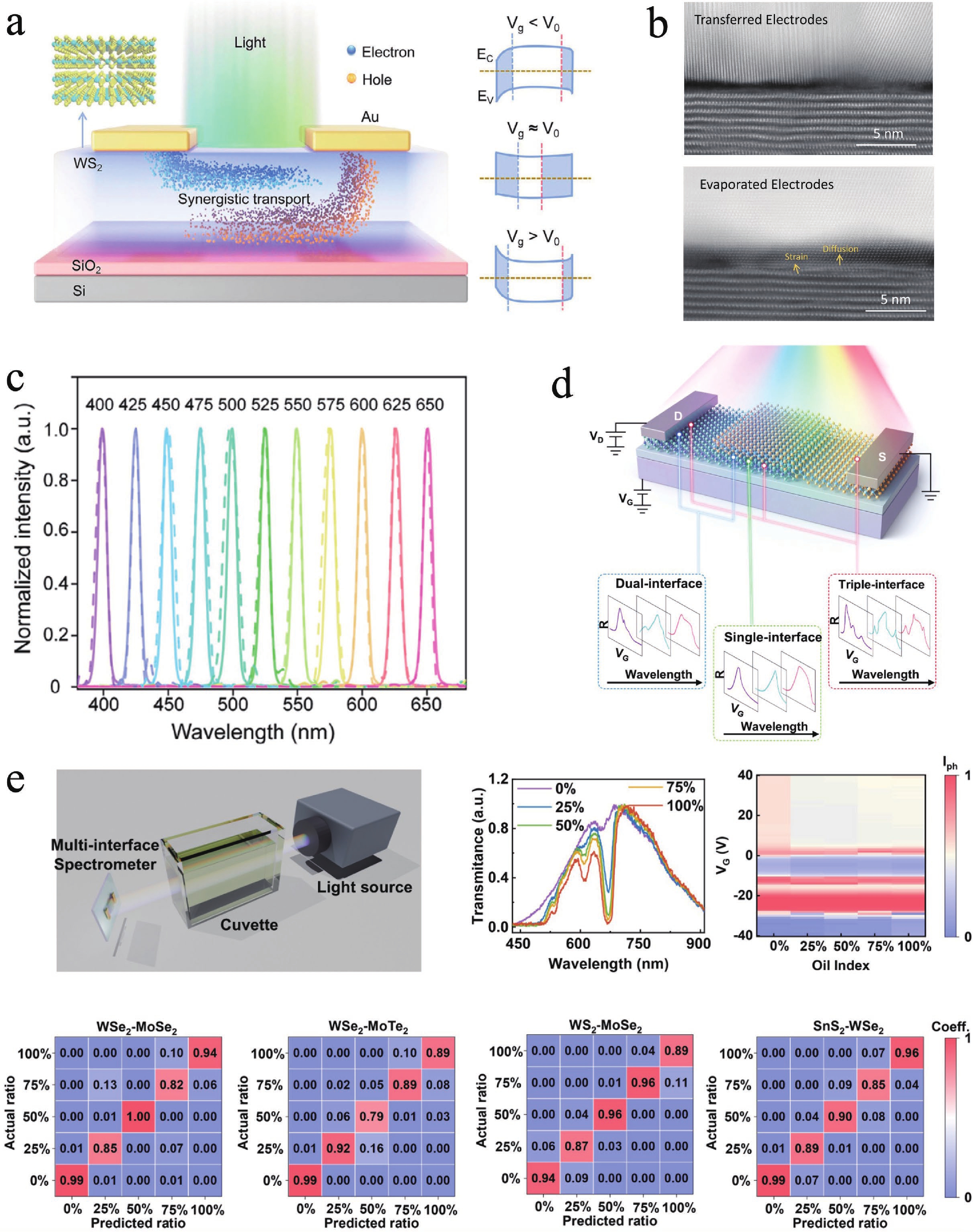
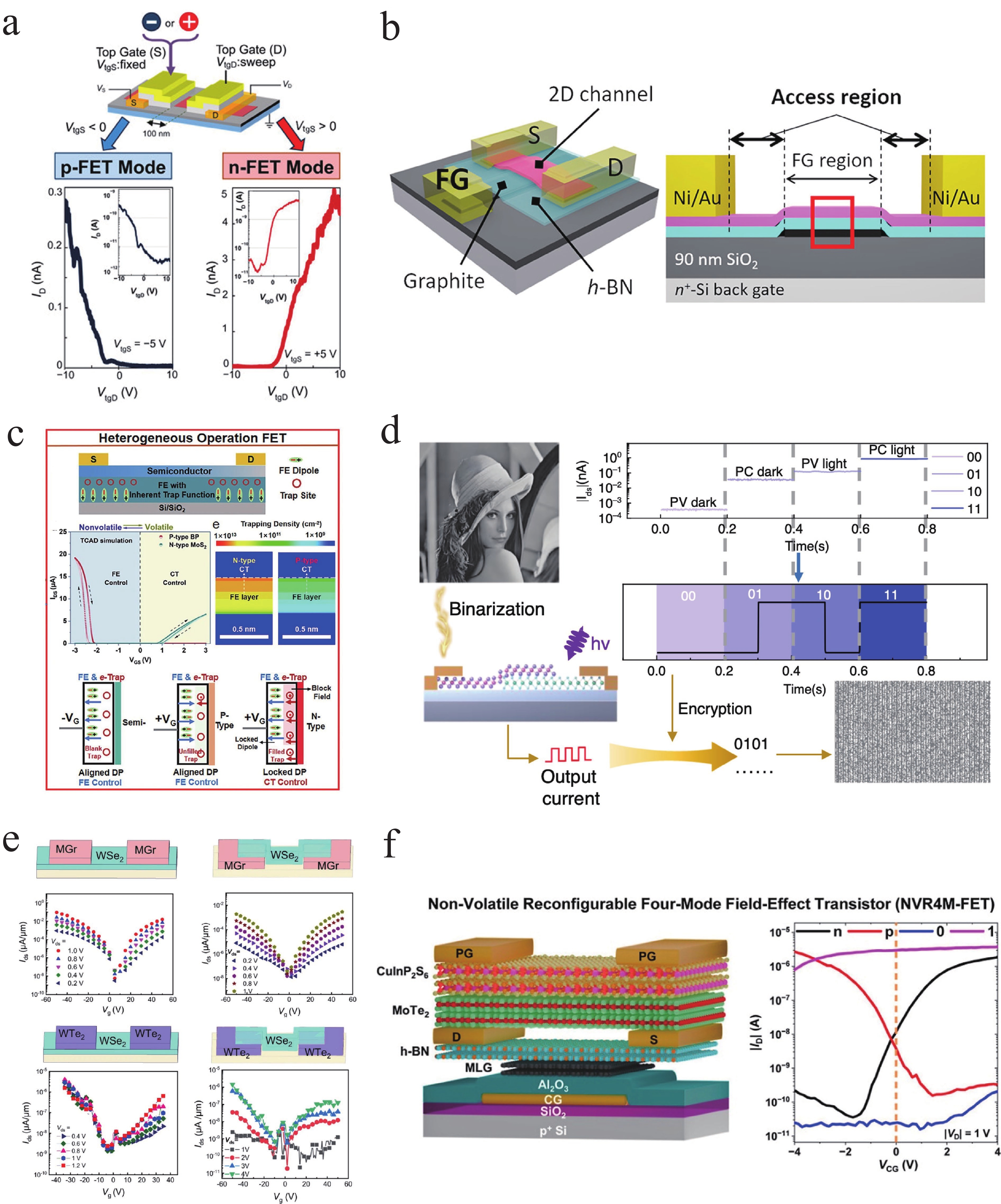
Two-dimensional (2D) van der Waals (vdW) materials offer atomically thin, dangling-bond-free interfaces and strong electrostatic control characteristics, enabling a new paradigm for optoelectronic devices. This review focuses on vdW contact engineering and heterostructure construction. The vdW contact can suppress Fermi-level pinning, reduce contact resistance, and preserve the intrinsic properties of 2D semiconductors. Leveraging such clean interfaces, 2D vdW materials show great potential in implementing functional devices, including photodetectors, miniaturized computational spectrometers, reconfigurable devices, and neuromorphic systems. In these cases, the tunable vdW interfaces eliminate lattice-matching constraints and allow feasible heterogeneous integration. This review discusses the recent progress and future prospects in this field, providing guidance for realizing functional applications based on vdW device configuration.
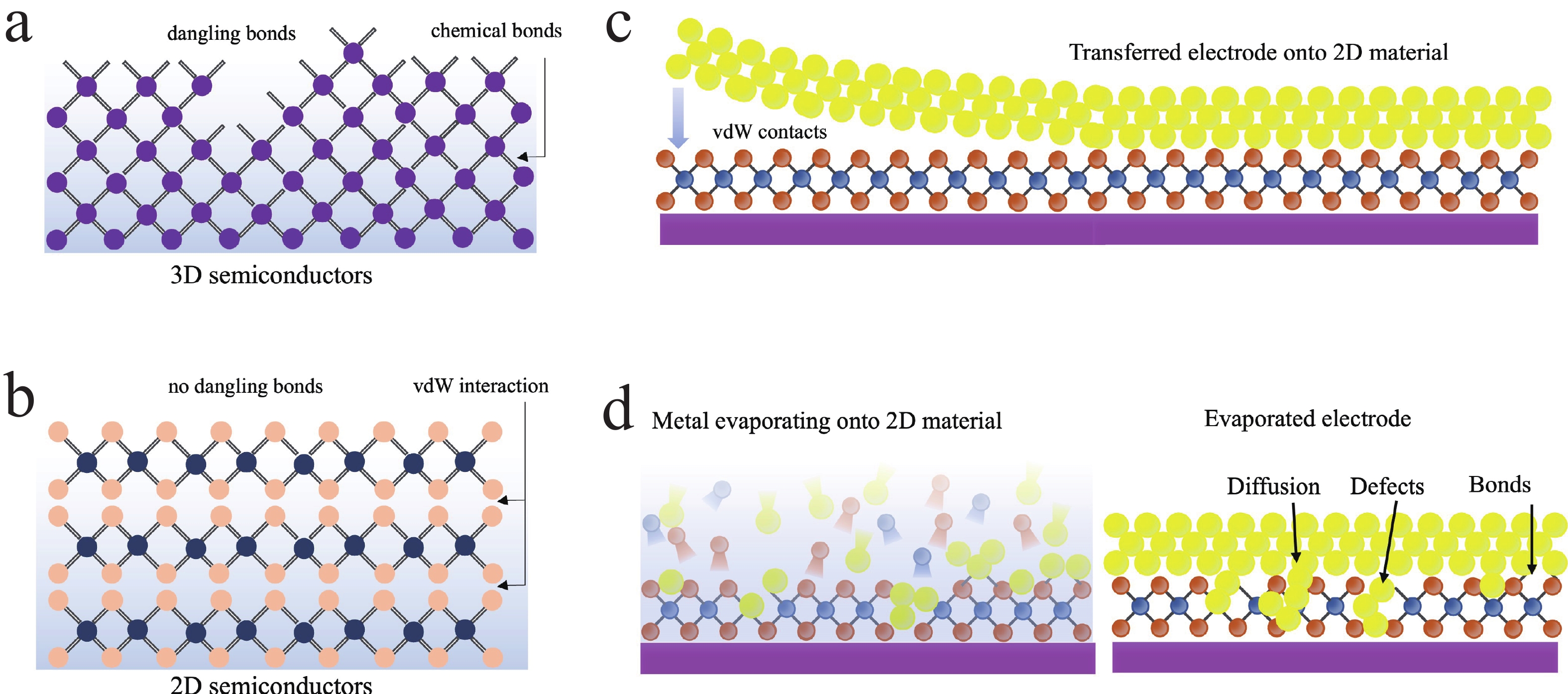
Two-dimensional (2D) van der Waals (vdW) materials offer atomically thin, dangling-bond-free interfaces and strong electrostatic control characteristics, enabling a new paradigm for optoelectronic devices. This review focuses on vdW contact engineering and heterostructure construction. The vdW contact can suppress Fermi-level pinning, reduce contact resistance, and preserve the intrinsic properties of 2D semiconductors. Leveraging such clean interfaces, 2D vdW materials show great potential in implementing functional devices, including photodetectors, miniaturized computational spectrometers, reconfigurable devices, and neuromorphic systems. In these cases, the tunable vdW interfaces eliminate lattice-matching constraints and allow feasible heterogeneous integration. This review discusses the recent progress and future prospects in this field, providing guidance for realizing functional applications based on vdW device configuration.
Low-dimensional perovskite optoelectronic synapses for neuromorphic vision
Zhihao Xu, Yingjie Luo, Alson Yau, Yuan Meng, Seung-il Kim, Kyubeen Kim, Sheng Ran, Sang-Hoon Bae
J. Semicond.  2026, 47(10): 101702  doi: 10.1088/1674-4926/26060035

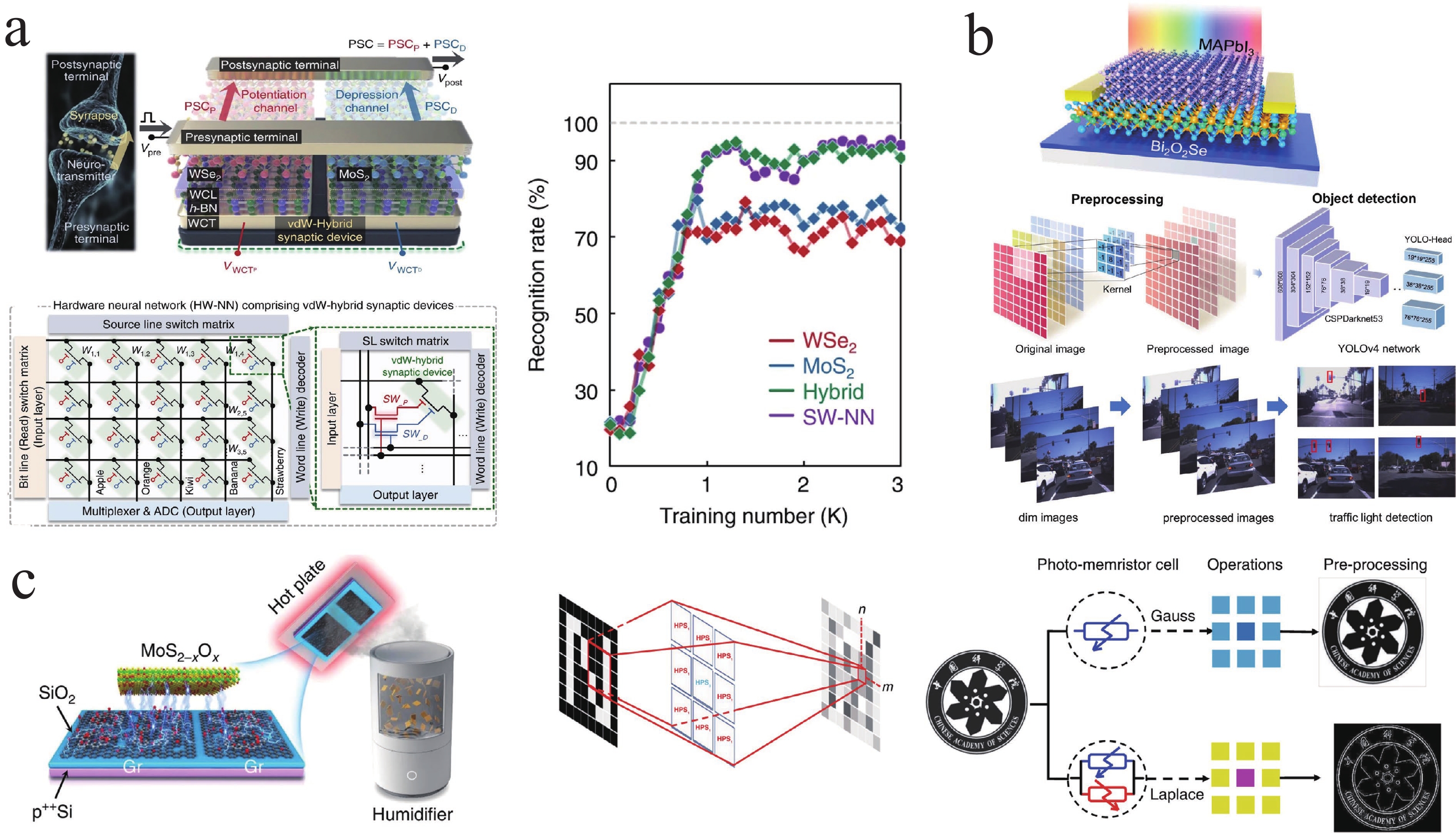
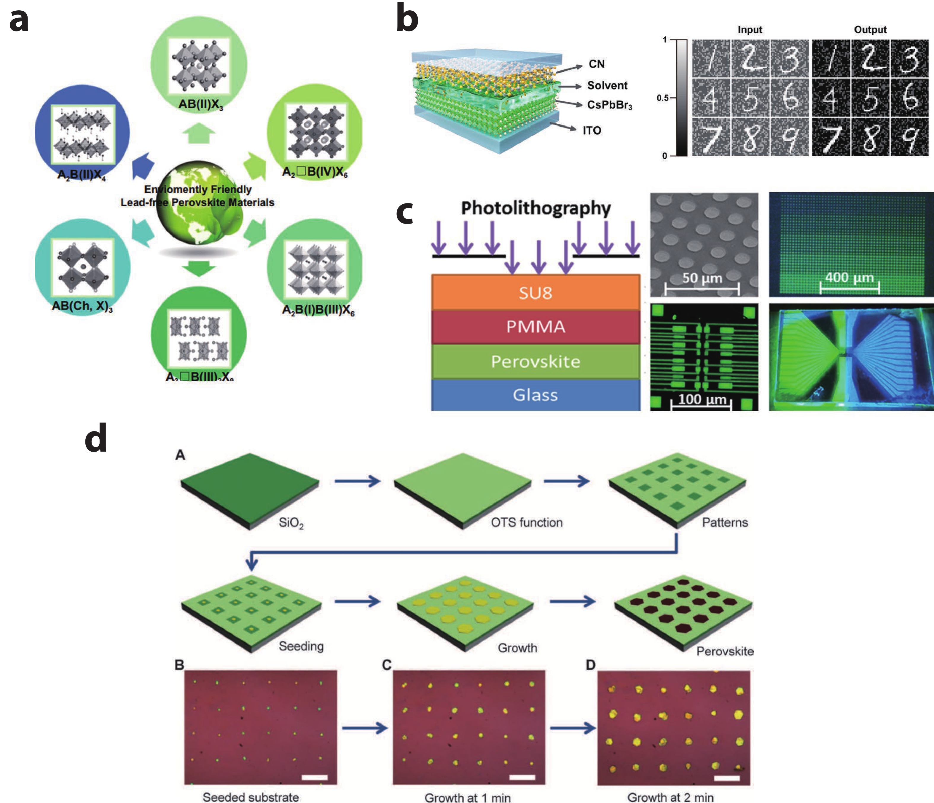
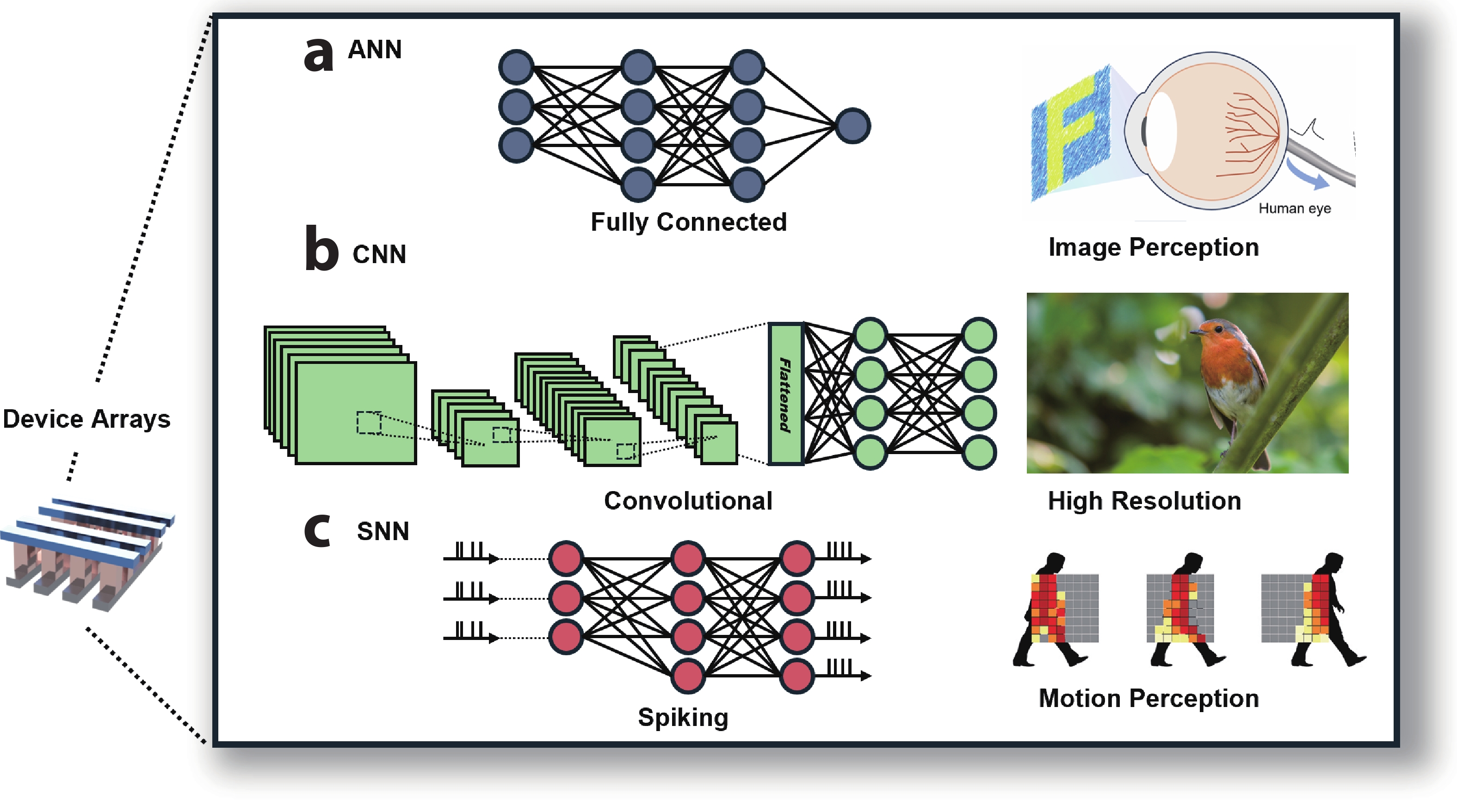
Low-dimensional metal-halide perovskites have emerged as promising materials for optoelectronic synapses and neuromorphic vision systems owing to their strong light–matter interactions, tunable optoelectronic properties, and mixed ionic–electronic transport. Compared with three-dimensional counterparts, low-dimensional perovskites exhibit more powerful control over charge transport, ion migration, and optical absorption with enhanced stability. In this review, we outline the composition, dimensionality, and growth strategies of low-dimensional perovskites, emphasizing how structural engineering governs their optical and electrical properties. Their photodetection, memristive, and photo-reservoir behaviors are further discussed to form physical foundation for light-stimulated synaptic functions, including optical sensing, memory retention, and conductance modulation. We review representative optoelectronic synapses based on 0D, 1D, and 2D perovskites according to their device-level mechanisms, highlighting how dimensionality enables distinct visual functions and device architectures. Exemplary neuromorphic algorithms are discussed as well, including artificial neural networks, convolutional neural networks, spiking neural networks, recurrent neural networks, and reservoir computing, which translate perovskite synaptic responses into higher-level capabilities such as image recognition, multimodal perception, and motion detection. Finally, we catalog the remaining challenges including lead toxicity, limited lead-free performance, crystallization and device-to-device variations, ion-migration-induced instability, and options for wafer-scale patterning and addressable integration. By connecting materials design, synaptic device physics, neuromorphic algorithms, and scalable integration strategies, with perspectives on how low-dimensional perovskites can evolve from laboratory-scale optoelectronic synapses into practical platforms for next-generation artificial vision systems.
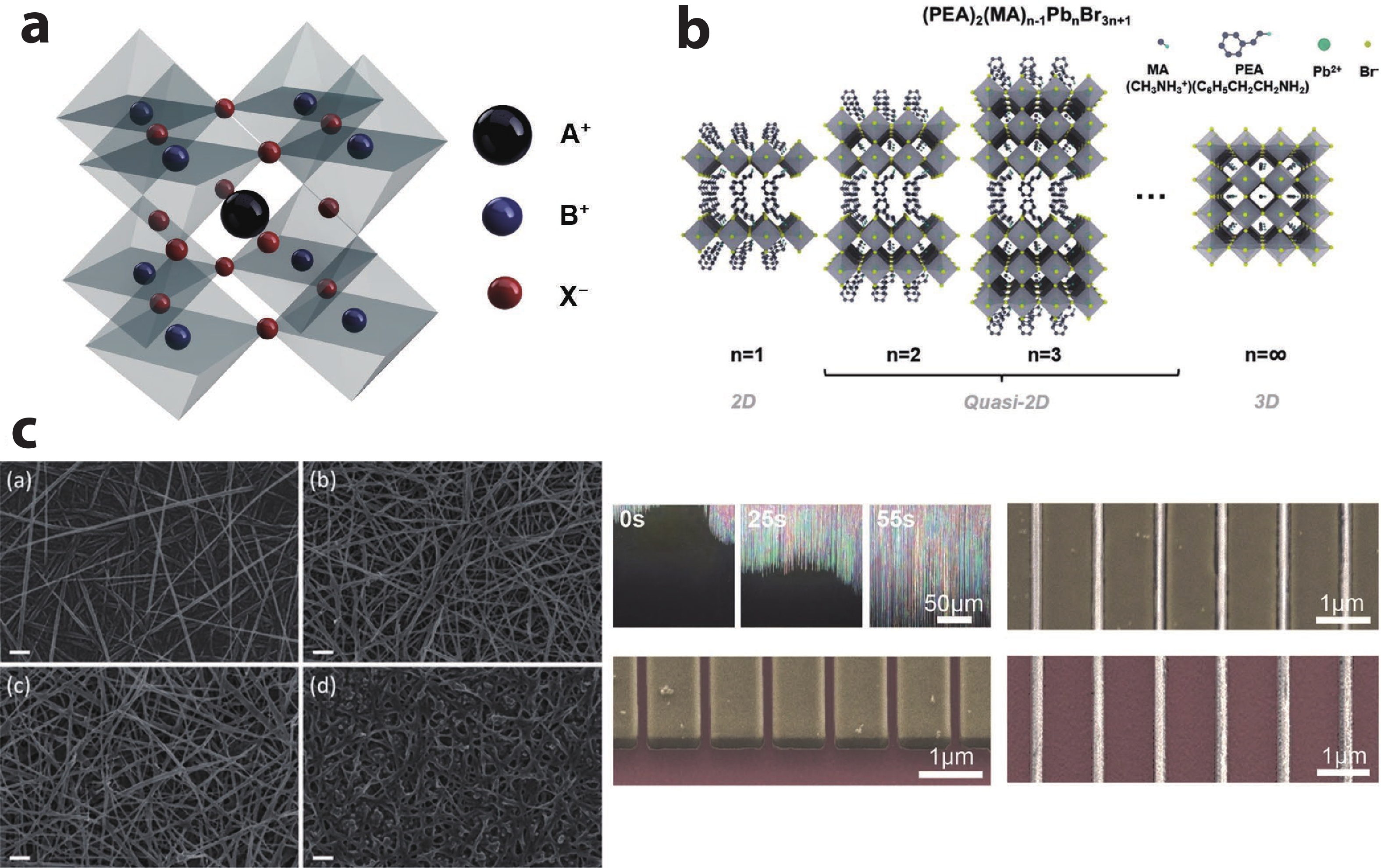
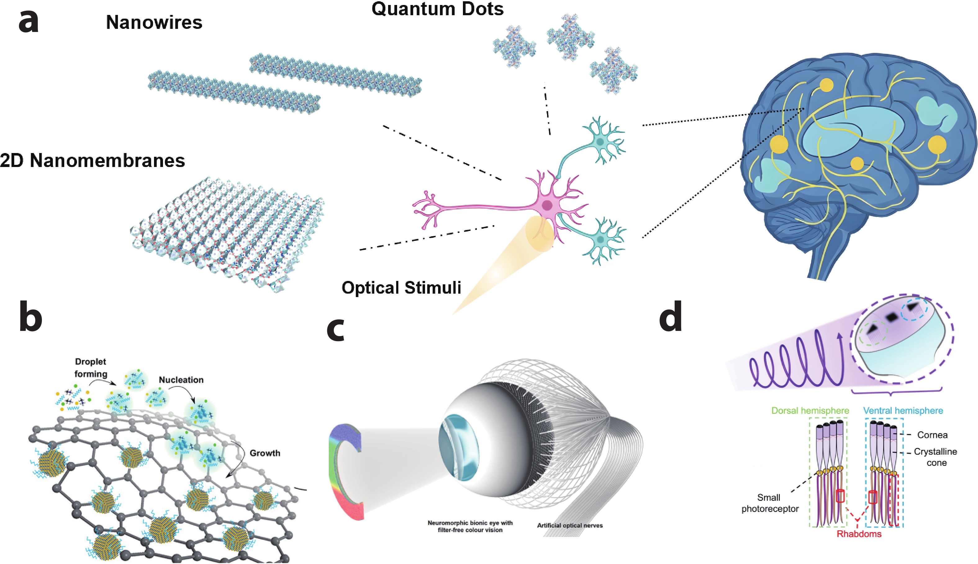
Low-dimensional metal-halide perovskites have emerged as promising materials for optoelectronic synapses and neuromorphic vision systems owing to their strong light–matter interactions, tunable optoelectronic properties, and mixed ionic–electronic transport. Compared with three-dimensional counterparts, low-dimensional perovskites exhibit more powerful control over charge transport, ion migration, and optical absorption with enhanced stability. In this review, we outline the composition, dimensionality, and growth strategies of low-dimensional perovskites, emphasizing how structural engineering governs their optical and electrical properties. Their photodetection, memristive, and photo-reservoir behaviors are further discussed to form physical foundation for light-stimulated synaptic functions, including optical sensing, memory retention, and conductance modulation. We review representative optoelectronic synapses based on 0D, 1D, and 2D perovskites according to their device-level mechanisms, highlighting how dimensionality enables distinct visual functions and device architectures. Exemplary neuromorphic algorithms are discussed as well, including artificial neural networks, convolutional neural networks, spiking neural networks, recurrent neural networks, and reservoir computing, which translate perovskite synaptic responses into higher-level capabilities such as image recognition, multimodal perception, and motion detection. Finally, we catalog the remaining challenges including lead toxicity, limited lead-free performance, crystallization and device-to-device variations, ion-migration-induced instability, and options for wafer-scale patterning and addressable integration. By connecting materials design, synaptic device physics, neuromorphic algorithms, and scalable integration strategies, with perspectives on how low-dimensional perovskites can evolve from laboratory-scale optoelectronic synapses into practical platforms for next-generation artificial vision systems.
ARTICLES
Ferroelectric α-Bi2O3 films derived from β-Bi via ultraviolet ozone oxidation
Wei Li, Wei Zhang, Lingyuan Kong, Tianci Hu, Zeguo Lin, Yi Jiang, Fang Yang, Yang Guo, Pan Chen, Runzhang Xu, Yan Liang, Jiandi Zhang
J. Semicond.  2026, 47(10): 102701  doi: 10.1088/1674-4926/26070002
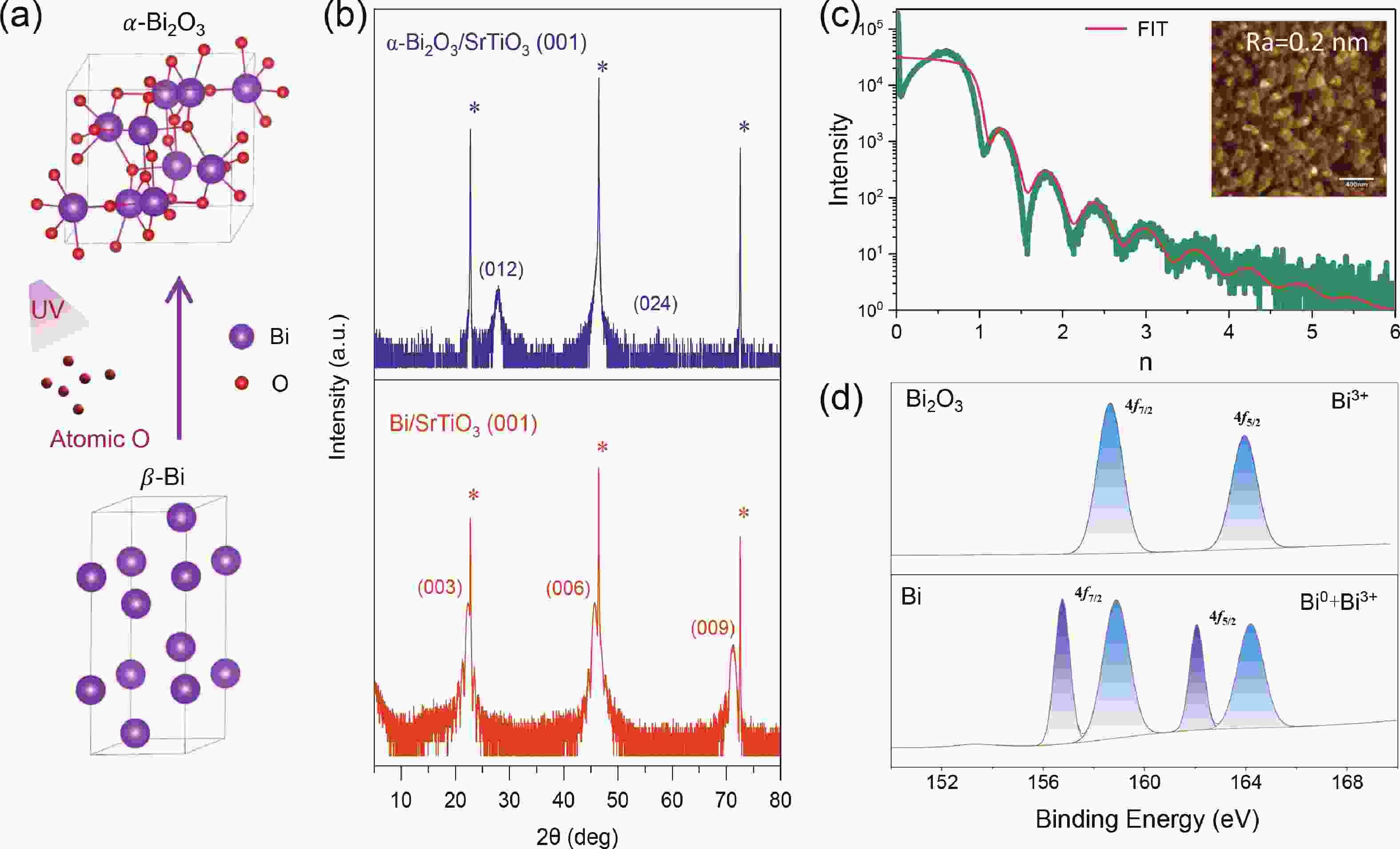
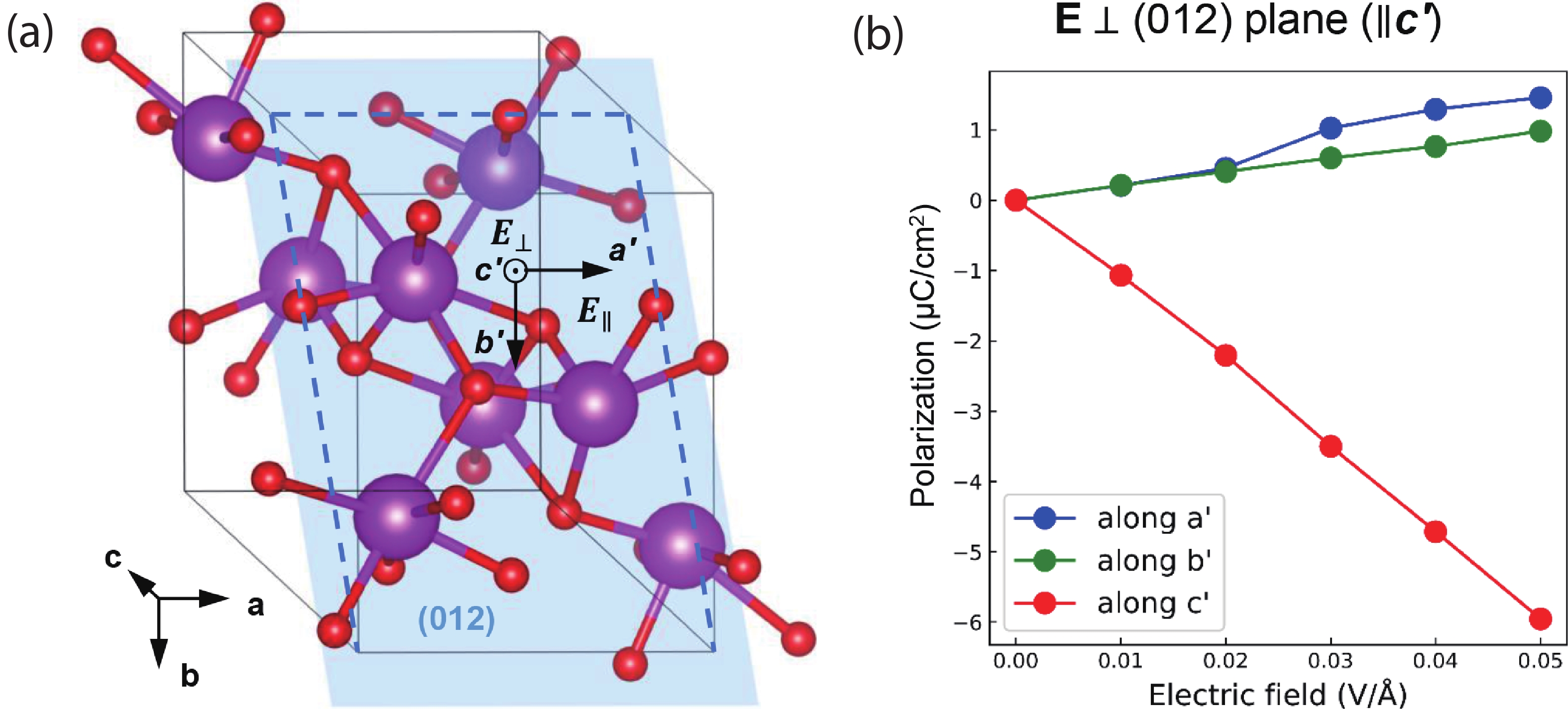
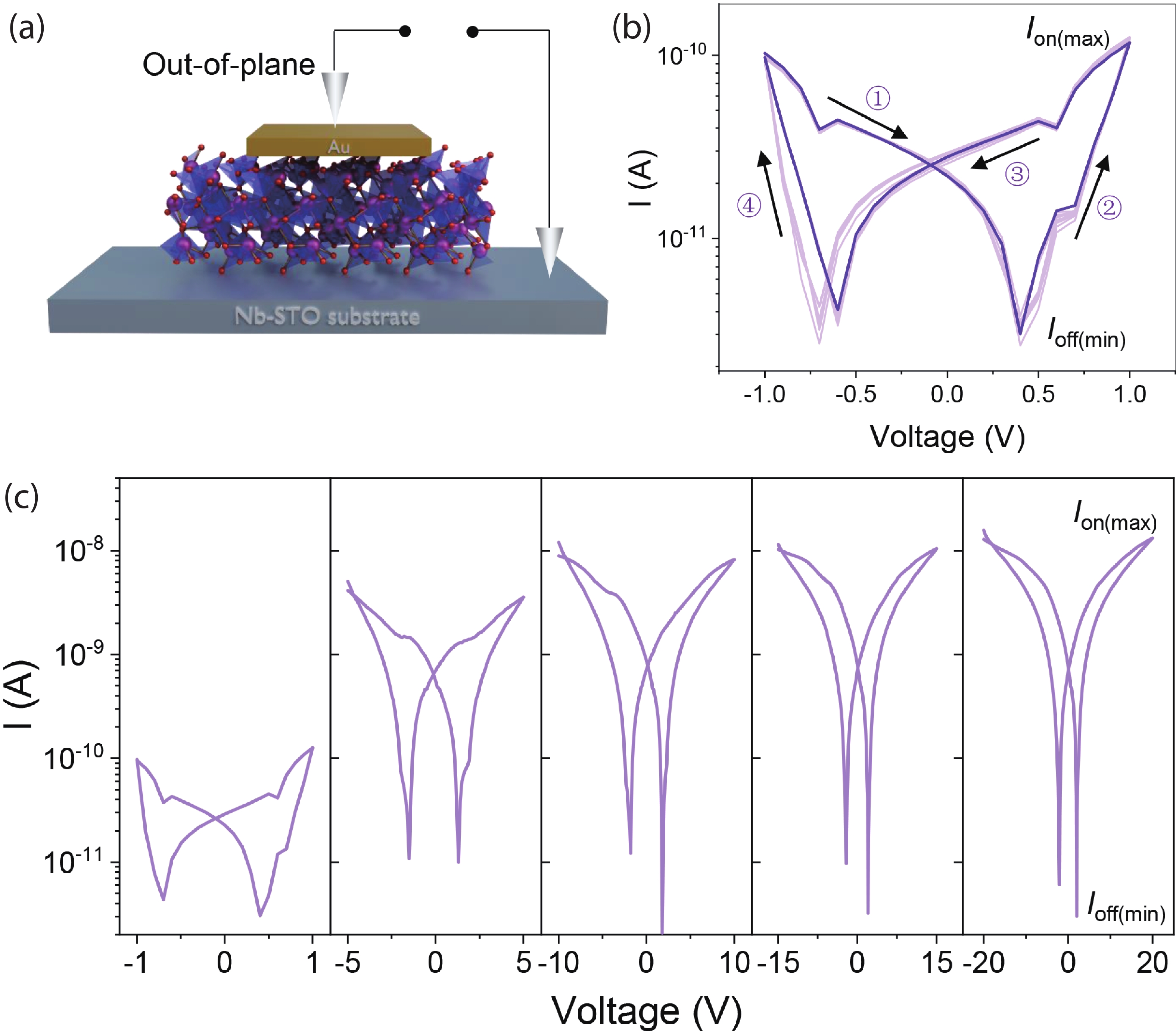
Bismuth-based oxides are well known for their high Curie temperature and excellent fatigue resistance, which have attracted extensive researches and various applications. In this work, we successfully fabricated pure phase α-Bi2O3 films by a novel ultraviolet ozone oxidation method from β-Bi. The obtained α-Bi2O3 exhibits room-temperature out-of-plane ferroelectricity, as confirmed by both piezoelectric force microscopy measurements and hysteresis loops obtained from out-of-plane ferroelectric tunnel junctions. Density functional calculations predict that the ferroelectricity of α-Bi2O3 arises from a synergistic interplay between electric-field-induced structural deformation and charge redistribution within films. Our results demonstrate that such a thin room-temperature ferroelectric α-Bi2O3 film could be a promising candidate for future multifunctional electronic devices.
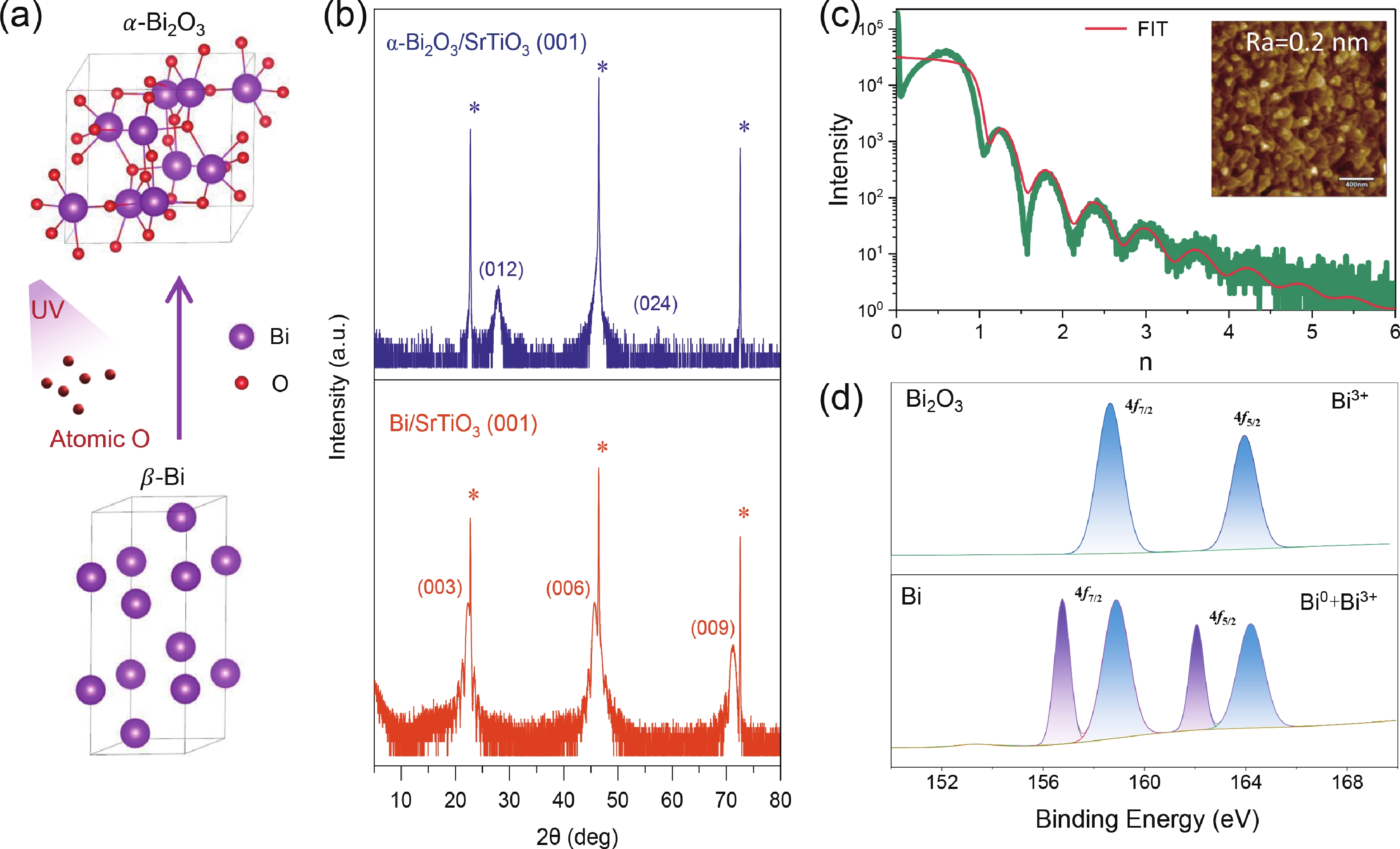
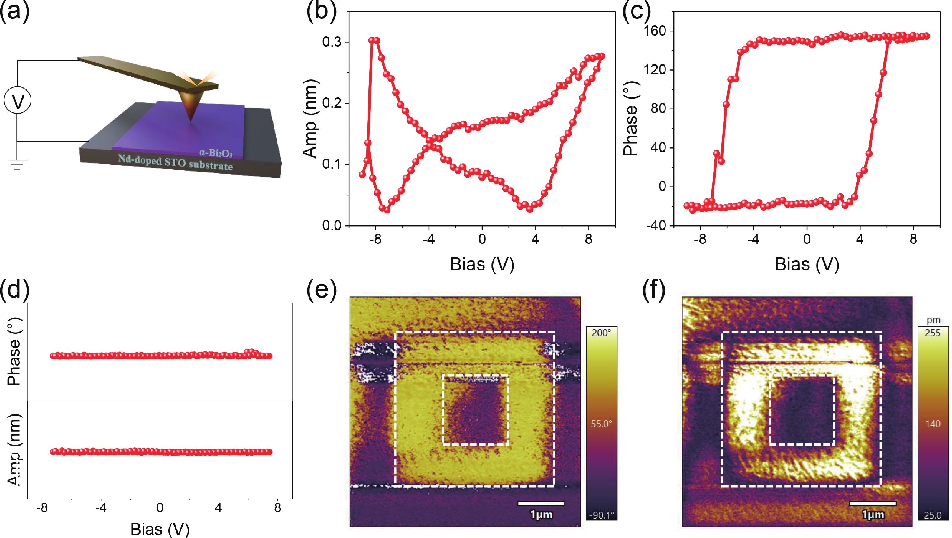
Bismuth-based oxides are well known for their high Curie temperature and excellent fatigue resistance, which have attracted extensive researches and various applications. In this work, we successfully fabricated pure phase α-Bi2O3 films by a novel ultraviolet ozone oxidation method from β-Bi. The obtained α-Bi2O3 exhibits room-temperature out-of-plane ferroelectricity, as confirmed by both piezoelectric force microscopy measurements and hysteresis loops obtained from out-of-plane ferroelectric tunnel junctions. Density functional calculations predict that the ferroelectricity of α-Bi2O3 arises from a synergistic interplay between electric-field-induced structural deformation and charge redistribution within films. Our results demonstrate that such a thin room-temperature ferroelectric α-Bi2O3 film could be a promising candidate for future multifunctional electronic devices.
Epitaxial growth of single-crystal CdZnTe films on GaAs (001) substrate with ZnTe buffer layer
Mengshi Yu, Qing Hu, Mengqi Wu, Yuecong Liu, Silong Liu, Siqi Hu, Jian Hao, Song Zhu, Yangyang Huai
J. Semicond.  2026, 47(10): 102702  doi: 10.1088/1674-4926/26060024
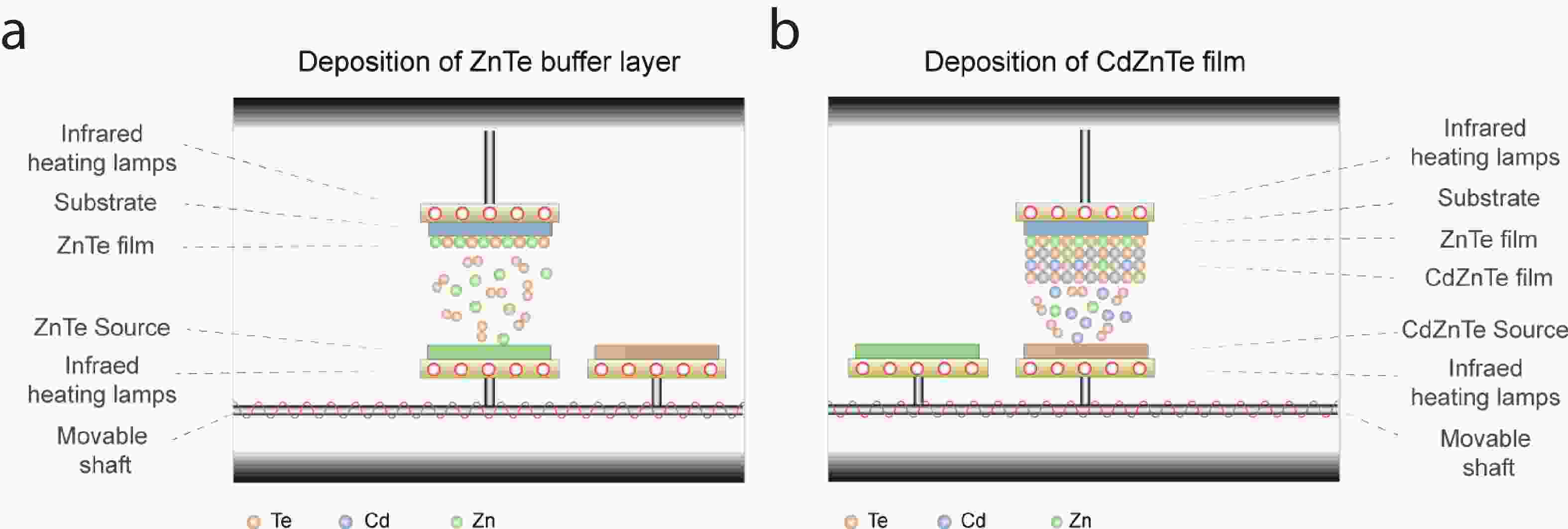
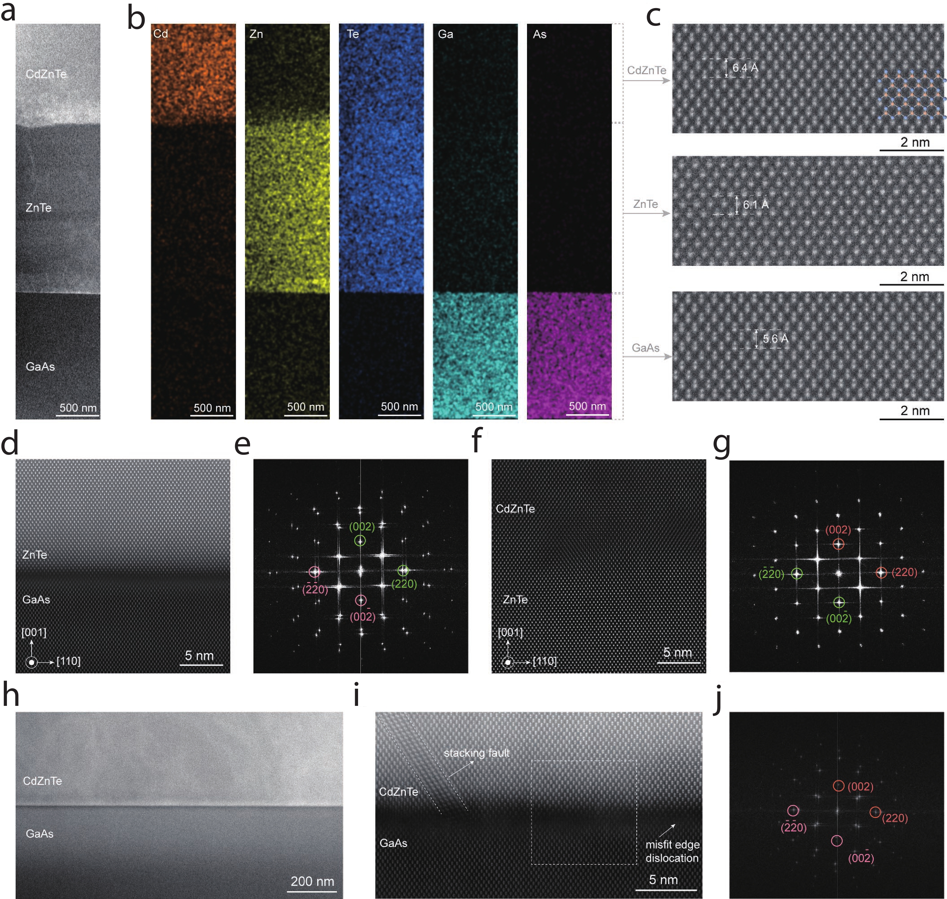
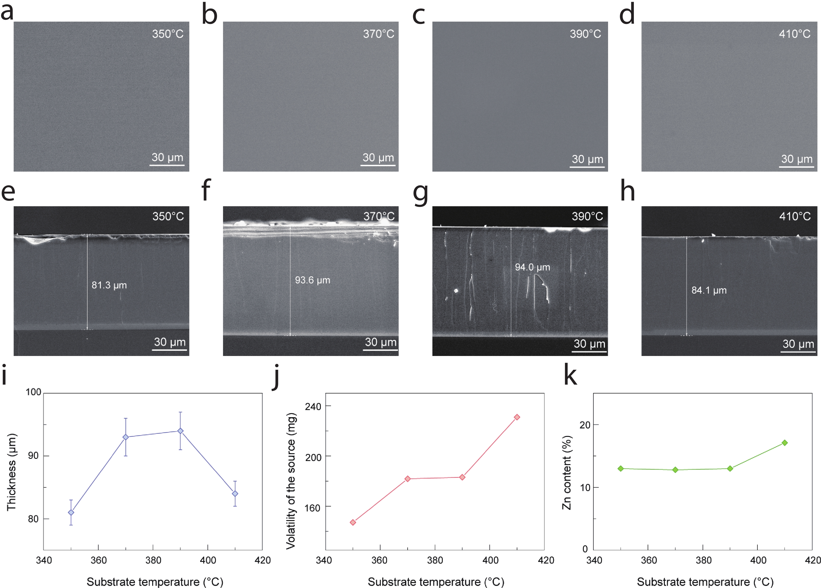
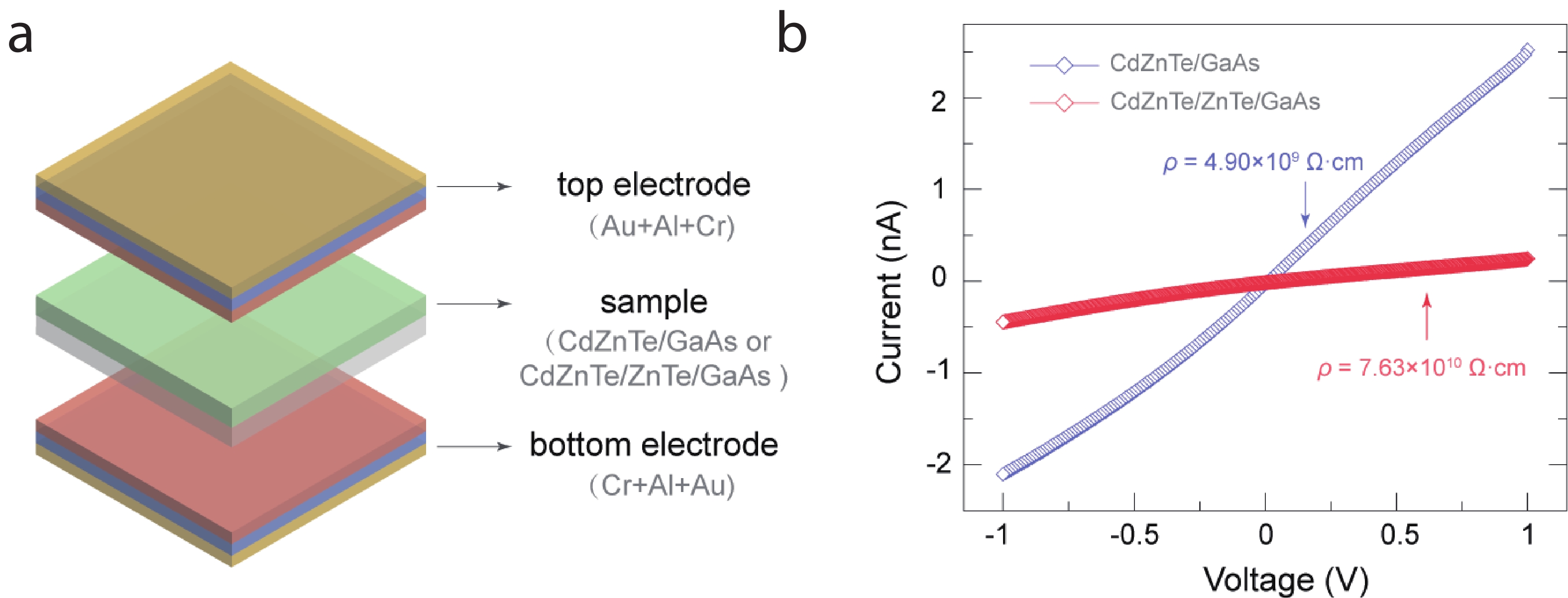
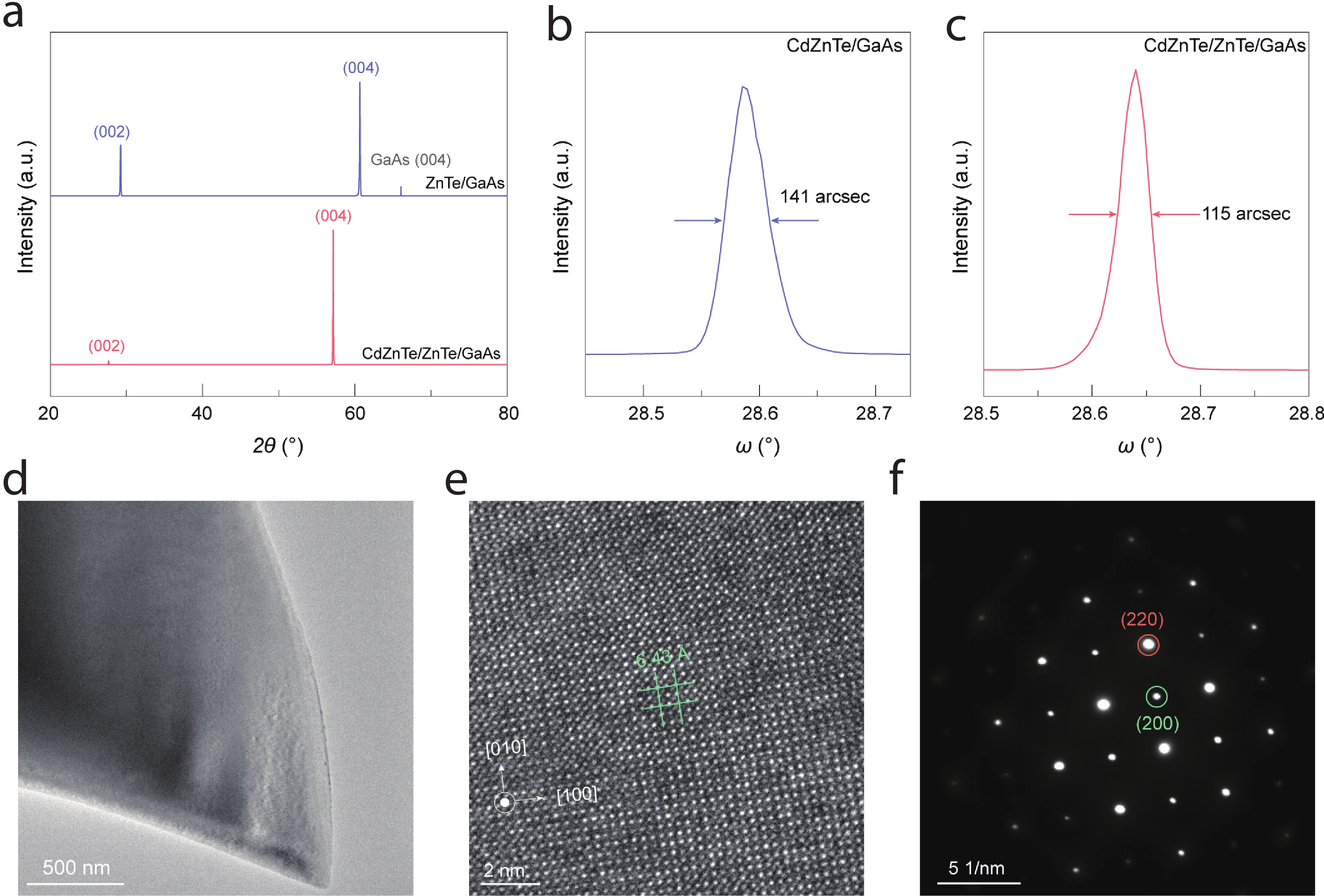
CdZnTe films show great promise for applications in infrared imaging, solar cells, and radiation detection due to their excellent optoelectronic properties. However, single-crystal CdZnTe films directly deposited on commercial GaAs (001) substrate suffer from a high density of crystalline defects caused by a large lattice mismatch. Here we report the epitaxial growth of single-crystal CdZnTe films on GaAs (001) substrate using close spaced sublimation with a single-crystal ZnTe thin film as a buffer layer. As-grown CdZnTe films exhibit higher crystalline quality than those grown without a buffer layer. The optimal substrate temperature range is found to be 370−390  °C, and the growth rate reaches 94 μm/h. This work provides an approach to grow high-quality single-crystal CdZnTe films for optoelectronic device applications.
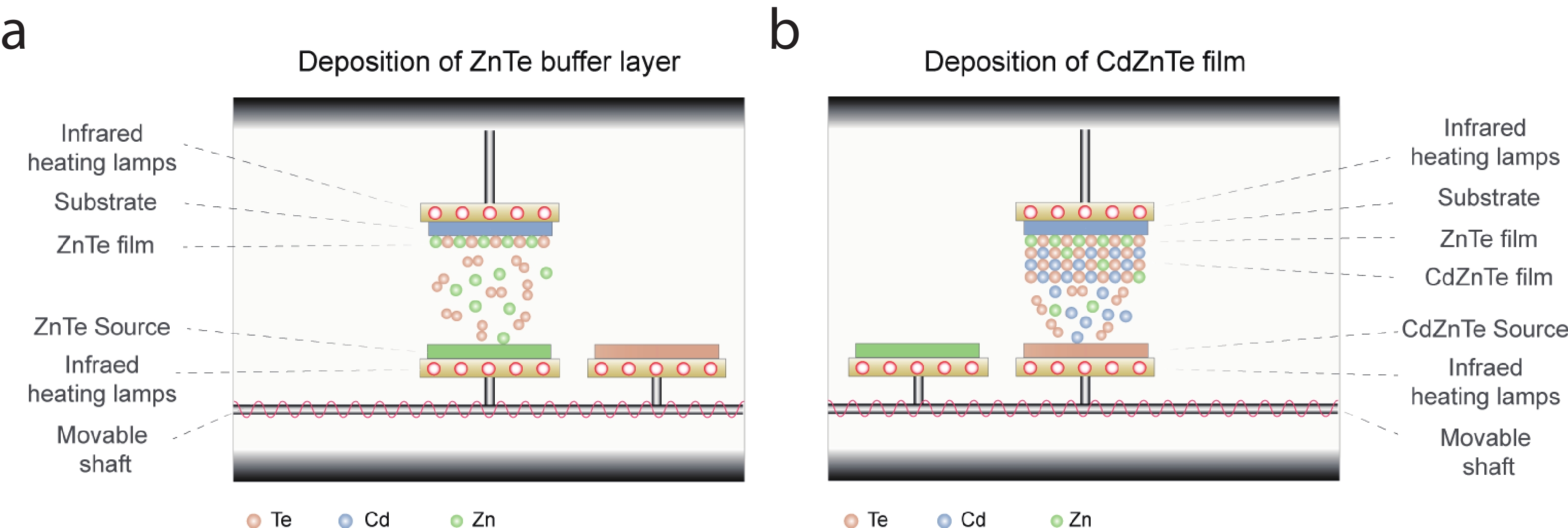
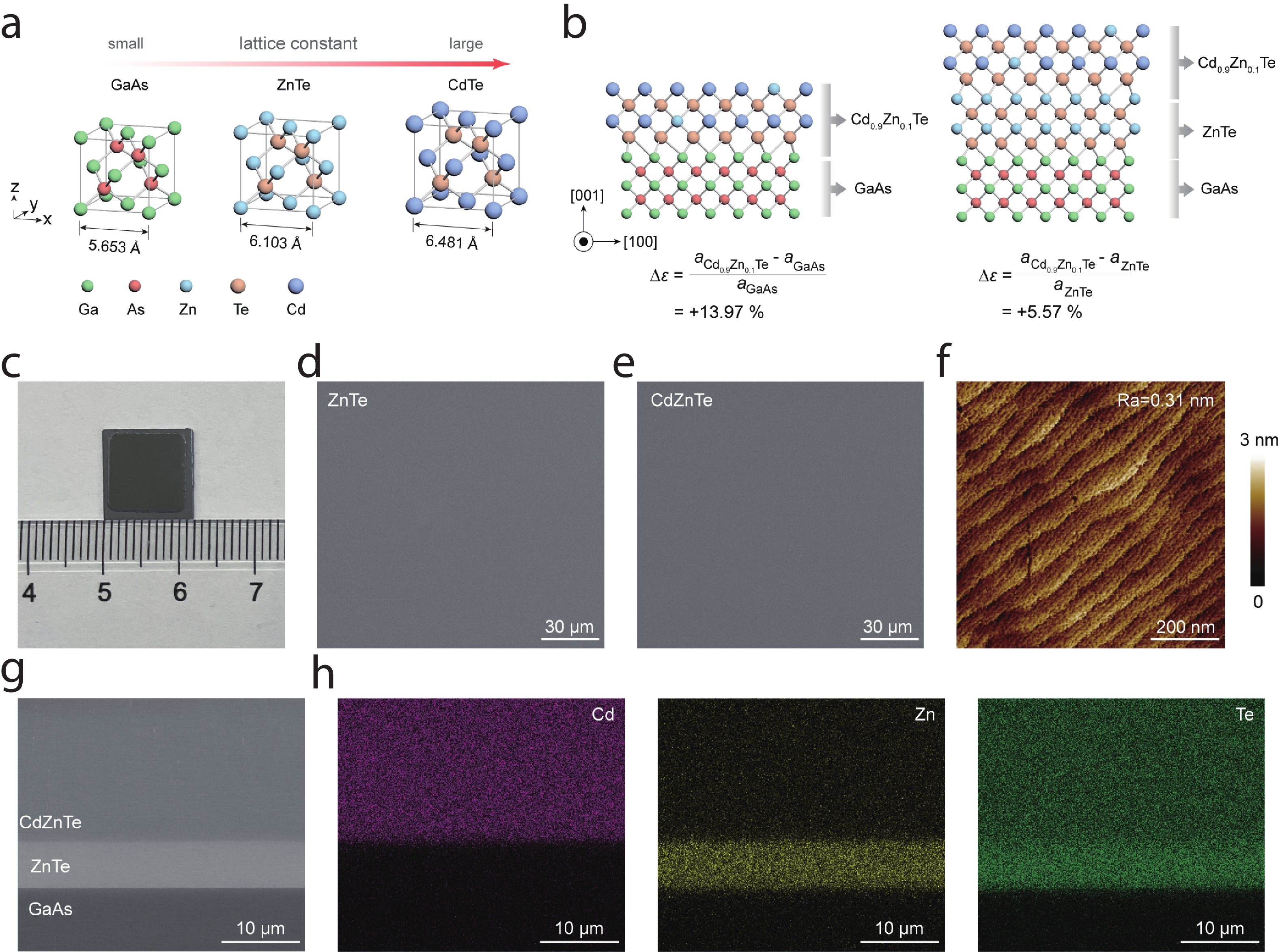
CdZnTe films show great promise for applications in infrared imaging, solar cells, and radiation detection due to their excellent optoelectronic properties. However, single-crystal CdZnTe films directly deposited on commercial GaAs (001) substrate suffer from a high density of crystalline defects caused by a large lattice mismatch. Here we report the epitaxial growth of single-crystal CdZnTe films on GaAs (001) substrate using close spaced sublimation with a single-crystal ZnTe thin film as a buffer layer. As-grown CdZnTe films exhibit higher crystalline quality than those grown without a buffer layer. The optimal substrate temperature range is found to be 370−390  °C, and the growth rate reaches 94 μm/h. This work provides an approach to grow high-quality single-crystal CdZnTe films for optoelectronic device applications.
Ultrathin single-crystalline Bi2S3 nanosheets for high-performance photodetectors
Jintao Gao, Hongyu Liu, Yue Zhang, Zhaoyu Pan, Huanghuang Cheng, Feng Zhuo, Peng Zhang, Songqing Hu, Xuegang Chen, Wenshuai Gao, Xue Liu, Yuxuan Jiang, Jingyue Wang
J. Semicond.  2026, 47(10): 102703  doi: 10.1088/1674-4926/26060011
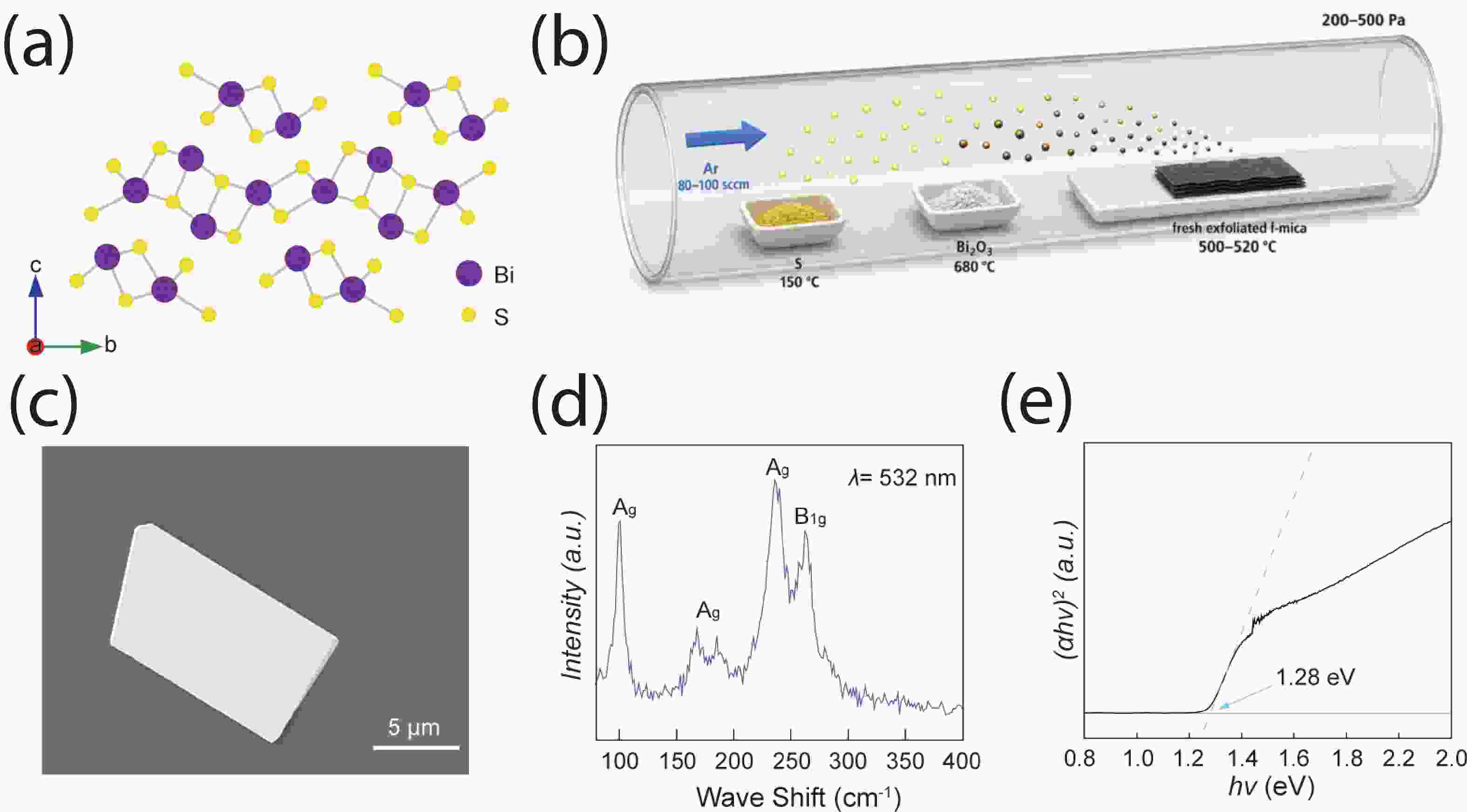
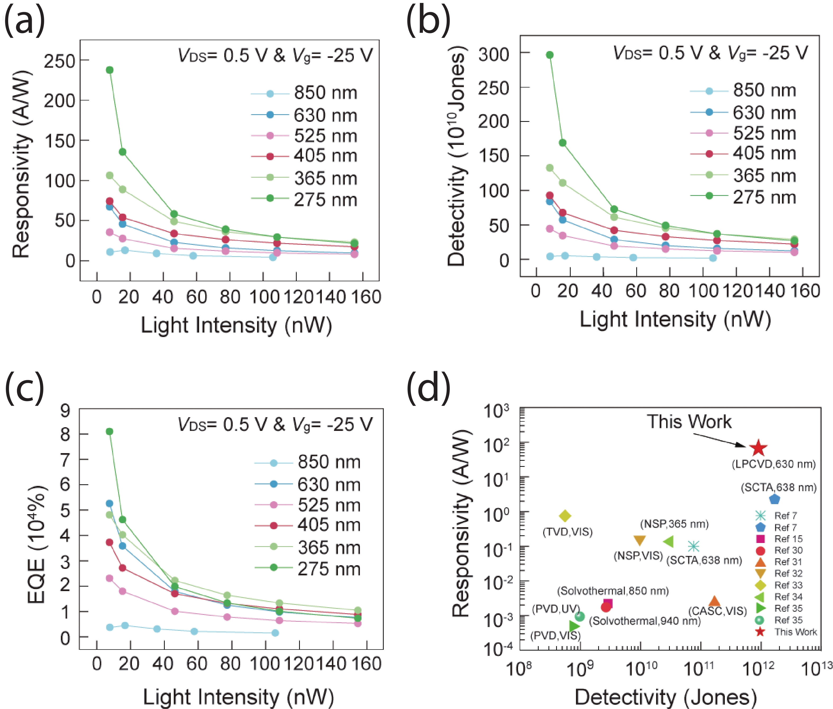
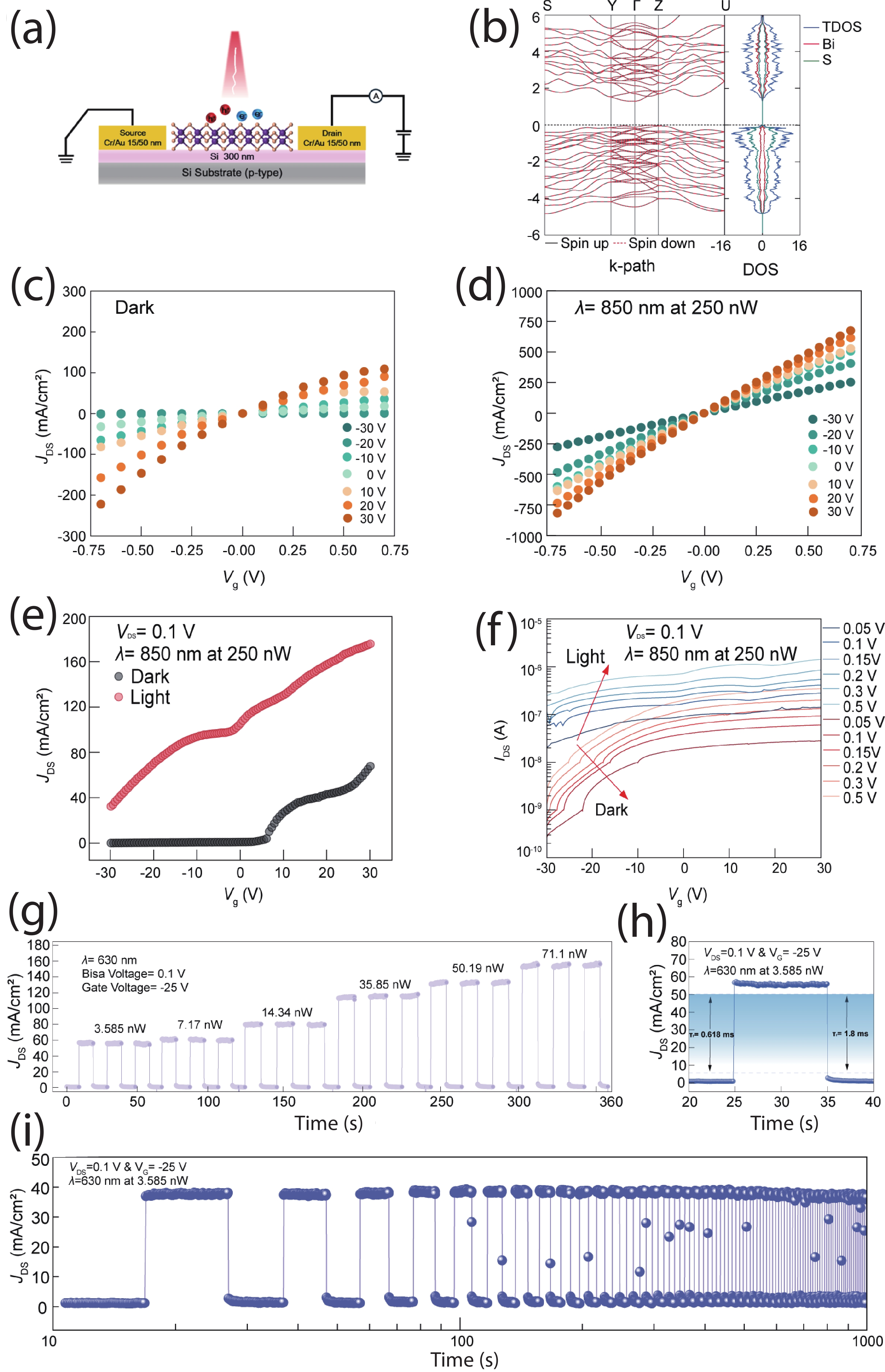
Bismuth sulfide (Bi2S3), a widely studied photocatalytic material, has attracted increasing interest for optoelectronic applications because of its strong light absorption and suitable bandgap. However, the photoelectric properties of single-crystalline Bi2S3 remain insufficiently explored, mainly due to the difficulty in synthesizing high-quality ultrathin crystals suitable for device integration. Here, we report the low-pressure chemical vapor deposition (LPCVD) growth of ultrathin single-crystalline Bi2S3 nanosheets with thicknesses of approximately 40–60 nm and demonstrate high-performance gate-tunable photodetectors based on back-gated field-effect transistor (FET) devices. Under 630 nm illumination, the devices deliver a high responsivity of 67.36 A·W−1, an external quantum efficiency (EQE) of 52618%, and a detectivity on the order of 1012 Jones. These metrics outperform previously reported Bi2S3 photodetection devices and highlight the great potential of LPCVD-grown Bi2S3 for high-speed and high-sensitivity photodetection. Combined with its tunable bandgap and structural anisotropy, Bi2S3 represents a promising material platform for next-generation photodetectors, image sensors and integrated optoelectronic technologies.
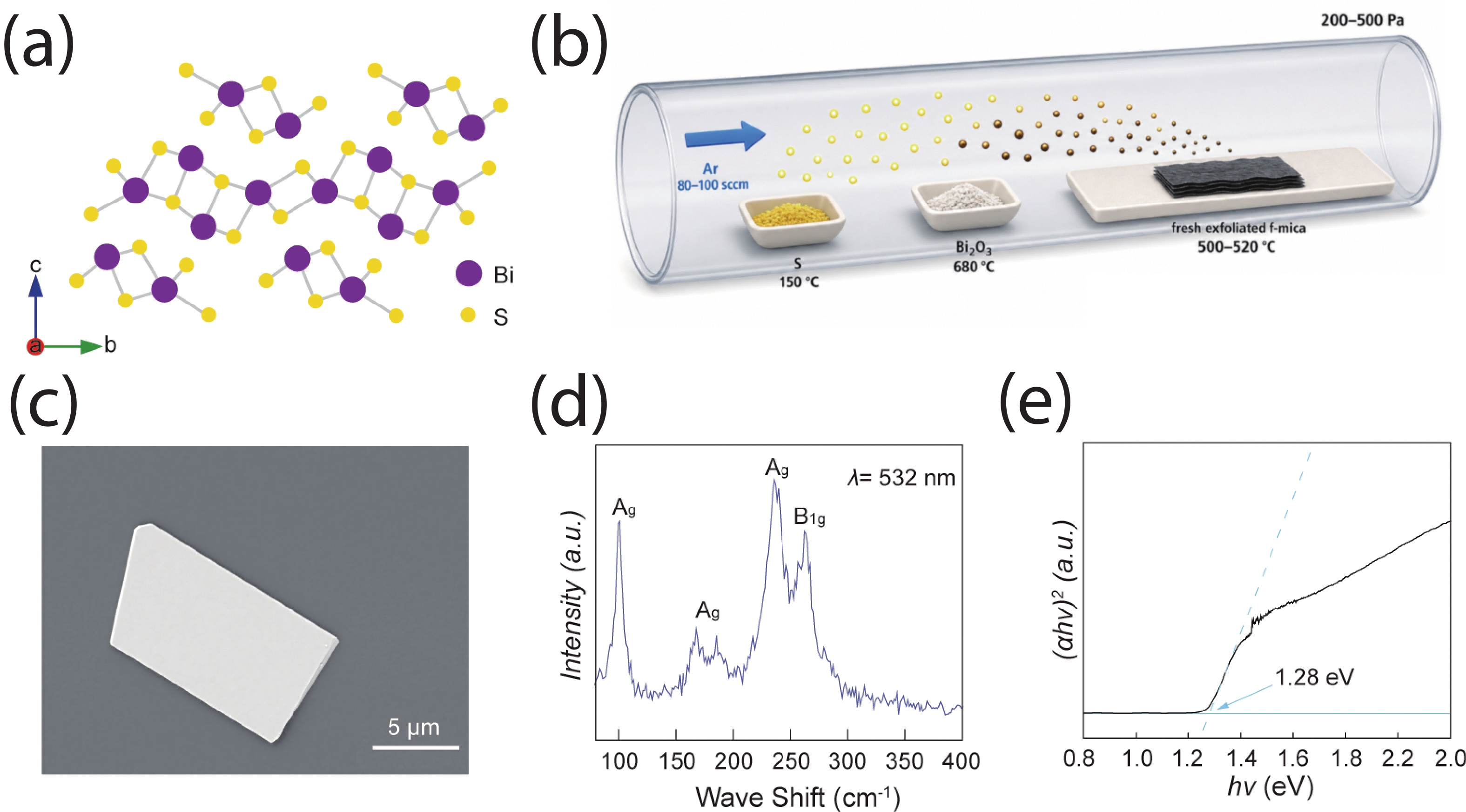
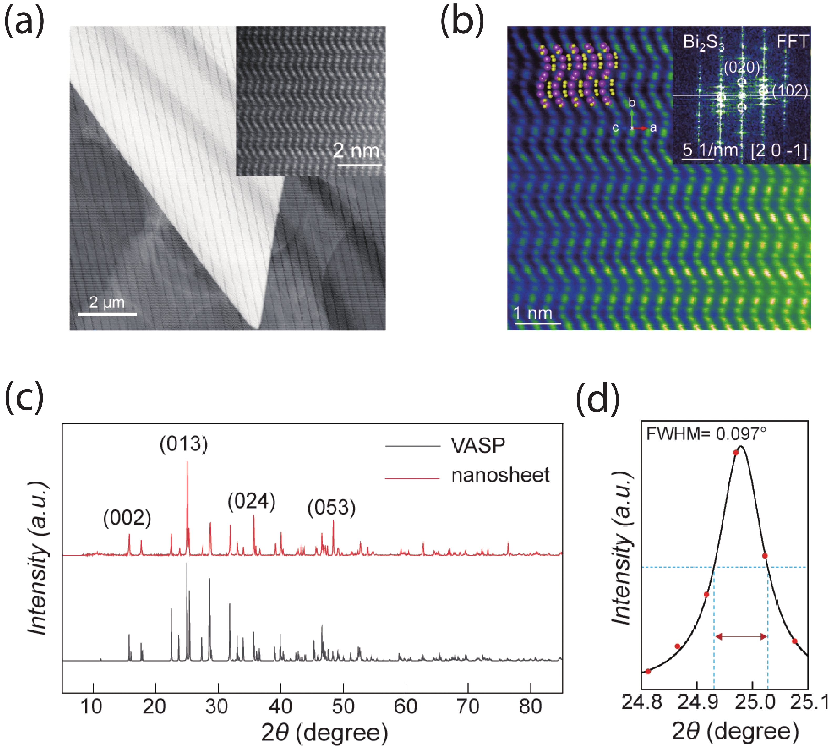
Bismuth sulfide (Bi2S3), a widely studied photocatalytic material, has attracted increasing interest for optoelectronic applications because of its strong light absorption and suitable bandgap. However, the photoelectric properties of single-crystalline Bi2S3 remain insufficiently explored, mainly due to the difficulty in synthesizing high-quality ultrathin crystals suitable for device integration. Here, we report the low-pressure chemical vapor deposition (LPCVD) growth of ultrathin single-crystalline Bi2S3 nanosheets with thicknesses of approximately 40–60 nm and demonstrate high-performance gate-tunable photodetectors based on back-gated field-effect transistor (FET) devices. Under 630 nm illumination, the devices deliver a high responsivity of 67.36 A·W−1, an external quantum efficiency (EQE) of 52618%, and a detectivity on the order of 1012 Jones. These metrics outperform previously reported Bi2S3 photodetection devices and highlight the great potential of LPCVD-grown Bi2S3 for high-speed and high-sensitivity photodetection. Combined with its tunable bandgap and structural anisotropy, Bi2S3 represents a promising material platform for next-generation photodetectors, image sensors and integrated optoelectronic technologies.
Low-temperature growth of high-quality Bi2O2Se for high-performance photodetection
Xiu Liu, Hengrui Fu, Tiange Zhao, Yiye Yu, Yuzhuo Bai, Xun Ge, Xiaoting Wang
J. Semicond.  2026, 47(10): 102704  doi: 10.1088/1674-4926/26060015
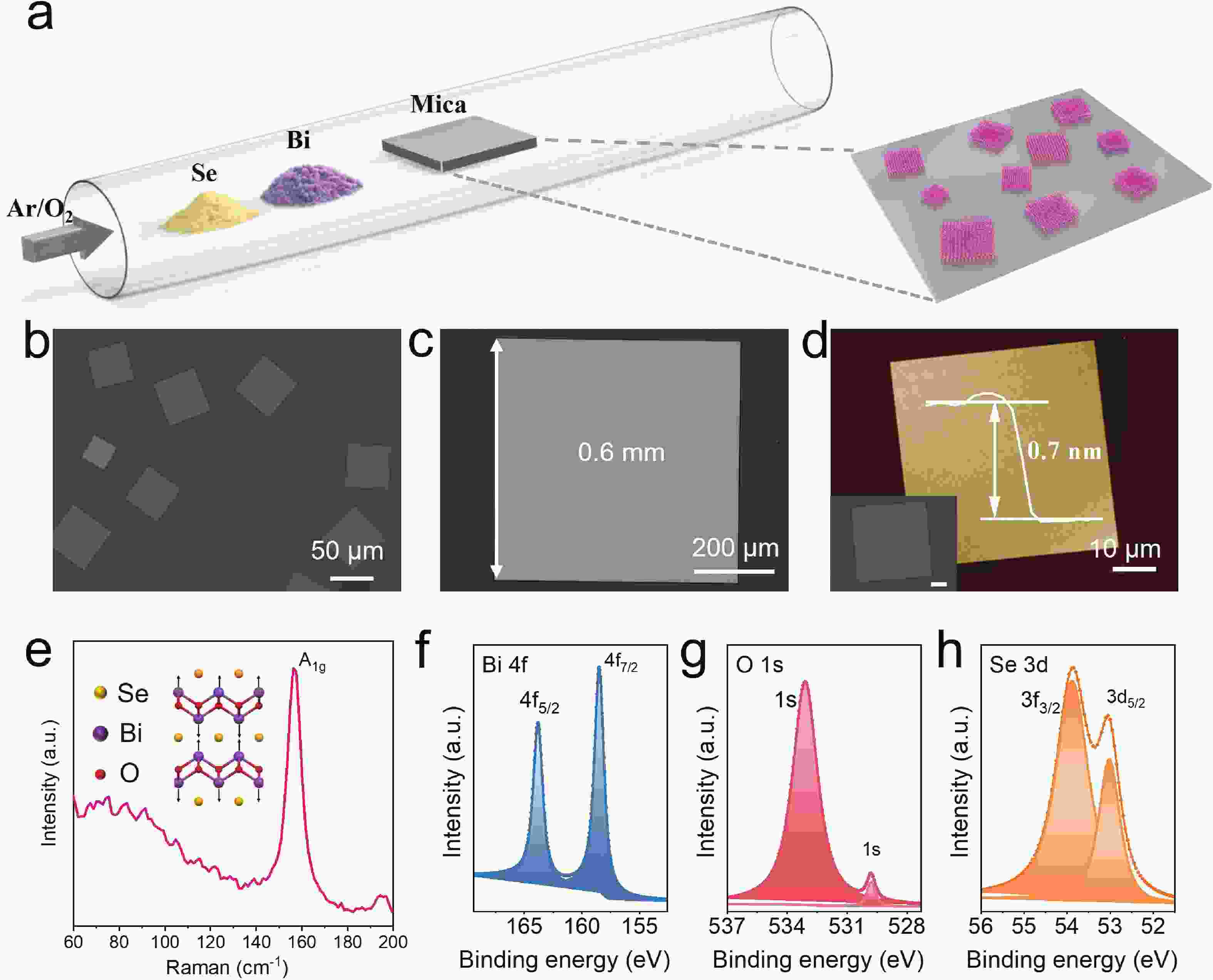
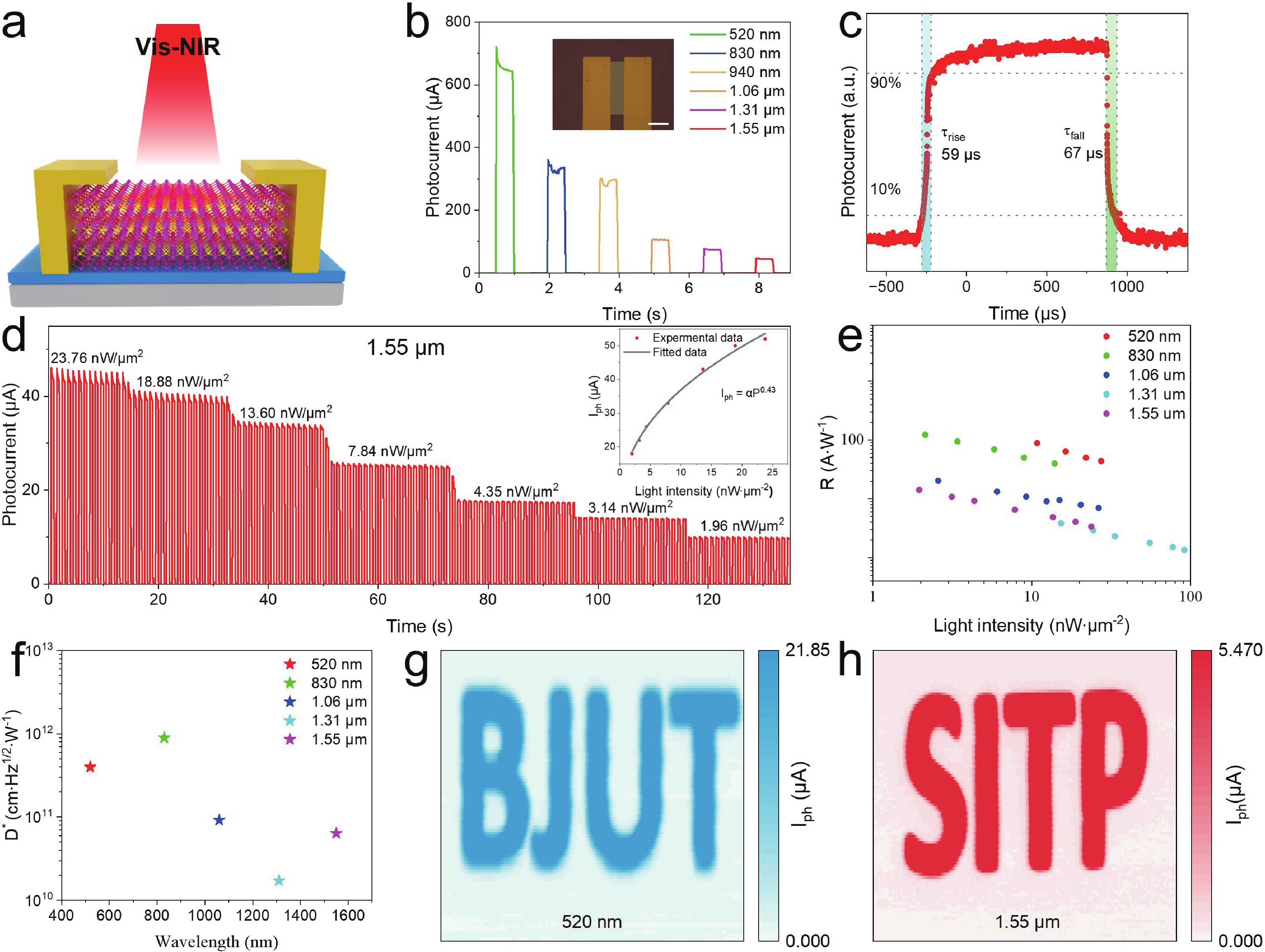
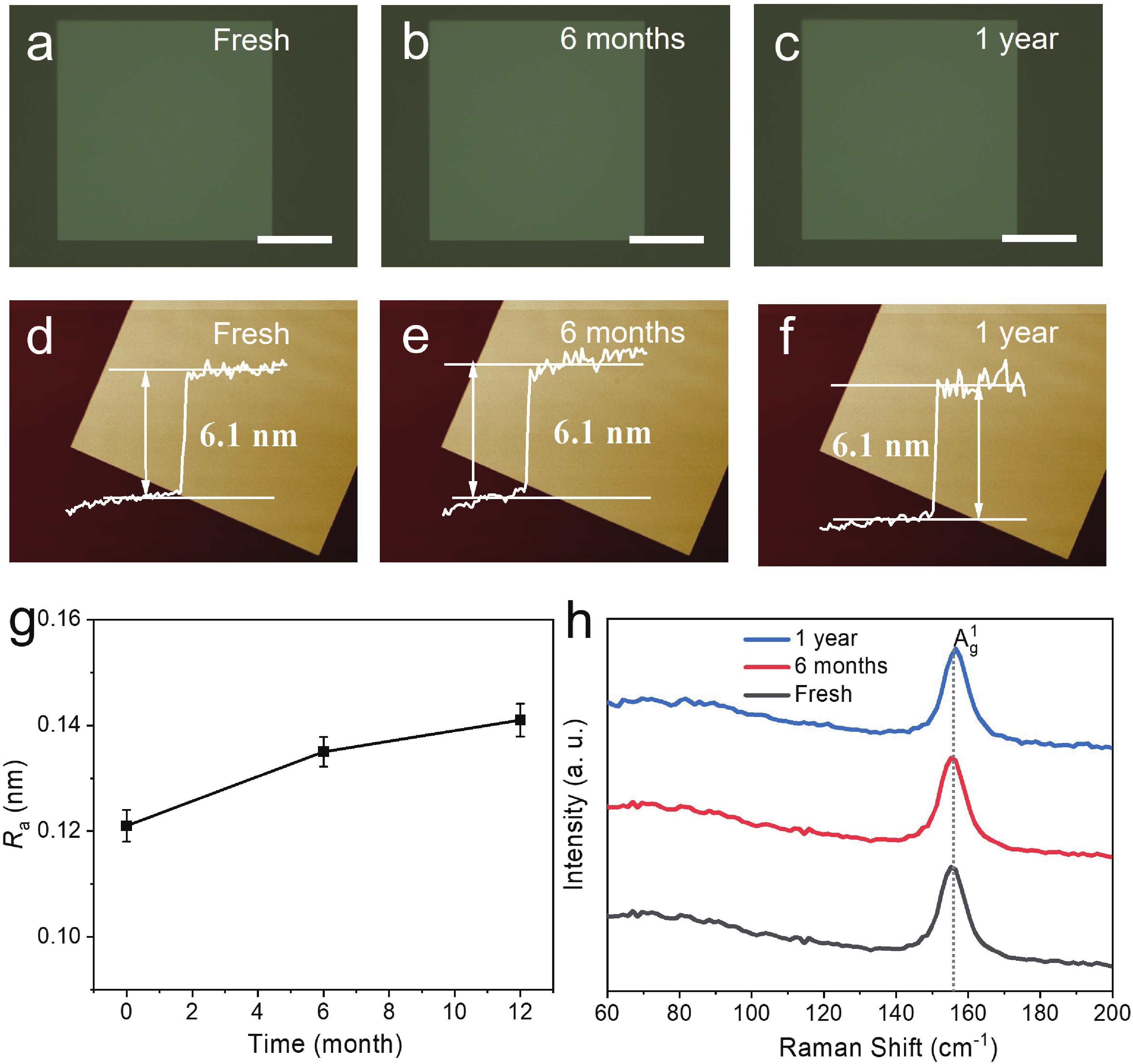
Bi2O2Se is a high-mobility, narrow-bandgap n-type layered semiconductor promising for broadband photodetection. However, its synthesis often relies on high temperatures or complex precursor systems that increase the thermal budget and limit device integration. Here we report a low-melting-point precursor-assisted chemical vapor deposition (CVD) strategy for growing high-quality Bi2O2Se nanosheets at 450 °C. Using elemental Bi and Se powders under an Ar/O2 atmosphere, we obtain single-crystalline nanosheets with uniform composition, long-term air stability and lateral sizes up to 0.6 mm. Photodetectors fabricated from the nanosheets show broadband response from 520 to 1550 nm, with a responsivity of 14.17 A∙W−1 and a specific detectivity of 6.39 × 10¹⁰ Jones at 1550 nm. The devices also exhibit fast response, with rise and fall times of 59 and 67 μs, respectively. Single-pixel imaging at 520 and 1550 nm further demonstrates their visible and near-infrared imaging capability. This work establishes low-melting-point precursor-assisted CVD as an effective route for low-temperature Bi2O2Se growth and points to its potential in broadband, high-speed photodetection.
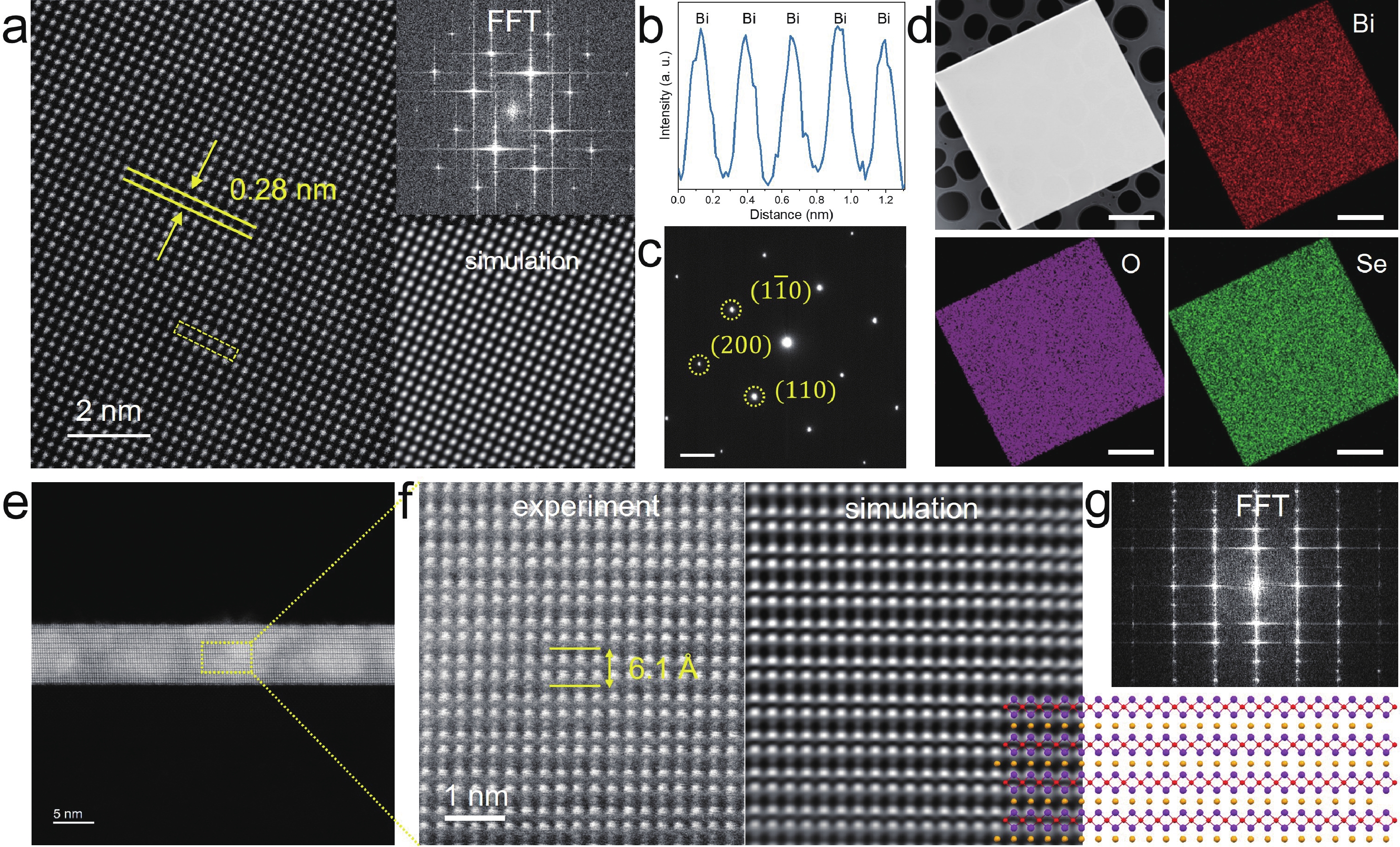
Bi2O2Se is a high-mobility, narrow-bandgap n-type layered semiconductor promising for broadband photodetection. However, its synthesis often relies on high temperatures or complex precursor systems that increase the thermal budget and limit device integration. Here we report a low-melting-point precursor-assisted chemical vapor deposition (CVD) strategy for growing high-quality Bi2O2Se nanosheets at 450 °C. Using elemental Bi and Se powders under an Ar/O2 atmosphere, we obtain single-crystalline nanosheets with uniform composition, long-term air stability and lateral sizes up to 0.6 mm. Photodetectors fabricated from the nanosheets show broadband response from 520 to 1550 nm, with a responsivity of 14.17 A∙W−1 and a specific detectivity of 6.39 × 10¹⁰ Jones at 1550 nm. The devices also exhibit fast response, with rise and fall times of 59 and 67 μs, respectively. Single-pixel imaging at 520 and 1550 nm further demonstrates their visible and near-infrared imaging capability. This work establishes low-melting-point precursor-assisted CVD as an effective route for low-temperature Bi2O2Se growth and points to its potential in broadband, high-speed photodetection.
In situ visualized synthesis of two-dimensional MoS2 with tunable metal-to-semiconductor transition
Sheng Guo, Tiefeng Yang, Manyan Xie, Ziyi Huang, Hanrong Xie, Miao Liu, Zitong Liu, Haoran Guo, Rui Rong, Chui Pian, Ziliang Fang, Zhen Wang, Heyuan Guan, Huihui Lu
J. Semicond.  2026, 47(10): 102705  doi: 10.1088/1674-4926/26060017
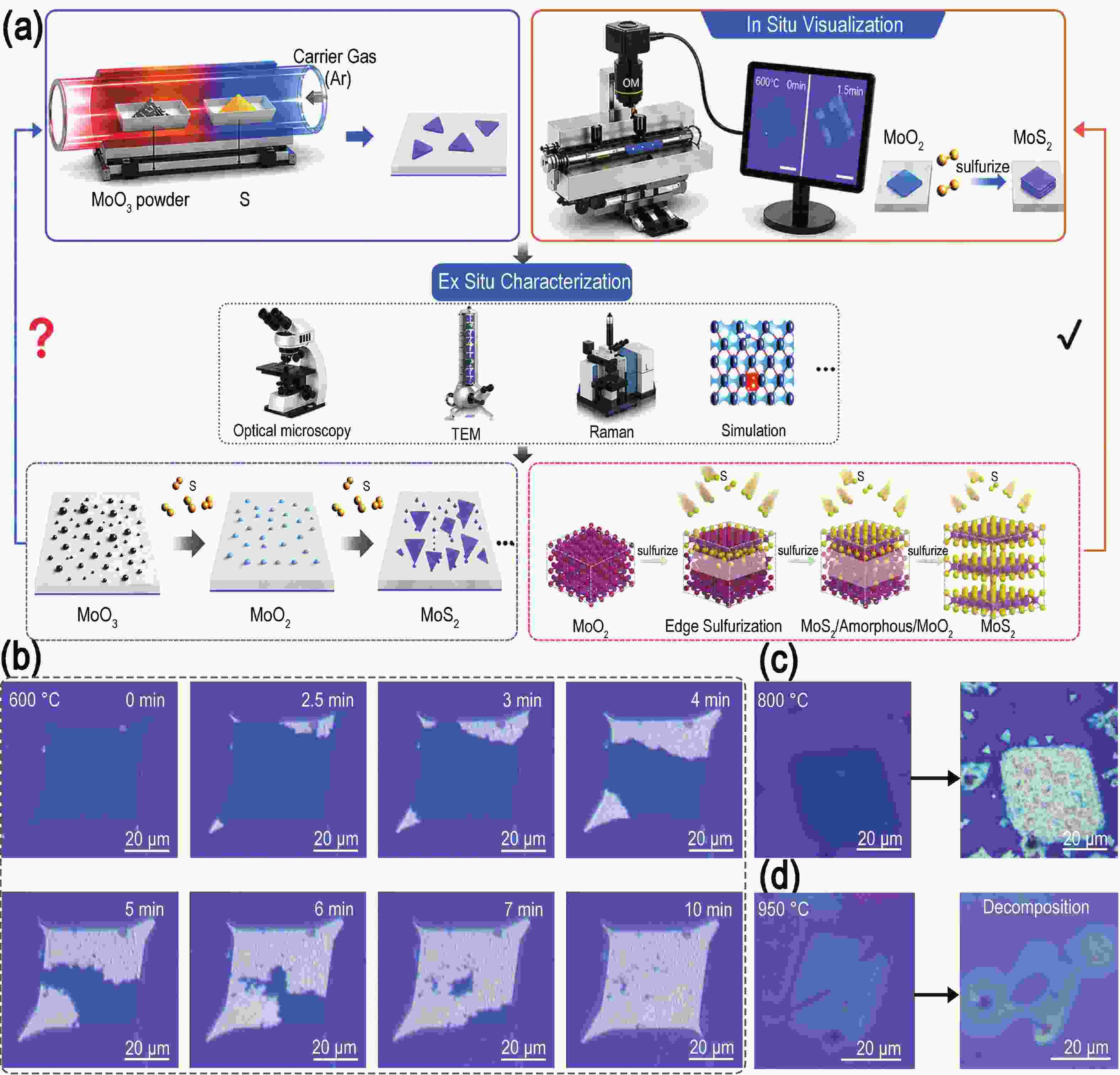
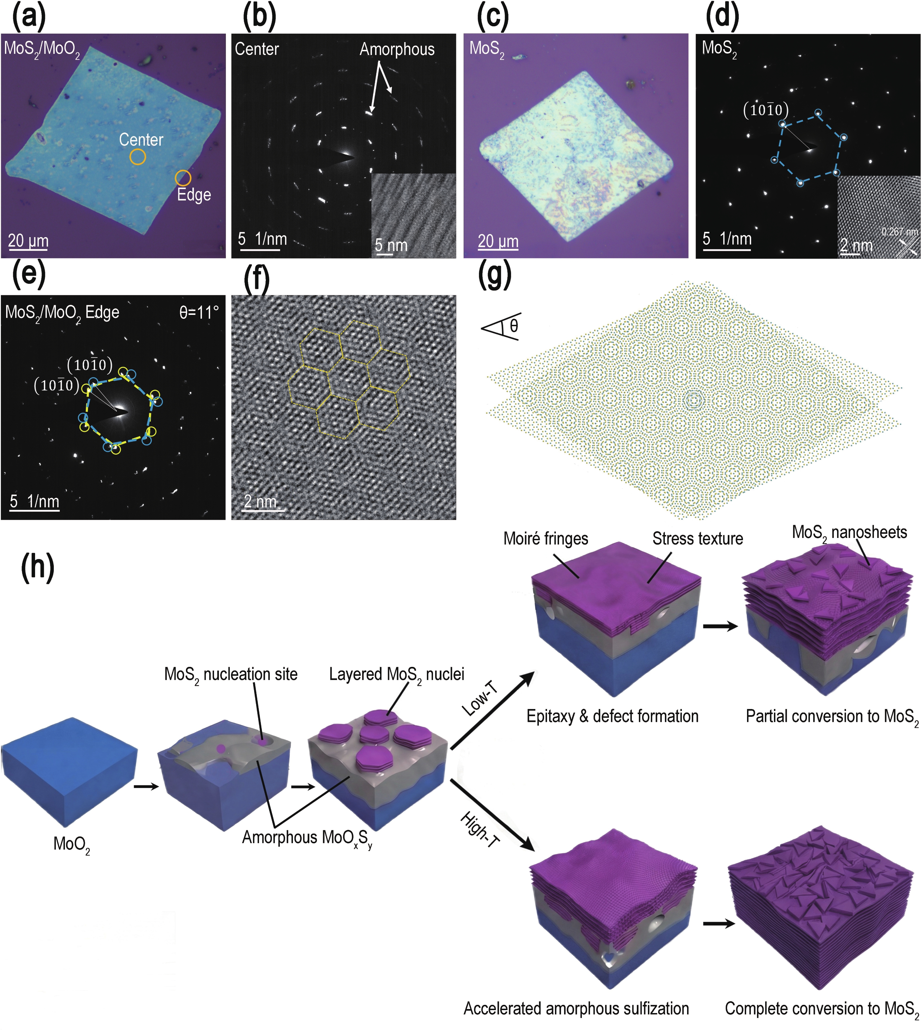
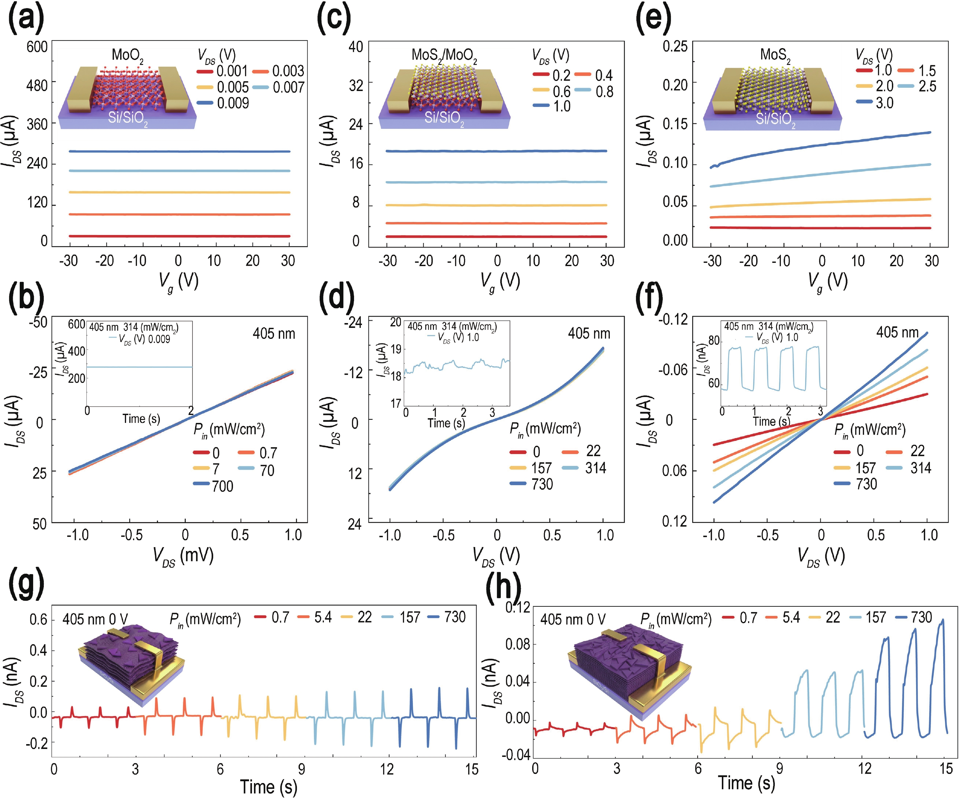
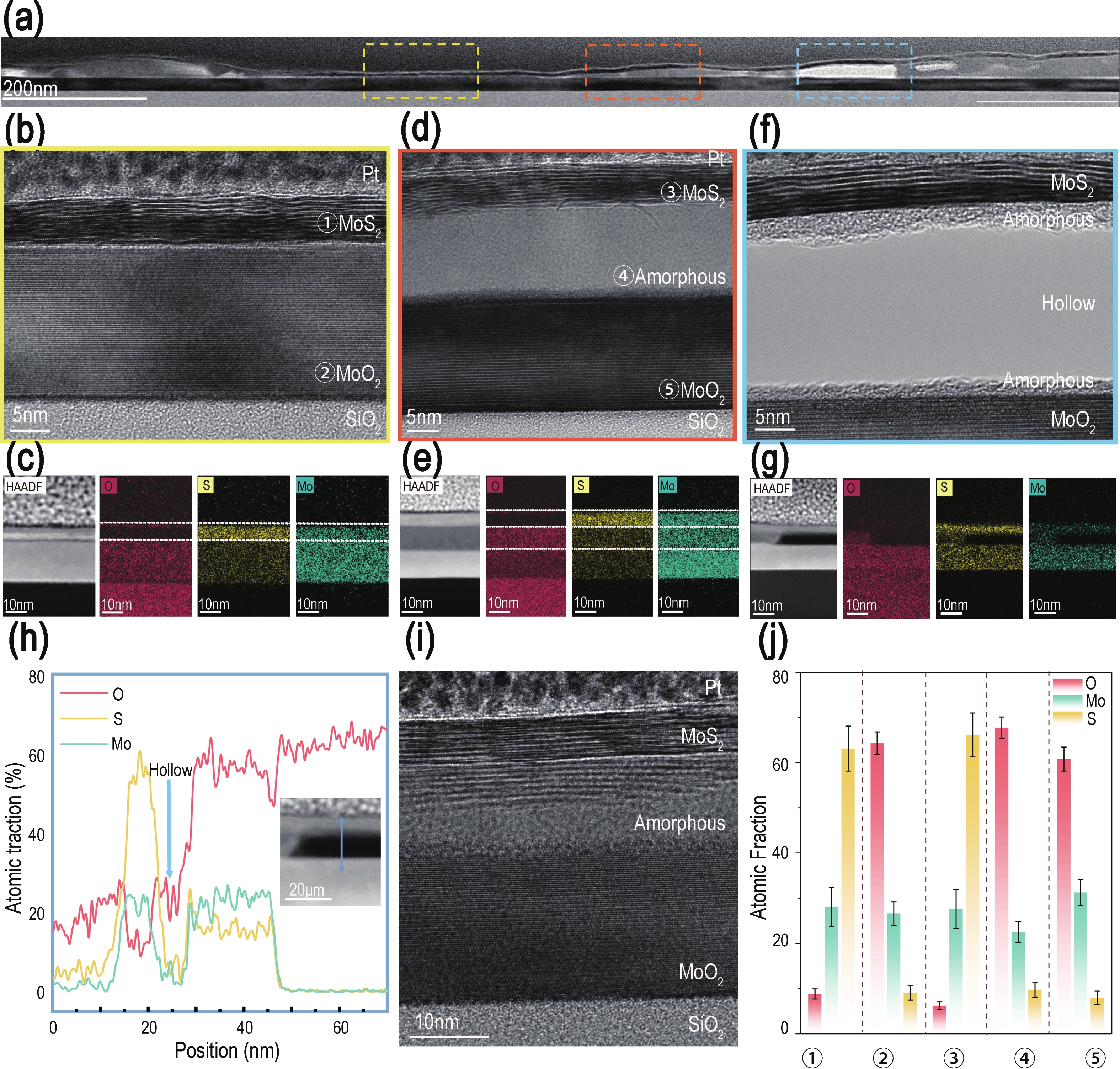
Visualizing the growth of two-dimensional materials is crucial for clarifying growth mechanisms and enabling controllable synthesis. Recent in situ electron microscopy has captured atomic-scale images of MoS2 growth, extending studies beyond post-growth characterization and theoretical simulations. Yet it remains unclear whether behavior observed under the demanding conditions of transmission electron microscopy and low vapor pressure applies to macroscopic vapor-phase synthesis. Here, we use in situ optical microscopy, Raman spectroscopy, electron microscopy, and device measurements to track the complete temperature-dependent conversion pathway of two-dimensional MoO2 nanosheets into MoS2 during sulfurization. The transformation is not a direct one-step phase transition. Rather, it follows a multistep pathway involving surface nucleation, formation of an amorphous Mo−S−O intermediate, local structural ordering, and final crystallization into layered MoS2. Partially sulfurized samples retain structural asymmetry, including an intermediate phase, voids, strain, and moiré fringes, while fully sulfurized samples form uniform layered crystals. Device measurements show that this structural evolution is accompanied by a transport transition from metallic MoO2 to semiconducting MoS2. Moreover, exfoliated MoS2 from partially sulfurized samples preserves local asymmetry and exhibits a pronounced pyroelectric effect under illumination, linking the conversion pathway with optoelectronic functionality.
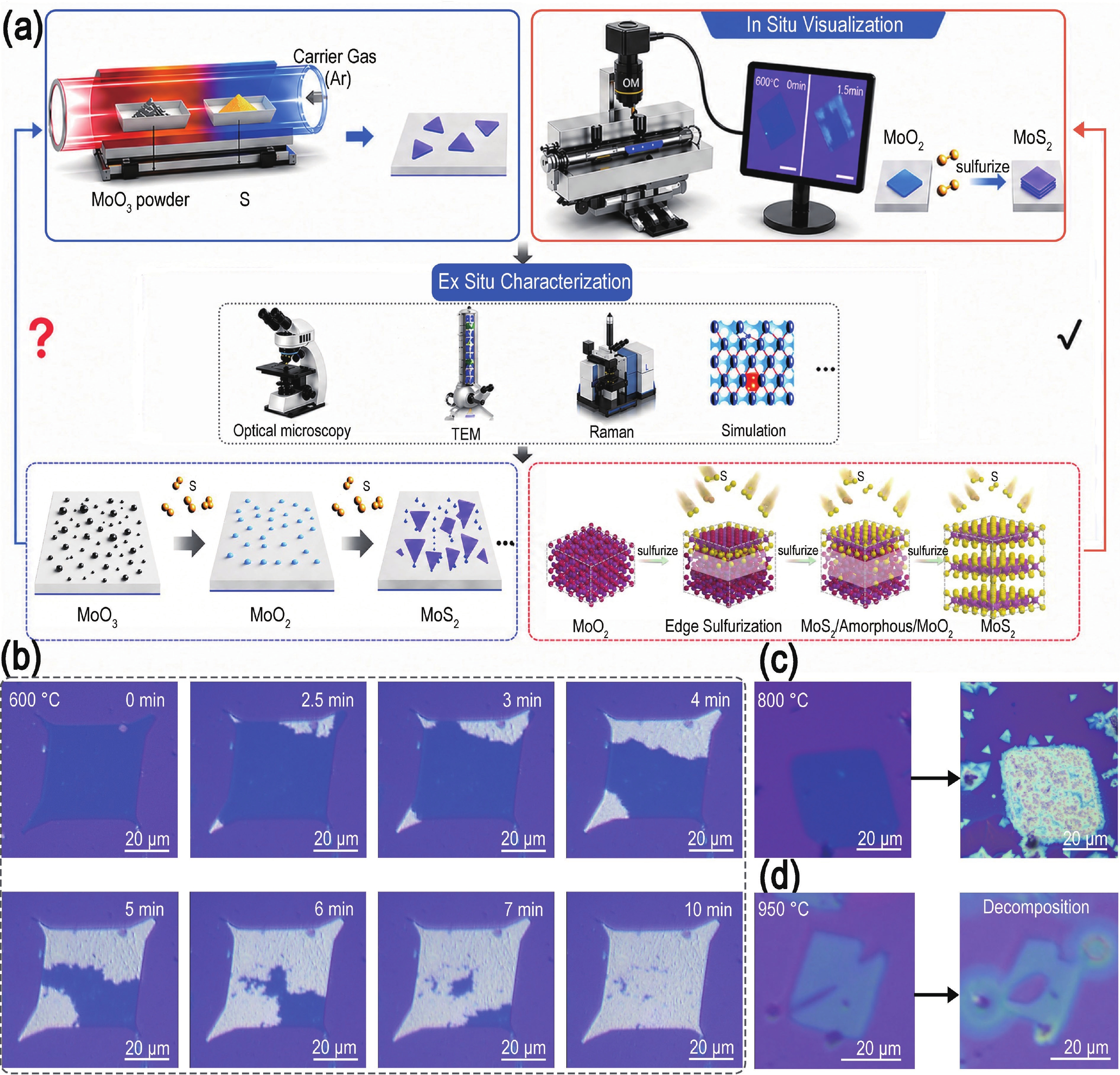
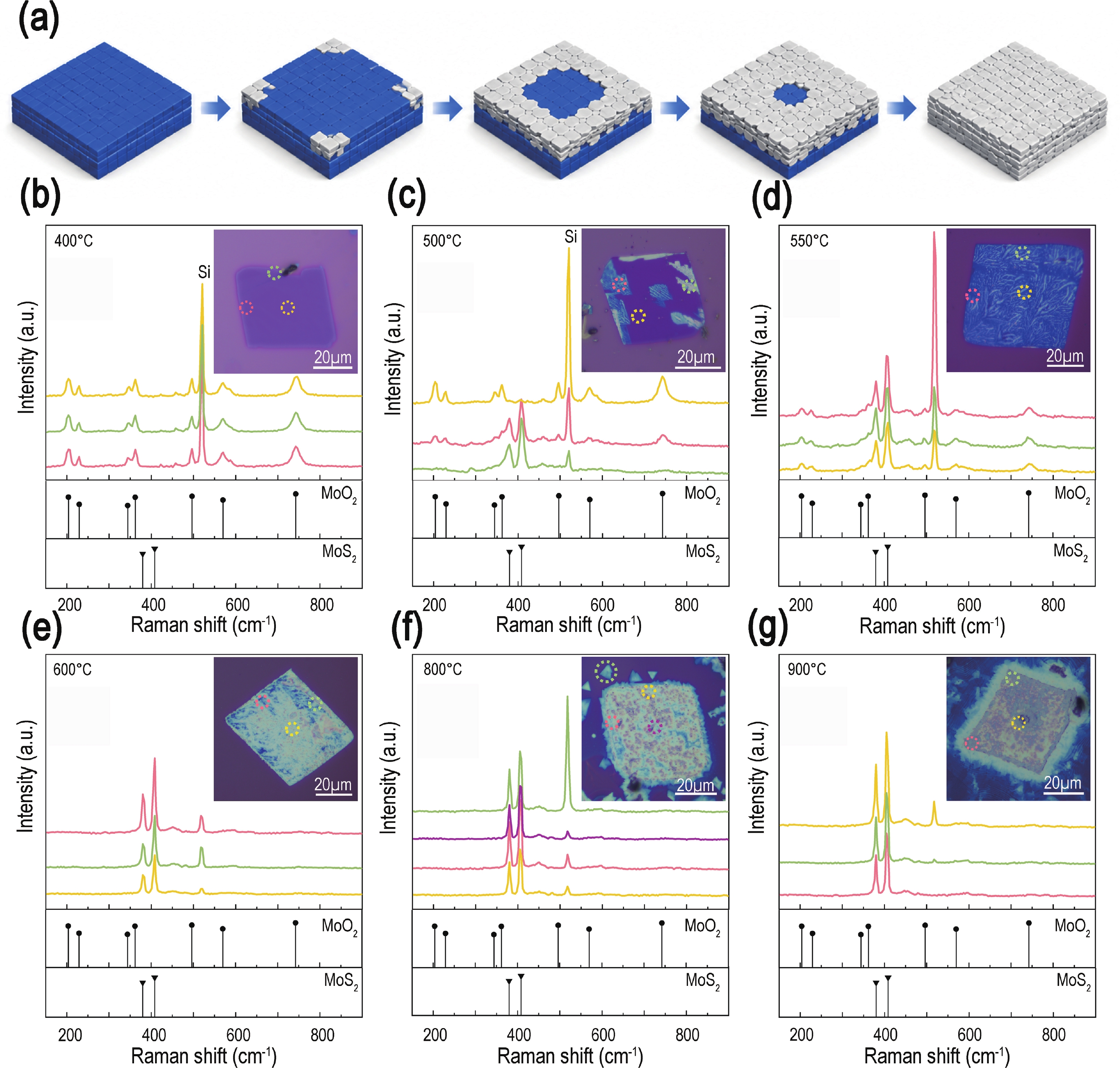
Visualizing the growth of two-dimensional materials is crucial for clarifying growth mechanisms and enabling controllable synthesis. Recent in situ electron microscopy has captured atomic-scale images of MoS2 growth, extending studies beyond post-growth characterization and theoretical simulations. Yet it remains unclear whether behavior observed under the demanding conditions of transmission electron microscopy and low vapor pressure applies to macroscopic vapor-phase synthesis. Here, we use in situ optical microscopy, Raman spectroscopy, electron microscopy, and device measurements to track the complete temperature-dependent conversion pathway of two-dimensional MoO2 nanosheets into MoS2 during sulfurization. The transformation is not a direct one-step phase transition. Rather, it follows a multistep pathway involving surface nucleation, formation of an amorphous Mo−S−O intermediate, local structural ordering, and final crystallization into layered MoS2. Partially sulfurized samples retain structural asymmetry, including an intermediate phase, voids, strain, and moiré fringes, while fully sulfurized samples form uniform layered crystals. Device measurements show that this structural evolution is accompanied by a transport transition from metallic MoO2 to semiconducting MoS2. Moreover, exfoliated MoS2 from partially sulfurized samples preserves local asymmetry and exhibits a pronounced pyroelectric effect under illumination, linking the conversion pathway with optoelectronic functionality.
Anomalous gate-tunable capacitance in Van der Waals heterostructures
Linshang Chen, Haoran Long, Heng Wu, Rui Mei, Zhengyu Su, Mengjie Feng, Jiang-Bin Wu, Kenji Watanabe, Takashi Taniguchi, Xuewei Cao, Zhongming Wei, Ping-Heng Tan, Yanmeng Shi
J. Semicond.  2026, 47(10): 102706  doi: 10.1088/1674-4926/26040034
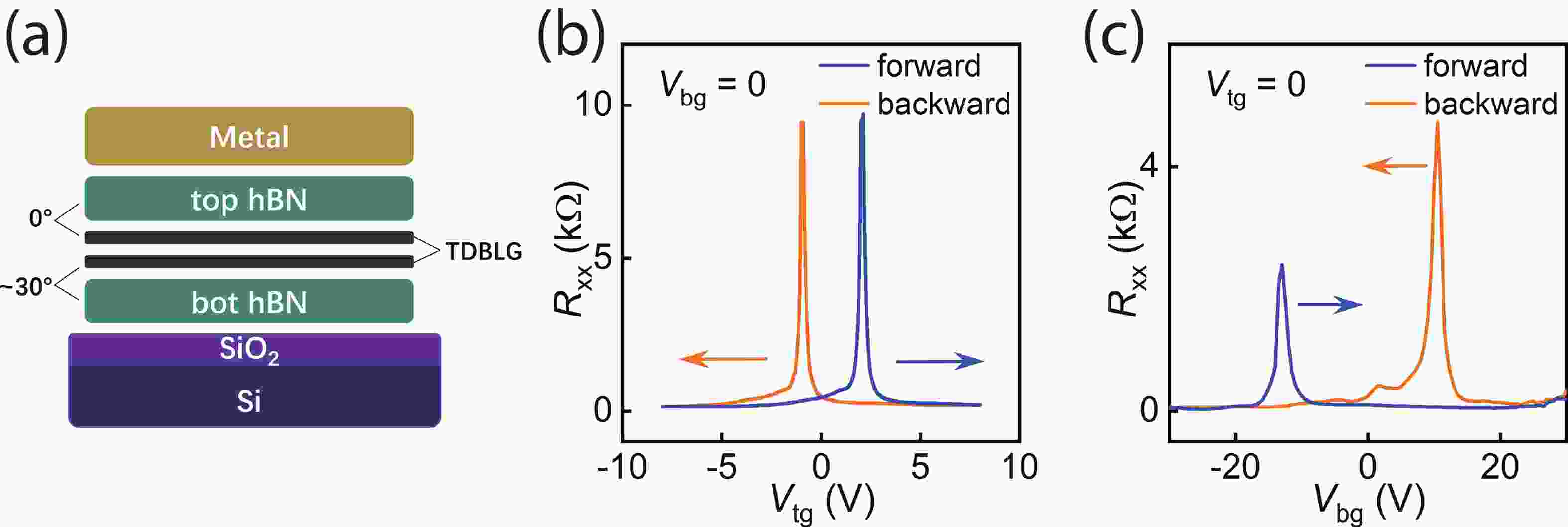
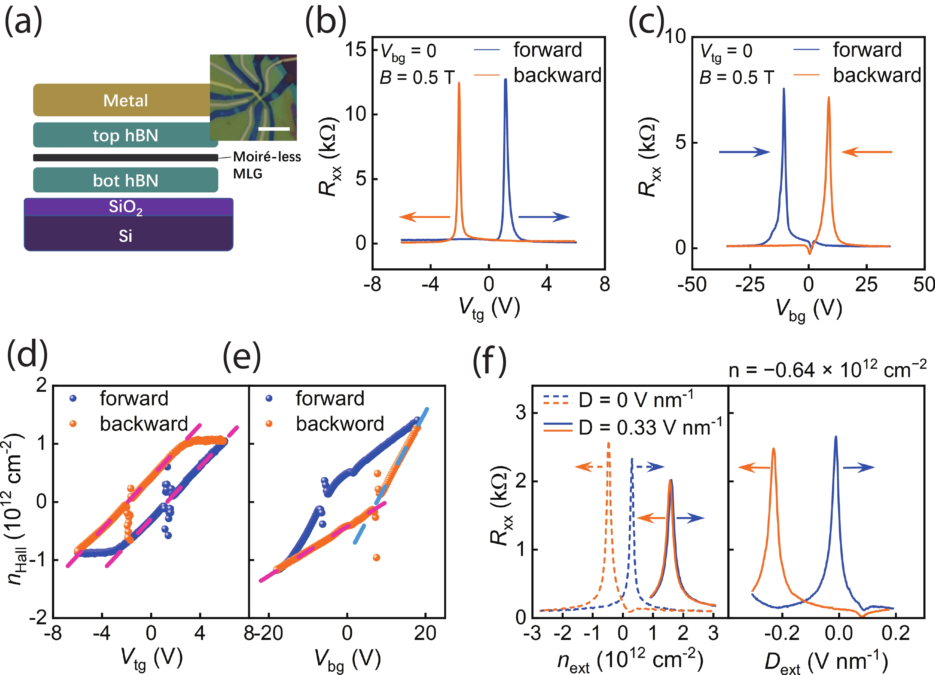
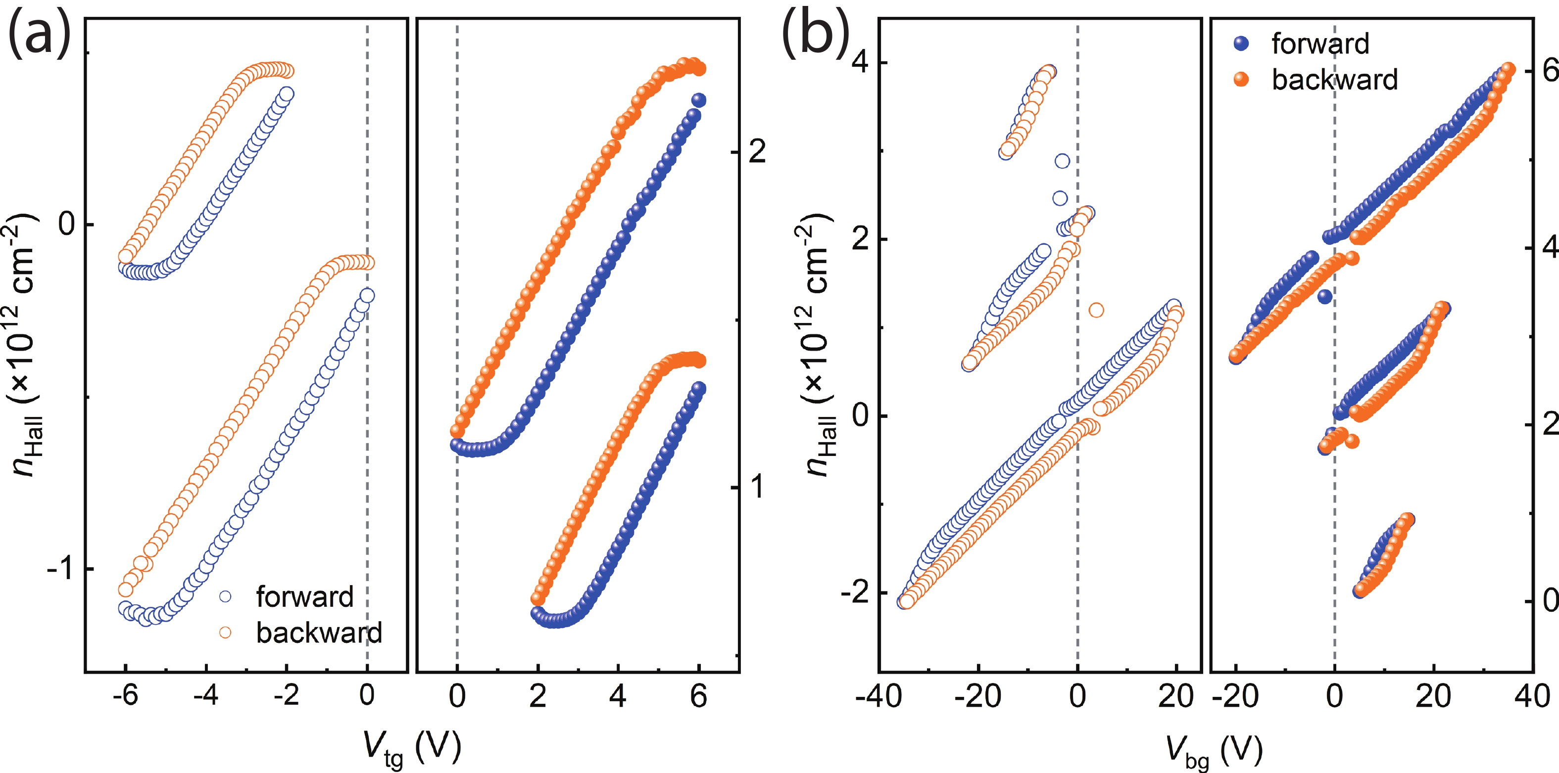
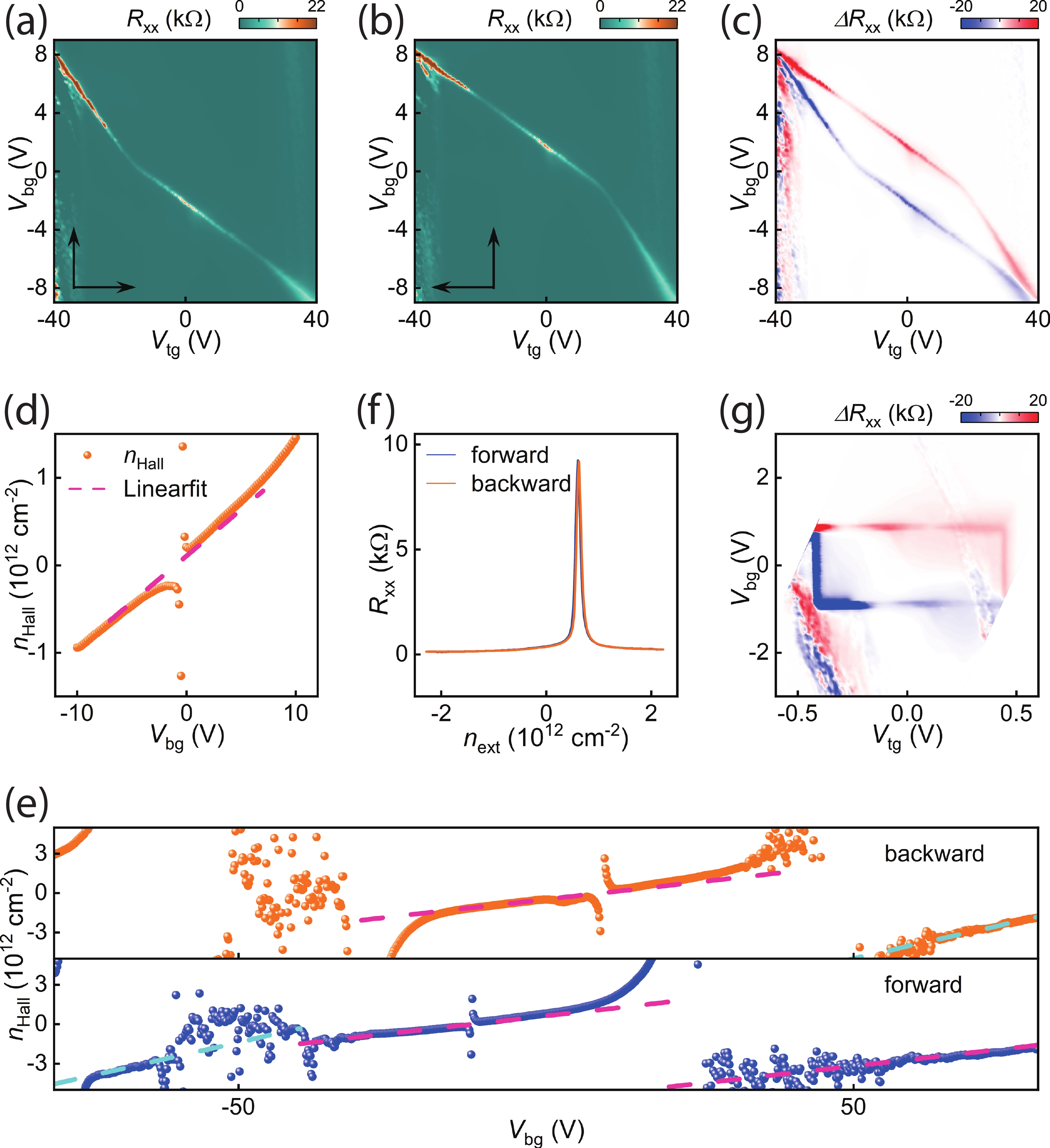
The ferroelectricity emerging in non-polar graphene/hexagonal boron nitride (hBN) heterostructures has drawn considerable attention because of its fascinating properties and promising high-frequency electrical polarization switching. Yet, the underlying mechanism is still under debate. Here in twisted double bilayer graphene (TDBLG) aligned with its neighboring hBN, we observed two types of hysteresis-delayed hysteresis in top gate induced by the anomalous screening, and advanced hysteresis in back gate caused by the anomalous gate-tunable capacitance. To investigate the role played by moiré potential in the anomalous hysteresis, we studied a moiréless graphene heterostructure. Unexpectedly, we observed exactly the same phenomena in this control device. Our findings suggest that the anomalous ferroelectricity in graphene/hBN heterostructures may originate from the dielectric material hBN, calling for further structural investigations on hBN. Further analysis indicates that those hysteresis can be asymmetric and scalable with applied external electric fields, distinct from conventional ferroelectric switching with well-defined coercive fields. The observation of gate-tunable capacitance provides more insights in the mysterious ferroelectricity in graphene/hBN heterostructures, and should enable new design of memory devices such as memcapacitor based on tunable capacitance.
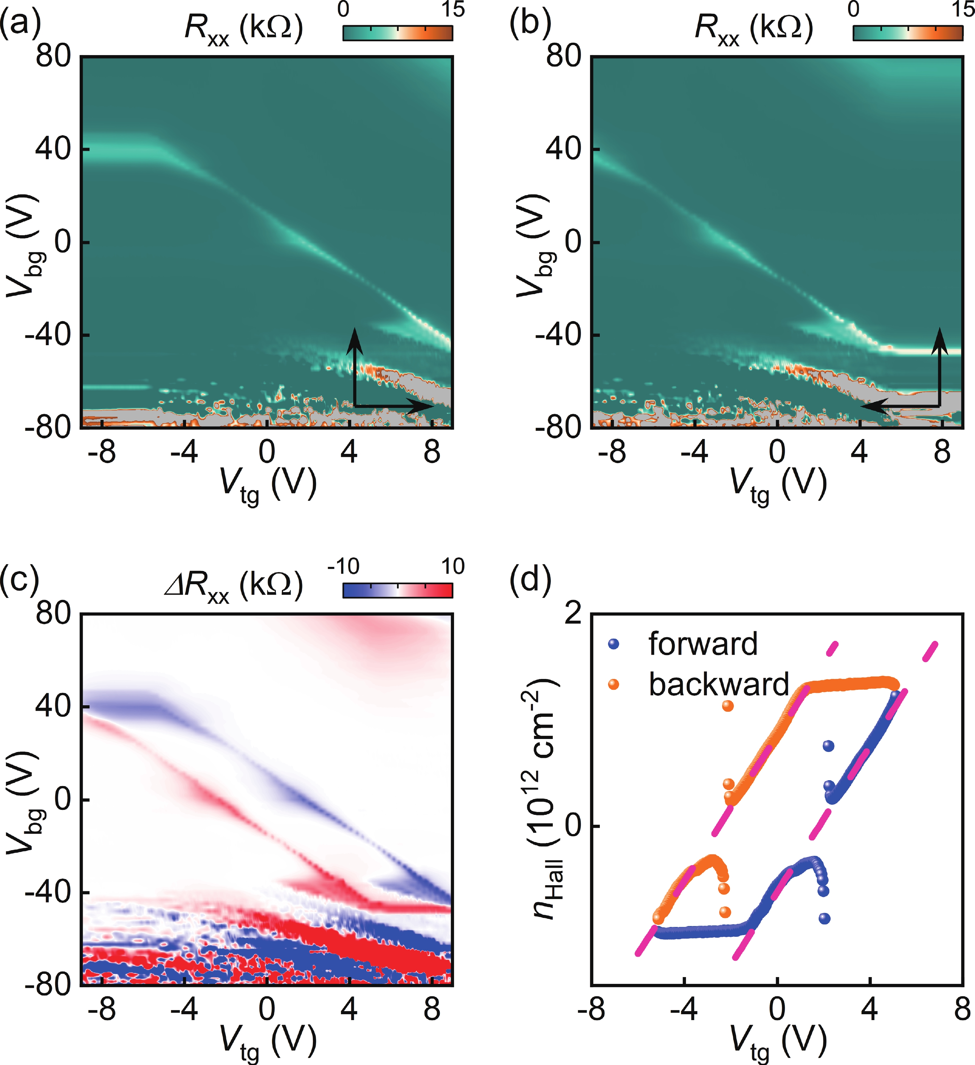
The ferroelectricity emerging in non-polar graphene/hexagonal boron nitride (hBN) heterostructures has drawn considerable attention because of its fascinating properties and promising high-frequency electrical polarization switching. Yet, the underlying mechanism is still under debate. Here in twisted double bilayer graphene (TDBLG) aligned with its neighboring hBN, we observed two types of hysteresis-delayed hysteresis in top gate induced by the anomalous screening, and advanced hysteresis in back gate caused by the anomalous gate-tunable capacitance. To investigate the role played by moiré potential in the anomalous hysteresis, we studied a moiréless graphene heterostructure. Unexpectedly, we observed exactly the same phenomena in this control device. Our findings suggest that the anomalous ferroelectricity in graphene/hBN heterostructures may originate from the dielectric material hBN, calling for further structural investigations on hBN. Further analysis indicates that those hysteresis can be asymmetric and scalable with applied external electric fields, distinct from conventional ferroelectric switching with well-defined coercive fields. The observation of gate-tunable capacitance provides more insights in the mysterious ferroelectricity in graphene/hBN heterostructures, and should enable new design of memory devices such as memcapacitor based on tunable capacitance.
Broadband gate-reconfigurable infrared sensing based on a b-As0.3P0.7/MoS2 heterojunction
Yuelin Zhang, Tangxin Li, Yuxuan Pei, Ziyue Song, Hangyu Xu, Xiao Fu, Mingkai Li, Min Luo
J. Semicond.  2026, 47(10): 102707  doi: 10.1088/1674-4926/26060028
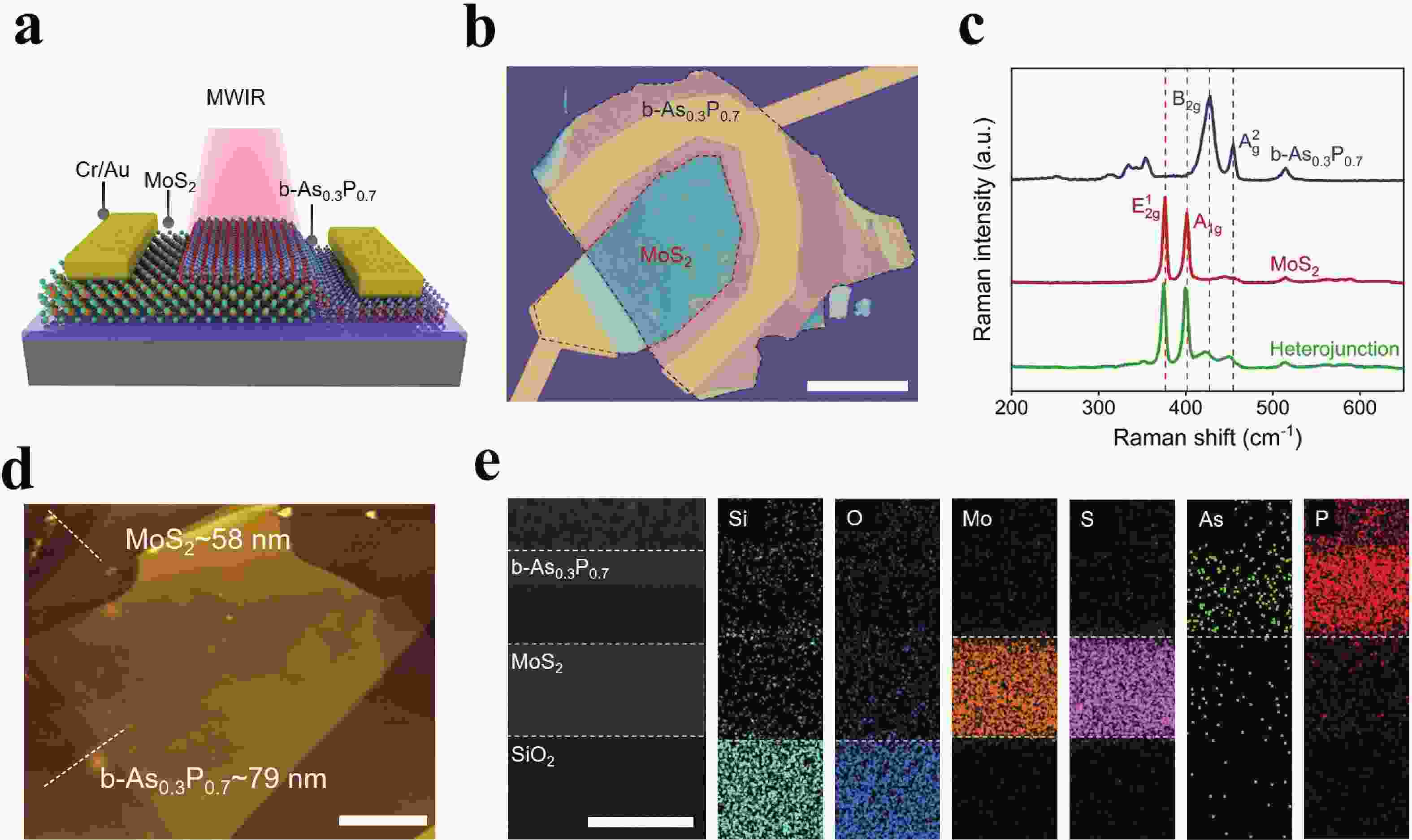
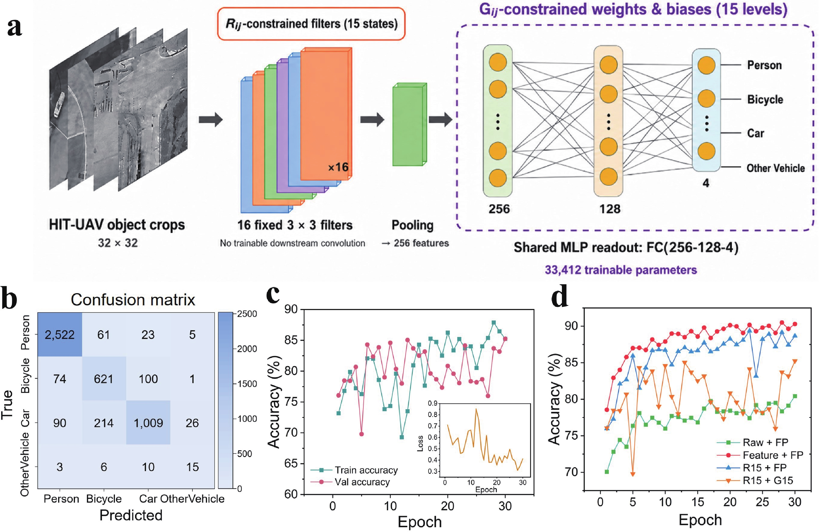
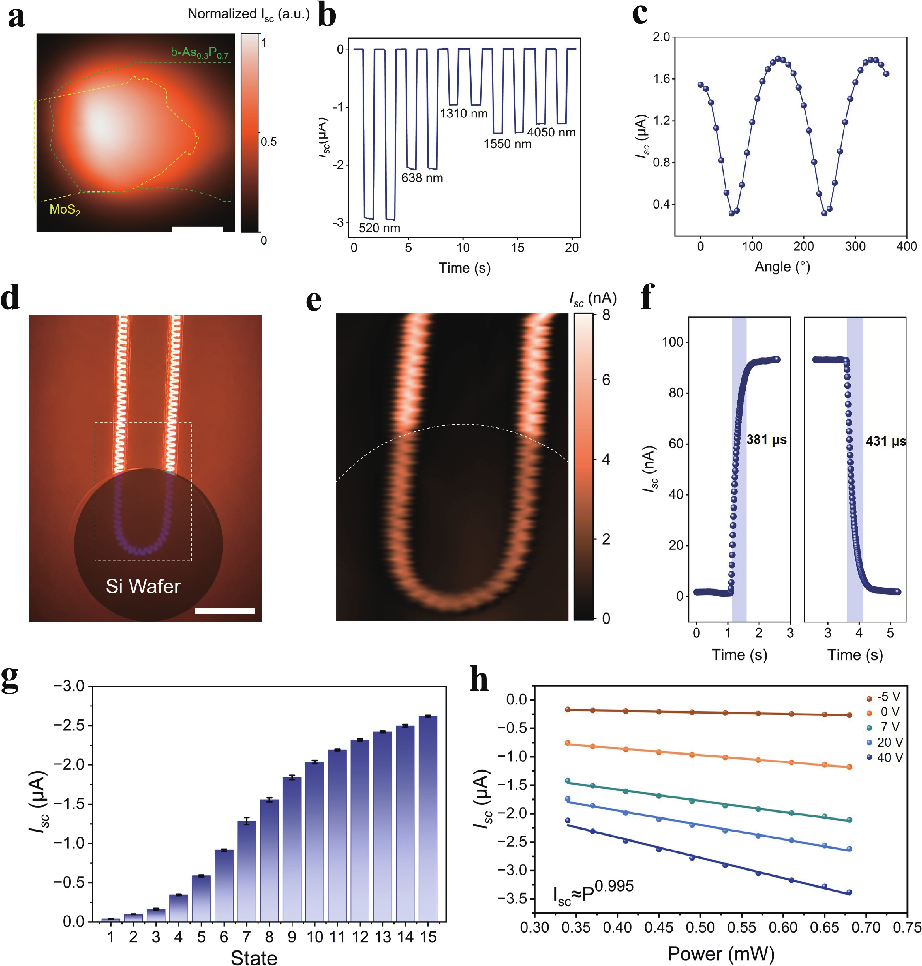
Mid-infrared light beyond 4 μm carries molecular vibrational fingerprints that are essential for gas sensing, emission monitoring and thermal-scene perception. Existing infrared systems still rely on full-frame acquisition, data conversion, transmission and back-end computation. This architecture is increasingly inefficient for distributed and mobile sensing, where power, latency and bandwidth are strictly constrained. Here we report a reconfigurable mid-infrared photodetector based on a b-As0.3P0.7/MoS2 van der Waals(vdWs) heterojunction. The narrow-bandgap b-As0.3P0.7 layer enables broadband detection from 520 nm to 4.05 μm, while the gate-tunable heterointerface reconfigures carrier separation and transport. The device produces 15 switchable photocurrent states and exhibits a response time on the order of hundreds of microseconds. We further perform hardware-aware infrared image-classification simulations, achieving a mean test accuracy of 86.75%. These results highlight the potential of reconfigurable vdW heterojunctions as programmable infrared sensing elements for future edge applications.
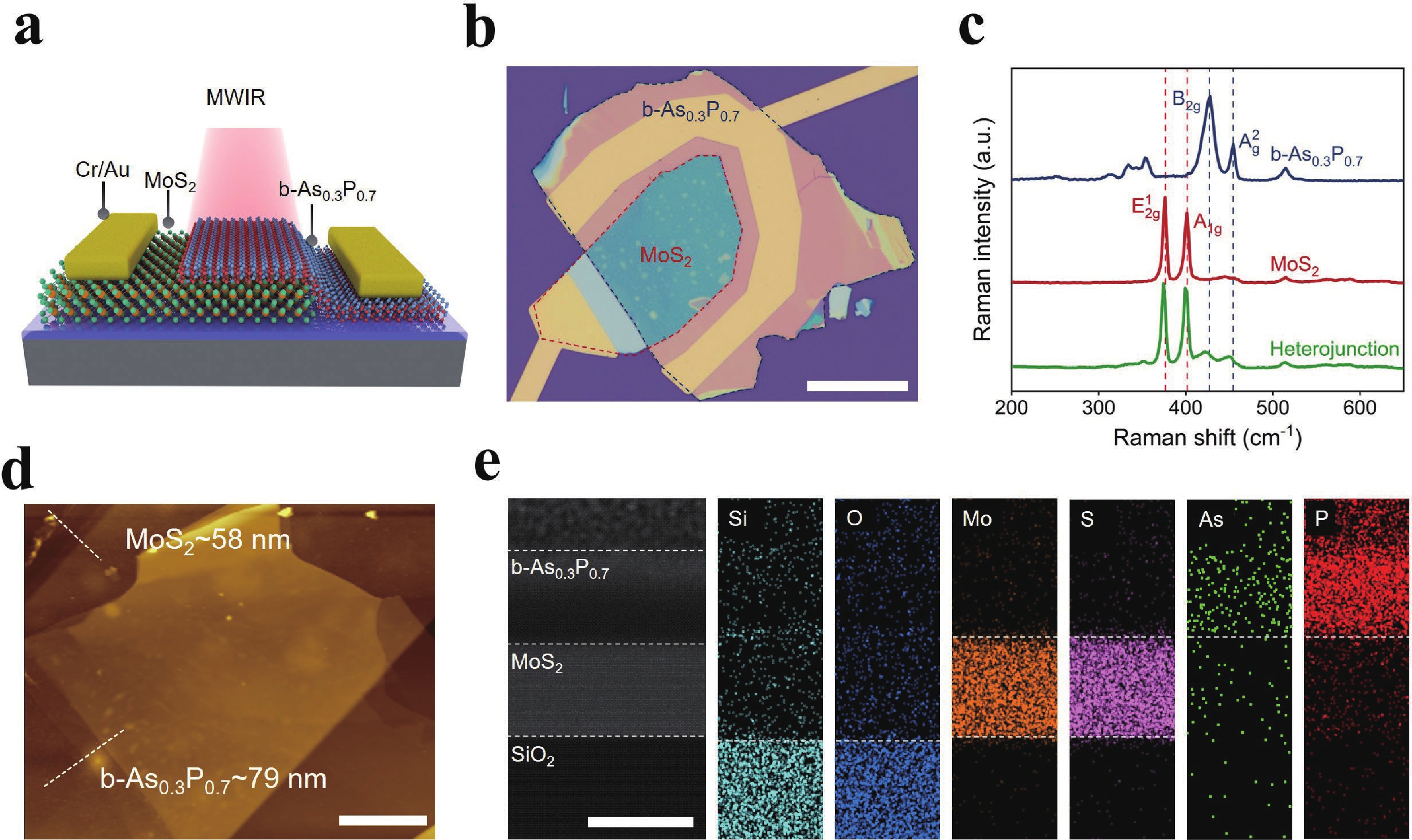
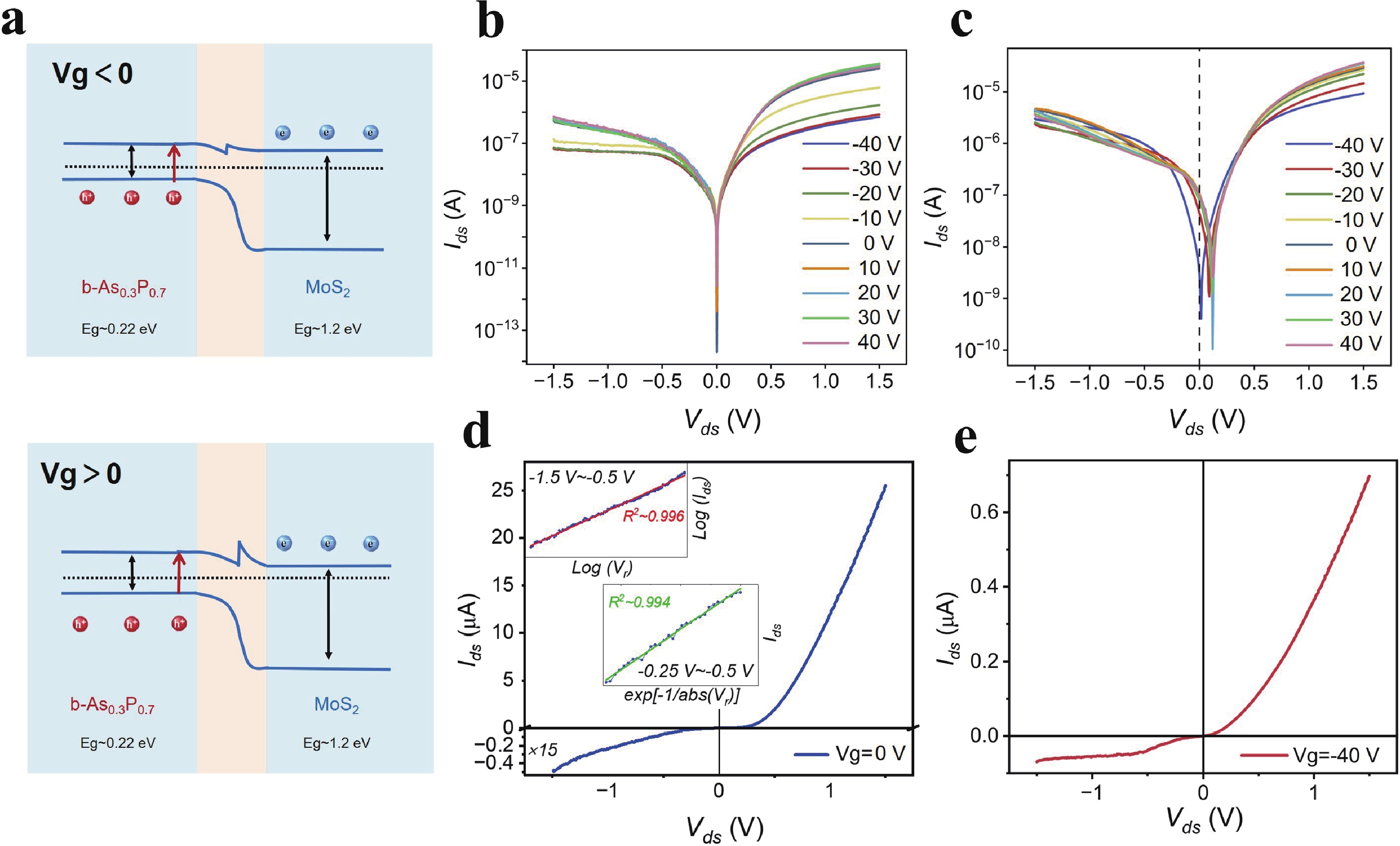
Mid-infrared light beyond 4 μm carries molecular vibrational fingerprints that are essential for gas sensing, emission monitoring and thermal-scene perception. Existing infrared systems still rely on full-frame acquisition, data conversion, transmission and back-end computation. This architecture is increasingly inefficient for distributed and mobile sensing, where power, latency and bandwidth are strictly constrained. Here we report a reconfigurable mid-infrared photodetector based on a b-As0.3P0.7/MoS2 van der Waals(vdWs) heterojunction. The narrow-bandgap b-As0.3P0.7 layer enables broadband detection from 520 nm to 4.05 μm, while the gate-tunable heterointerface reconfigures carrier separation and transport. The device produces 15 switchable photocurrent states and exhibits a response time on the order of hundreds of microseconds. We further perform hardware-aware infrared image-classification simulations, achieving a mean test accuracy of 86.75%. These results highlight the potential of reconfigurable vdW heterojunctions as programmable infrared sensing elements for future edge applications.
Controllable growth of nonlayered 2D MnS nanosheets with thickness-tunable semiconductor to metal transition
Xuejian Ma, Zunfa Wang, Chao Chen, Zongpeng Ma, Yue Tang, Hongmei Jing, Jiangbo Lu, Kaiqiang Liu, Hua Xu
J. Semicond.  2026, 47(10): 102708  doi: 10.1088/1674-4926/26080022
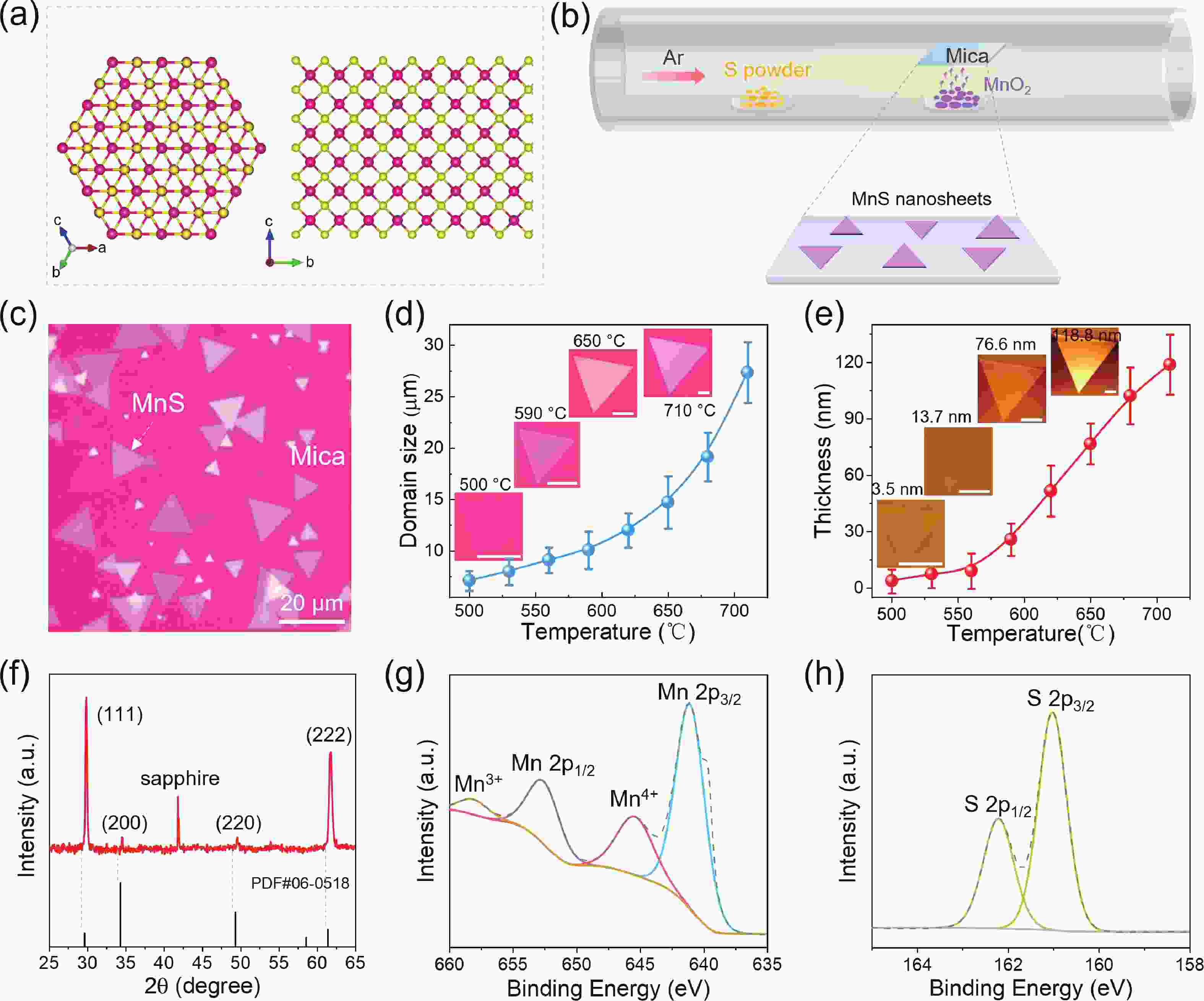
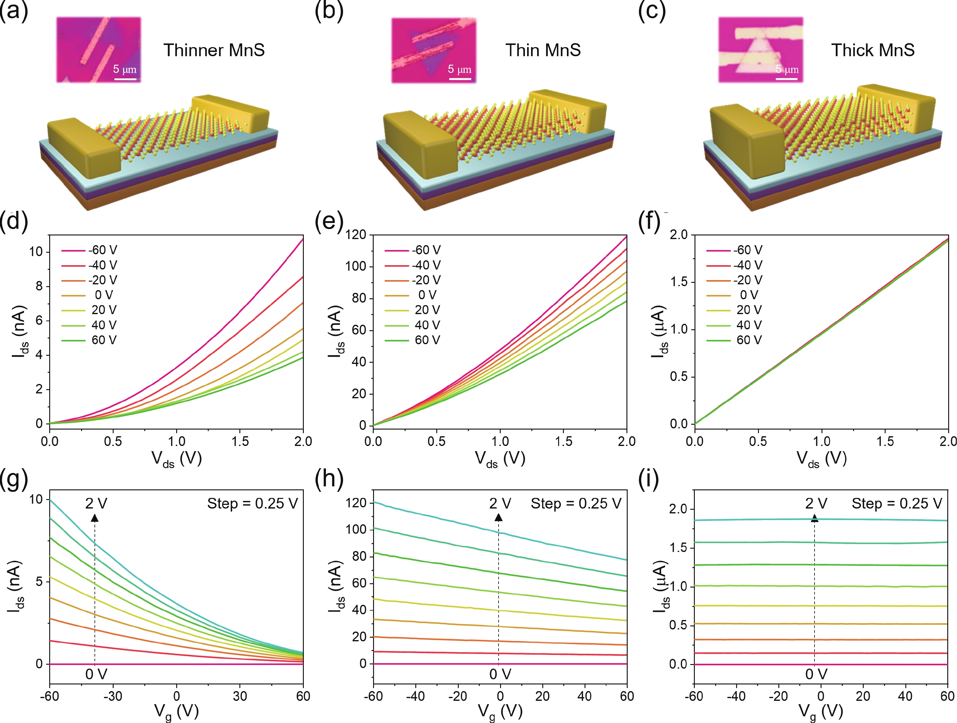
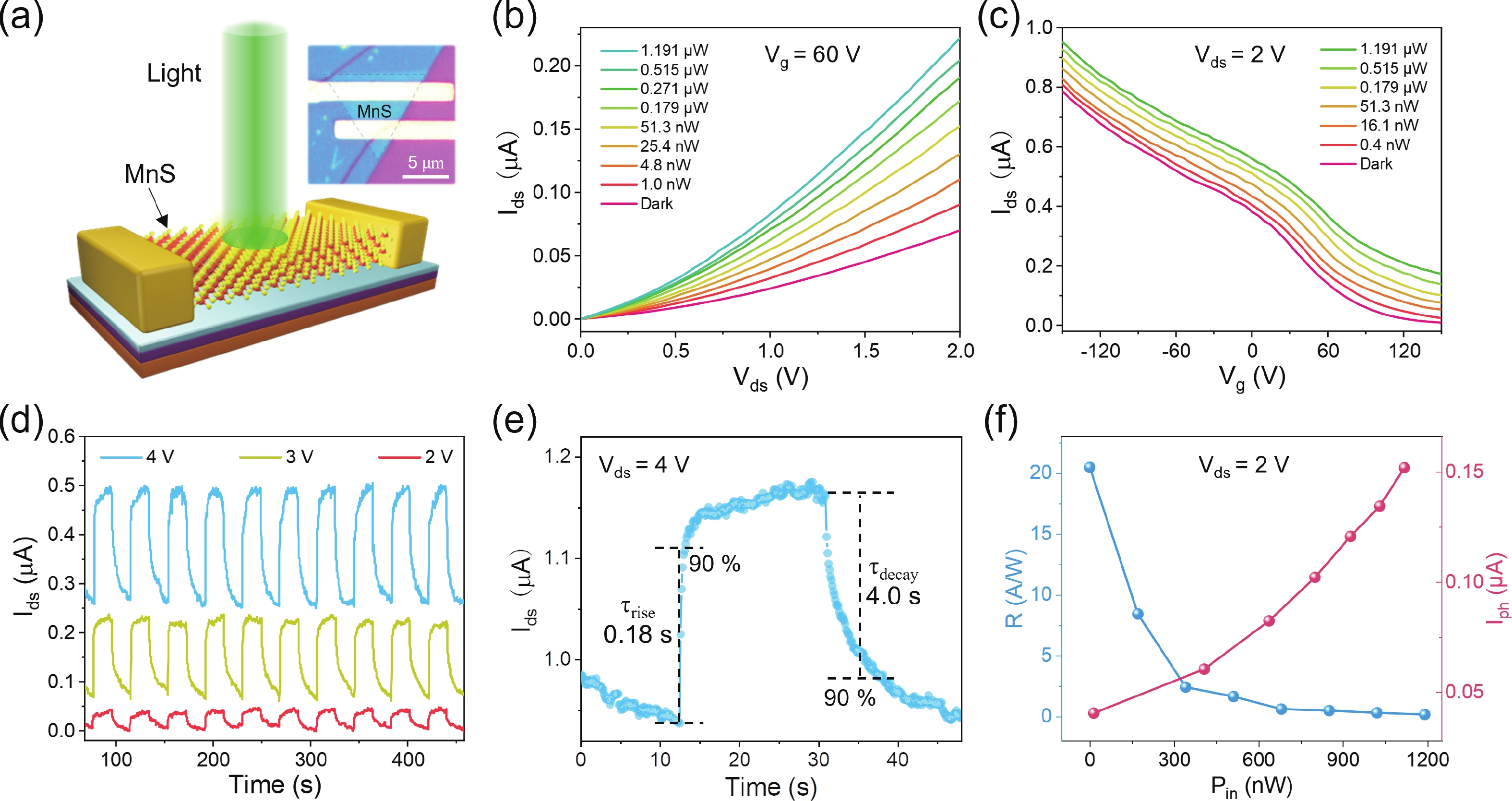
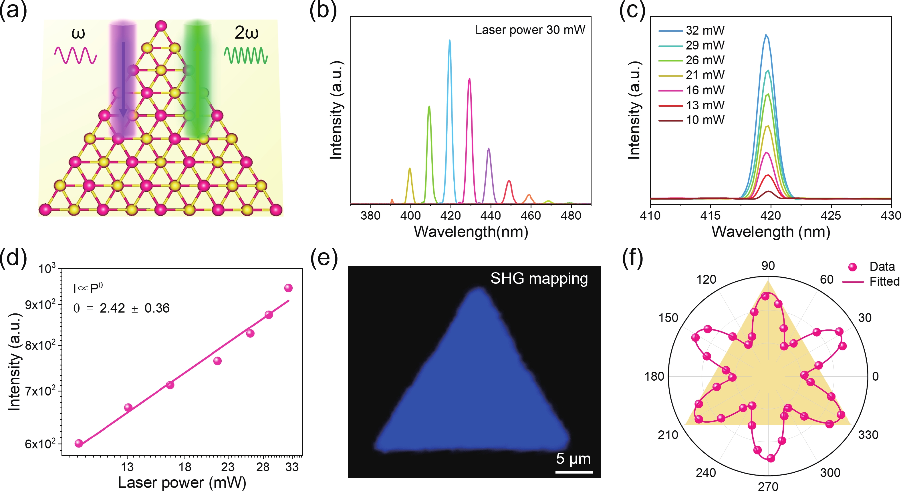
Two-dimensional (2D) materials have attracted great research interest owing to their remarkable properties and promising application in electronic and optoelectronic devices. However, modulating the electrical conduction feature of 2D materials to match the basic requirements for constructing various functional devices is still a big challenge. Herein, we report the conduction feature modulation and device application of nonlayered 2D MnS nanosheets synthesized via chemical vapor deposition (CVD). By precisely tuning the growth temperature from 500 to 710 °C, the thickness of MnS nanosheets can be continuously modulated from ~3.5 to ~118.8 nm with the grain size changing from ~5 to ~27 μm. The as-grown MnS nanosheets possess uniform triangle morphology with high crystallinity and strong second-order nonlinear optical properties. Field-effect transistors based on MnS nanosheets exhibit an interesting conduction feature transition from p-type semiconductor to metal as the thickness increasing from thinner to thick. As results, the photodetector based on thinner MnS semiconductor achieves superior photoresponsivity of 20.47 A/W, high detectivity of 5.31 × 10¹⁰ Jones, and relative fast response time of 180 ms. Our findings not only enrich the family of intrinsic p-type 2D materials but also open a new avenue for electrical property engineering in non-layered 2D materials.
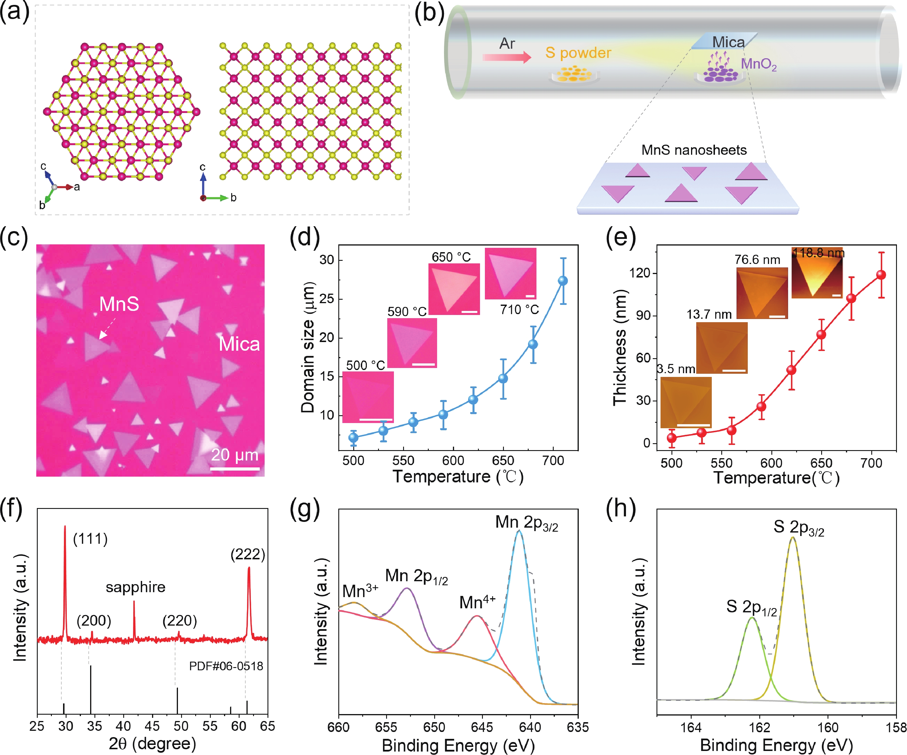
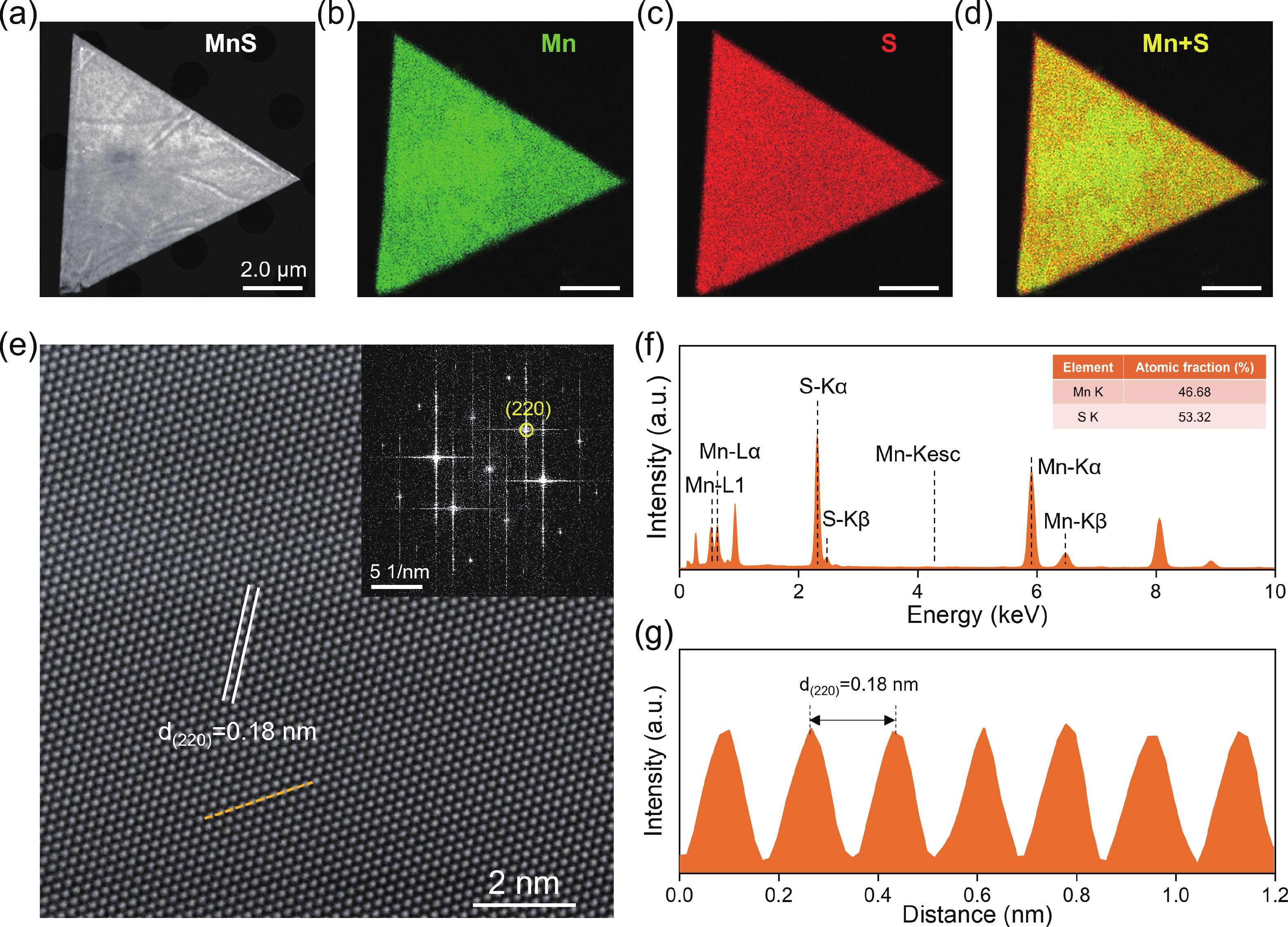
Two-dimensional (2D) materials have attracted great research interest owing to their remarkable properties and promising application in electronic and optoelectronic devices. However, modulating the electrical conduction feature of 2D materials to match the basic requirements for constructing various functional devices is still a big challenge. Herein, we report the conduction feature modulation and device application of nonlayered 2D MnS nanosheets synthesized via chemical vapor deposition (CVD). By precisely tuning the growth temperature from 500 to 710 °C, the thickness of MnS nanosheets can be continuously modulated from ~3.5 to ~118.8 nm with the grain size changing from ~5 to ~27 μm. The as-grown MnS nanosheets possess uniform triangle morphology with high crystallinity and strong second-order nonlinear optical properties. Field-effect transistors based on MnS nanosheets exhibit an interesting conduction feature transition from p-type semiconductor to metal as the thickness increasing from thinner to thick. As results, the photodetector based on thinner MnS semiconductor achieves superior photoresponsivity of 20.47 A/W, high detectivity of 5.31 × 10¹⁰ Jones, and relative fast response time of 180 ms. Our findings not only enrich the family of intrinsic p-type 2D materials but also open a new avenue for electrical property engineering in non-layered 2D materials.
A photolithography-compatible method for transferring full-device constituents on silicon substrate
Zunxian Lv, Shun Zhang, Mingjian Yang, Xinsheng Wang, Zhaochao Liu, Yameng Hou, Jiabiao Chen, Moyuan Cao, Feng Luo, Jinxiong Wu
J. Semicond.  2026, 47(10): 102709  doi: 10.1088/1674-4926/26080030
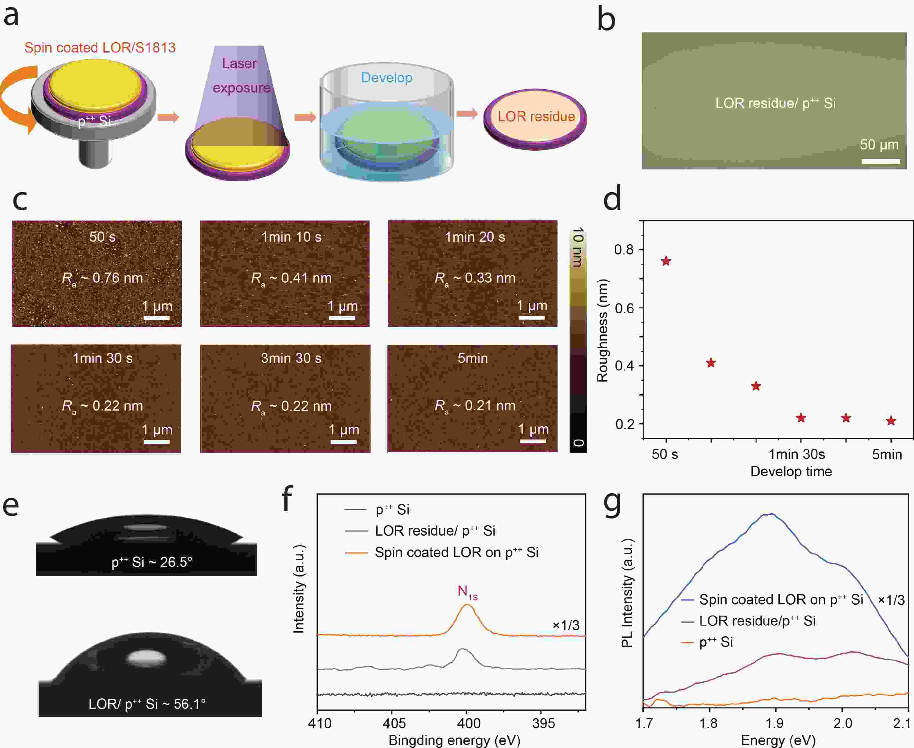
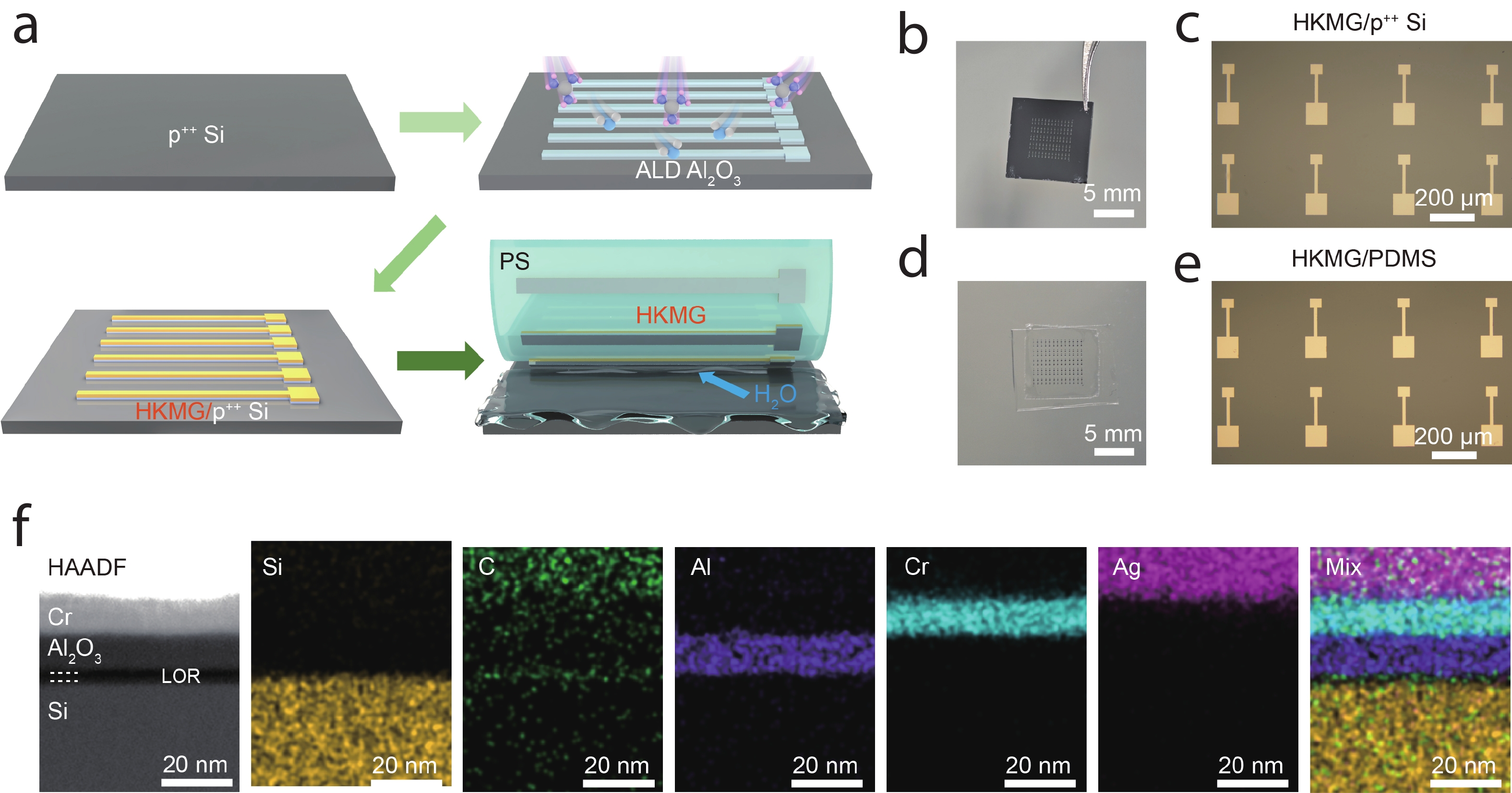
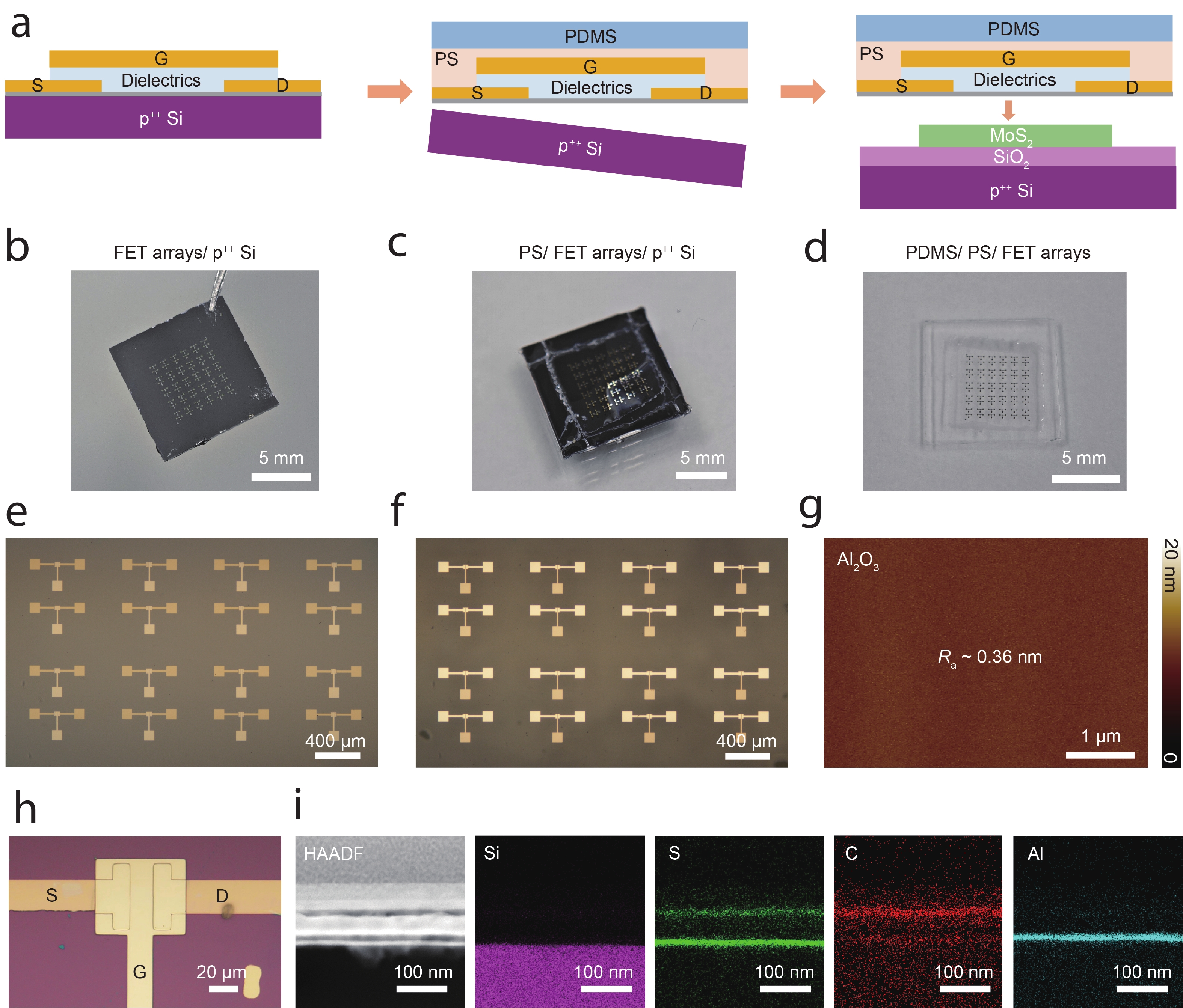
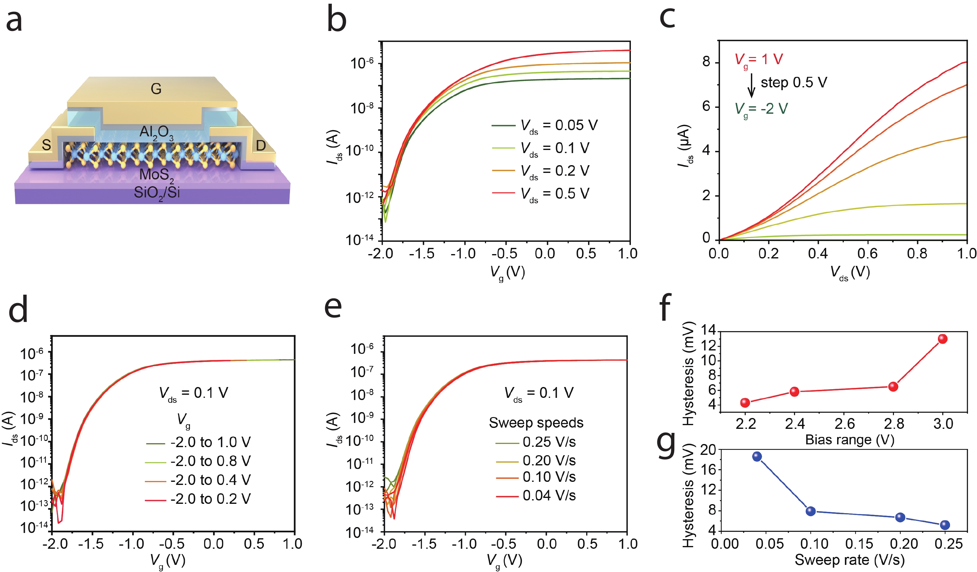
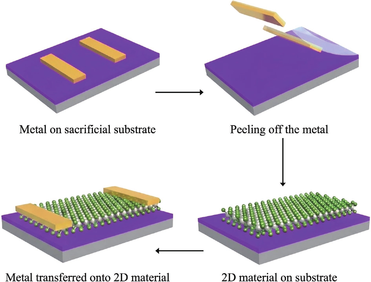
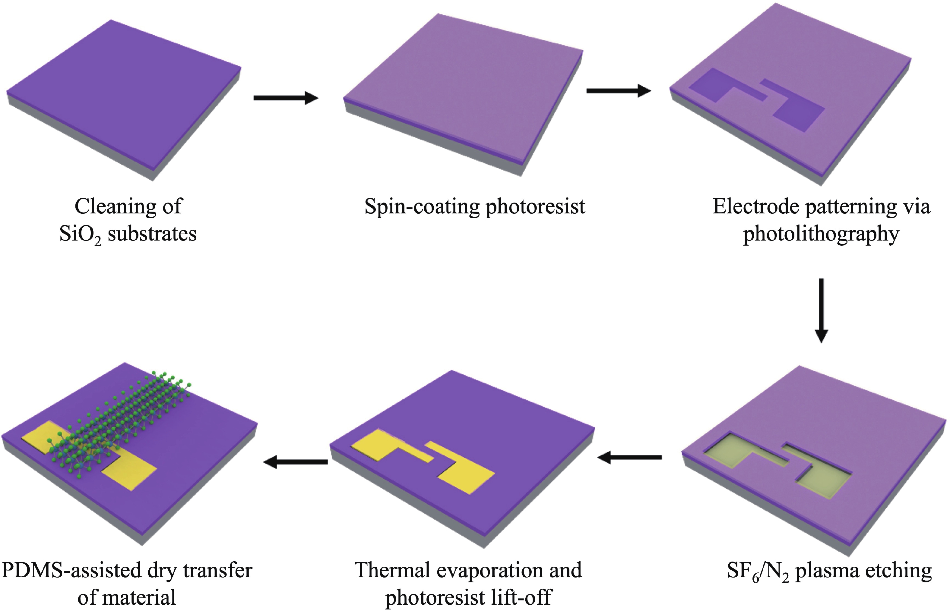
Transfer printing offers a promising route to integrate pre-fabricated device components with two-dimensional (2D) semiconductors, yet most existing approaches rely on deliberately deposited buffer layers or specialized substrates, adding complexity and limiting compatibility with standard silicon fabrication. Here, we report a simple and photolithography-compatible strategy that leverages the ultrathin lift-off-resist (LOR) residue, which naturally retains on a commercial silicon substrate after standard photolithography, as a sacrificial release layer. This ~2 nm-thick residue allows selective water intercalation at the LOR/Si interface, enabling damage-free delamination of various pre-fabricated metal electrodes, high-κ metal gate (HKMG) stacks, and even entire device stacks directly from the Si substrate. Besides, the top-gated MoS2 transistor was fabricated by one-step laminating the full-device stack onto the MoS2 flake, yielding a clean van der Waals interface, small subthreshold swing and negligible gate hysteresis. Our method eliminates the need for additional sacrificial layer deposition or specialized handling substrates, offering a facile method to transfer full-device constituents on industry-compatible Si substrate.
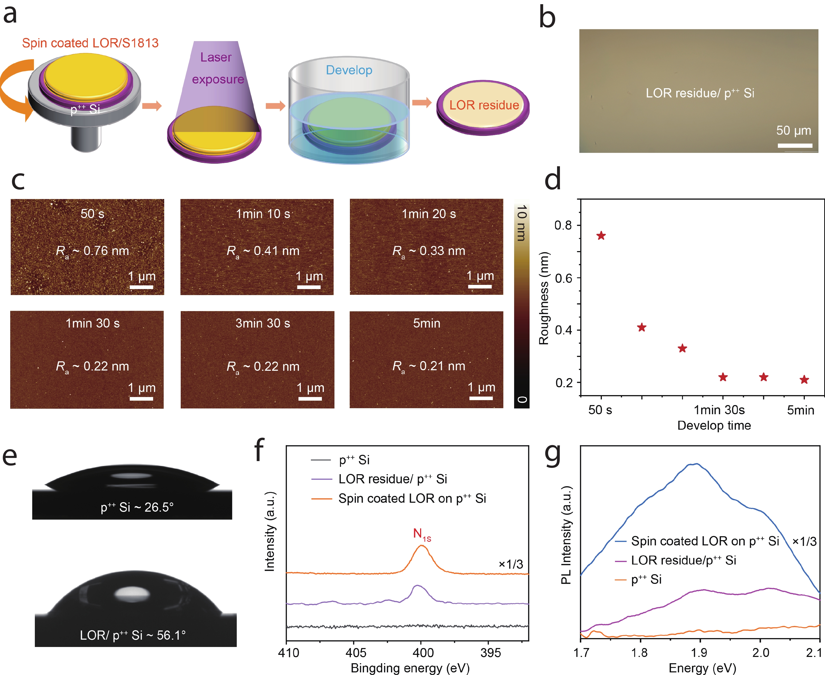
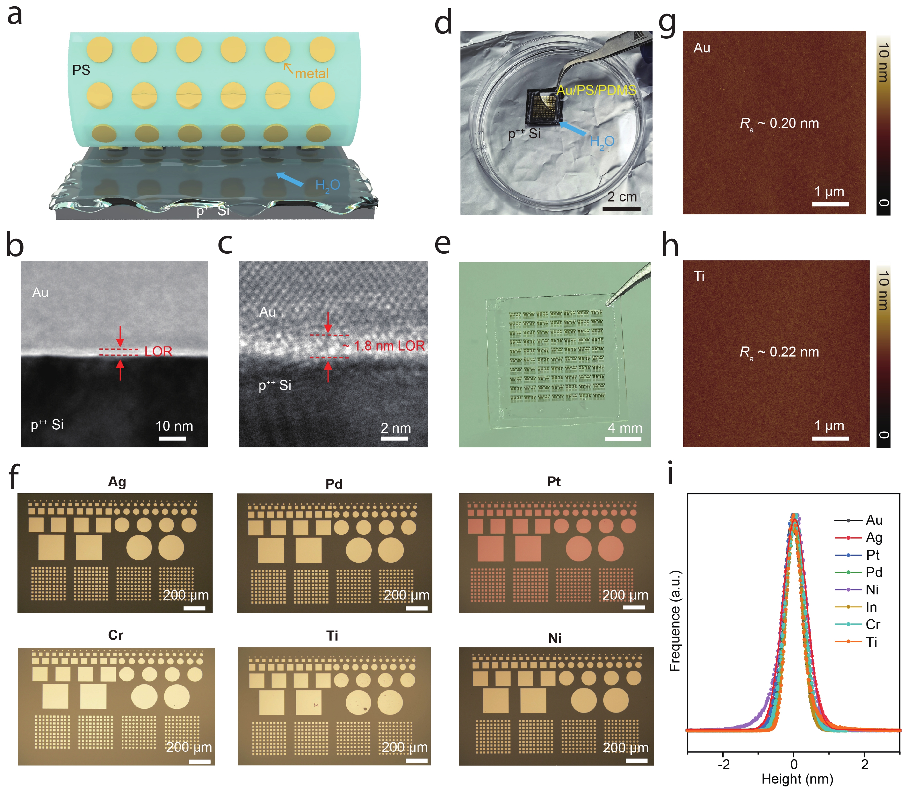
Transfer printing offers a promising route to integrate pre-fabricated device components with two-dimensional (2D) semiconductors, yet most existing approaches rely on deliberately deposited buffer layers or specialized substrates, adding complexity and limiting compatibility with standard silicon fabrication. Here, we report a simple and photolithography-compatible strategy that leverages the ultrathin lift-off-resist (LOR) residue, which naturally retains on a commercial silicon substrate after standard photolithography, as a sacrificial release layer. This ~2 nm-thick residue allows selective water intercalation at the LOR/Si interface, enabling damage-free delamination of various pre-fabricated metal electrodes, high-κ metal gate (HKMG) stacks, and even entire device stacks directly from the Si substrate. Besides, the top-gated MoS2 transistor was fabricated by one-step laminating the full-device stack onto the MoS2 flake, yielding a clean van der Waals interface, small subthreshold swing and negligible gate hysteresis. Our method eliminates the need for additional sacrificial layer deposition or specialized handling substrates, offering a facile method to transfer full-device constituents on industry-compatible Si substrate.