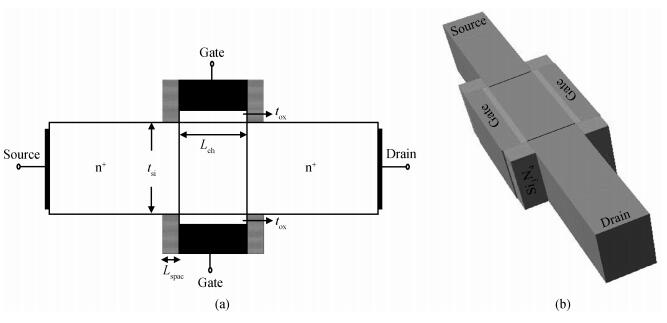
Abstract: This article presents the bias and geometry optimization procedure for the radio frequency (RF) stability performance of nanoscale symmetric double-gate metal-oxide semiconductor field-effect transistors (DG-MOSFETs). The stability model can provide hints for optimizing the DG-MOSFET under an RF range. The device parameters are extracted for different bias and geometry conditions through numerical simulation, and the RF figures of merit such as cut-off frequency (ft) and maximum oscillation frequency (fmax), along with stability factor, are calculated for an optimized structure. The proposed structure exhibits good RF stability performance.
The scaling of conventional planar MOSFETs down to the sub-50 nm regime leads to an increase in leakage currents and short channel effects (SCEs), which causes severe problems in the switching operations. In order to obtain an improved performance, double-gate MOSFETs were proposed for better SCE suppression capability, higher current drive capability, lower leakage current and better scaling capability[1, 2]. In recent years, DG-MOSFETs have become popular for analog and RF applications due to the volume inversion effect at low gate bias. The impact of structural parameter fluctuation on the RF performance of DG-MOSFETs was studied and the optimized structure reported[3]. The impact of gate and channel engineering on the RF performance of DG-MOSFETs was also studied[4] and shows that a dual material (DM) work function for the gate has better RF performance as compared to halo-doped channel DG-MOSFETs. Recently, graded channel (GC) technology, gate stack engineering (GS), the DM work function gate and combinations of these technologies, i.e., GCGSDG and GSDMDG, were studied for analog and RF performance[5]. The optimized DG-MOSFET design using DM and GC requires additional effort in processing steps such as the metal wet etch process, metal inter diffusion process, and selective implantation to maintain the dual work function in DM devices. Selective tilted ion implantation is required for GC devices. However, studies on the stability performance of DG-MOSFETs have not received attention, and this is one of the most important parameters for radio frequency integrated circuit (RFIC) design.
In our previous work, we studied the RF stability of silicon nanowire transistors[6] and this article presents the stability performance of optimized DG-MOSFETs in the RF range. We have discussed the bias and geometry optimization procedure of DG-MOSFET in detail.
2.
Device structure and simulation
Figure 1(a) shows the cross sectional view and Figure 1(b) shows the 3D schematic structure of a symmetric DG-MOSFET with a physical channel length (Lch) of 22 nm and gate oxide thickness (tox) of 1.6 nm, as per ITRS[7]. The DG-MOSFET has an n+ source and drain with a doping concentration of 2 × 1020 cm−3 and channel doping of 1015 cm−3. Si3N4 is used as the gate spacer material to provide mechanical strength to the gate. HfO2 is used as the gate dielectric, which reduces gate tunneling leakage current, and the gate electrode work function is considered as 4.15 eV. Electric field dependent carrier mobility with velocity saturation, band gap narrowing, a Lombardi constant voltage and temperature (CVT), along with a concentration-dependent mobility model, were activated for simulation. Fermi-Dirac statistics, Shockley Read Hall and auger recombination for minority carrier recombination have been used, along with a density gradient quantum correction model, for inversion layer quantum effects for simulation[8]. The AC characteristics were performed to extract two port Y and Z parameters. The extracted parasitic resistances and capacitances from device simulation are used to calculate the RF FoM of the DG-MOSFET. The device simulations were performed using a Silvaco ATLAS device simulator.
Figure
1.
(a) Cross-section view and (b) 3-D schematic view of a symmetric DG-MOSFET
The stability factor, K, gives an indication as to whether a device is conditionally or unconditionally stable. The DG-MOSFET is unconditionally stable at any operating frequency above a critical frequency (fk). Unconditionally stable means that the transistor will not begin to oscillate independently from the value of the signal source and load impedances from any additional passive termination networks at the transistor's input and output[9]. At an operating frequency below fk, however, the transistor is conditionally stable and certain termination conditions can cause oscillation. Hence, the device must satisfy the condition K> 1 to be unconditionally stable[10]. The stability factor is calculated using Y-parameters at different frequencies of operation for the DG-MOSFET. The stability factor in terms of Y-parameter can be expressed as[11]
K=2Re(Y11)Re(Y22)−Re(Y12Y21)|Y12Y21|.
(1)
This article focuses on a symmetric DG-MOSFET which has three terminals. Both the gates are tied to form a single gate terminal, and there are source and drain terminals. The Y-parameters are considered with intrinsic small signal parameters of symmetric DG-MOSFETs as[12]
Y11≈ω2RgdC2gd+jω(Cgs+Cgd),
(2)
Y12≈−ω2RgdC2gd+jωCgd,
(3)
Y21≈−ω2RgdC2gd−jω(Cgd+τgm),
(4)
Y22≈gds+ω2RgdC2gd+jωCgd.
(5)
These Y parameters can be used in Eq. (1) to simplify further as
where Cgs is the total gate-to-source, Cgd is the total gate-to-drain and Cgg is the total gate capacitance (Cgg=Cgs+Cgd), gm is the transconductance, gds is the drain to source conductance, Rgs is the gate-to-source resistance and Rgd is the gate-to-drain resistance.
Equation (6) is extended to obtain fk by substituting K= 1 and by making approximation ω4R2gdC4gd≪ 1, ω4R2gsC4gs≪ 1, and ω2τ2m≪ 1.
fk≅ftN√gdsgmRgsM2+NM(gmRgd+1),
(7)
where M=CgsCgg, N=CgdCgg, and ft=gm2πCgg.
The total Cgs and Cgd without considering overlap capacitance and external fringing capacitance can be calculated as[13]
where εSi and εox are the dielectric constants of silicon and oxide; W, tsi, and tox are the width and thickness of the silicon body and the gate oxide thickness, respectively. VFB and ϕf are the flat band voltage and Fermi potential, respectively. Equation (7) describes the relation between fk, the intrinsic small signal parameters and ft, which also provides a hint for the optimization. It is clear from Eq. (7) that the M and N values can be adjusted to reduce fk without ft degradation. But N is almost an independent parameter on the stability model with respect to ft. The optimization begins with the study of factors related to M and N, especially Cgs, Cgd and Cgg. Equations (8)-(10) show the bias and geometry dependence on Cgs and Cgd of the DG-MOSFET. By adjusting the applied gate and drain bias, and the geometrical parameters such as tsi and spacer length (Lspac), the DG-MOSFET can be optimized for better stability performance.
4.
Results and discussion
The stability factor is calculated from the extracted Y-parameters for various applied gate (Vgs) biases with a drain (Vds) bias of 0.8 V, and is shown in Fig. 2. It is evident from Fig. 2 that the DG-MOSFET attains an unconditionally stable condition at higher Vgs since Cgs dominates Cgd at higher gate bias.
Figure
2.
The extracted stability factor for different Vgs at Vds = 0.8 V
Figure 3 shows the extracted stability factor for various Vds at Vgs = 1.2 V. As Vds increases, the stability performance degrades due to degradation in Cgd, and drain induced barrier lowering (DIBL) also affects device performance at higher Vds. Hence, a smaller drain bias is preferred to operate the DG-MOSFET in the RF range.
Figure
3.
The extracted stability factor for different Vds at Vgs = 1.2 V
Figure 4 shows the critical frequency (fk) as a function of gate voltage (Vgs). The fk reduces with the increase in gate bias and further reduces with a smaller applied Vds. This shows that at smaller drain biases and higher gate biases, the DG-MOSFET exhibits better RF stability performance.
Figure
4.
Critical frequency as a function of gate voltage
Figure 5 shows the extracted stability factor and Cgd for various silicon body thicknesses (tsi). It is evident that for thinner tsi, stability is reached at an earlier frequency compared to thicker tsi, since Cgd decreases with thinner tsi. However, tsi cannot be reduced further as it leads to an increase in device oscillation at higher frequency. The parasitic source and drain resistance increases with thinner tsi, which also increases the SCEs. The optimized tsi for better RF stability is 10 nm, comparable to the ITRS requirement[6] for ultra-thin silicon body thickness.
Figure
5.
The extracted stability factor and Cgd for different silicon body thicknesses
Figure 6 shows the extracted stability factor and Cgd for different spacer lengths (Lspac). Lspac has an impact on the RF stability performance of DG-MOSFETs. The fringing capacitance increases with thinner Lspac, thereby causing oscillation at higher frequency. The DG-MOSFET becomes stable at fk = 4 GHz for an Lspac of 20 nm as Cgd decreases with Lspac. A further increase in Lspac will not have any impact on stability because Cgd is saturated for larger Lspac.
Figure
6.
The extracted stability factor and Cgd for different spacer lengths
The DG-MOSFET exhibits better stability performance at tsi = 10 nm, tox = 1.6 nm and Lspac = 20 nm. Figure 7 shows the extracted stability factor for the optimized structure. It is evident that K reaches 1 at 7.5 GHz which shows that the device can be operated as unconditionally stable from 7.5 GHz onwards. This indicates that the DG-MOSFET does not require an additional circuit when operated from 7.5 GHz onwards in RFICs.
Figure
7.
The extracted stability factor for the optimized DG-MOSFET at Vgs = 1.2 V and Vds = 0.8 V
It is necessary to observe ft and fmax to understand the capability of the DG-MOSFET under the RF range. The cut-off frequency ft is evaluated as the frequency for which the magnitude of the short circuit gain drops to unity, which can be expressed as ft=gm/2πCgg. The fmax is related to the capability of the device to provide power gain at large frequencies, and is defined as the frequency at which the magnitude of the maximum available power gain drops to unity. It is given by fmax=ft/√4(Rs+Rg+Ri)(Rds+2πftCgd), where gds is the drain to source conductance and Rg, Rs and Ri are the gate, source and channel resistances, respectively. The gate resistance is obtained from the extrinsic parasitic model, which can be expressed as Re(Z12) = Re(Z21) = Rg.
Figure 8 shows the variation in ft and fmax with drain current for the optimized DG-MOSFET. The bias and geometry optimized structure has an ft of 650 GHz due to the improved gm and fmax of 700 GHz, which shows that the proposed DG-MOSFET structure is suitable for high-speed switching and high-frequency applications.
Figure
8.
The variation of ft and fmax with drain current for the optimized DG-MOSFET at Vgs = 1.2 V and Vds = 0.8 V
The RF stability model is developed for a DG-MOSFET, and its stability characteristics are performed through TCAD simulation. The stability of the device is studied for various bias and geometry conditions, and it is observed that Cgd and Cgs are responsible for the degradation in fk. The proposed optimized geometry and bias conditions show excellent stability performance. No additional circuit is required as the device is unconditionally stable from 7.5 GHz onwards.
Sorin C, Gacuteéard G, Thierry O, et al. Ultimately thin double-gate SOI MOSFETs. IEEE Trans Electron Devices, 2003, 50(3):830 doi: 10.1109/TED.2003.811371
[3]
Liang J, Xiao H, Huang R, et al. Design optimization of structural parameters in double gate MOSFETs for RF application. Semicond Sci Technol, 2008, 23(5):1 doi: 10.1007%2F978-3-642-19542-6_93.pdf
[4]
Mohankumar N, Syamal B, Sarkar C K. Influence of channel and gate engineering on the analog and RF performance of DG MOSFETs. IEEE Trans Electron Devices, 2010, 57(4):820 doi: 10.1109/TED.2010.2040662
[5]
Sharma R K, Gupta M, Gupta R S. TCAD assessment of device design technologies for enhanced performance of nanoscale DG MOSFET. IEEE Trans Electron Devices, 2011, 58(9):2936 doi: 10.1109/TED.2011.2160065
[6]
Sivasankaran K, Kannadassan D, Seetaram K, et al. Bias and geometry optimization of silicon nanowire transistor:radio frequency stability perspective. Microw Opt Technol Lett, 2012, 54(9):2114 doi: 10.1002/mop.27016
[7]
International Technology Roadmaps for Semiconductor (ITRS), 2005
[8]
Device simulator ATLAS user manual. Silvaco Int. , Santa Clara, CA, May 2006[Online Available]: http://silvaco.com
[9]
Schwierz F, Liou J J. Semiconductor devices for RF applications:evolution and current status. Microelectron Reliab, 2001, 41:145 doi: 10.1016/S0026-2714(00)00076-7
[10]
Gonzales G. Microwave transistor amplifiers——analysis and design. 2nd ed. Prentice-Hall, 1997
[11]
Rollet J M. Stability and power gain invariants of linear two ports. IRE Trans Circuit Theory, 1962, 9:29 doi: 10.1109/TCT.1962.1086854
[12]
Cho S, Kim K R, Park B G, et al. RF performance and small-signal parameter extraction of junctionless silicon nanowire MOSFETs. IEEE Trans Electron Devices, 2011, 58(5):1388 doi: 10.1109/TED.2011.2109724
[13]
Sarkar A, Das A K, De S, et al. Effect of gate engineering in double-gate MOSFETs for analog/RF applications. Microelectron J, 2012, 43(11):873 doi: 10.1016/j.mejo.2012.06.002
Fig. 1.
(a) Cross-section view and (b) 3-D schematic view of a symmetric DG-MOSFET
Sorin C, Gacuteéard G, Thierry O, et al. Ultimately thin double-gate SOI MOSFETs. IEEE Trans Electron Devices, 2003, 50(3):830 doi: 10.1109/TED.2003.811371
[3]
Liang J, Xiao H, Huang R, et al. Design optimization of structural parameters in double gate MOSFETs for RF application. Semicond Sci Technol, 2008, 23(5):1 doi: 10.1007%2F978-3-642-19542-6_93.pdf
[4]
Mohankumar N, Syamal B, Sarkar C K. Influence of channel and gate engineering on the analog and RF performance of DG MOSFETs. IEEE Trans Electron Devices, 2010, 57(4):820 doi: 10.1109/TED.2010.2040662
[5]
Sharma R K, Gupta M, Gupta R S. TCAD assessment of device design technologies for enhanced performance of nanoscale DG MOSFET. IEEE Trans Electron Devices, 2011, 58(9):2936 doi: 10.1109/TED.2011.2160065
[6]
Sivasankaran K, Kannadassan D, Seetaram K, et al. Bias and geometry optimization of silicon nanowire transistor:radio frequency stability perspective. Microw Opt Technol Lett, 2012, 54(9):2114 doi: 10.1002/mop.27016
[7]
International Technology Roadmaps for Semiconductor (ITRS), 2005
[8]
Device simulator ATLAS user manual. Silvaco Int. , Santa Clara, CA, May 2006[Online Available]: http://silvaco.com
[9]
Schwierz F, Liou J J. Semiconductor devices for RF applications:evolution and current status. Microelectron Reliab, 2001, 41:145 doi: 10.1016/S0026-2714(00)00076-7
[10]
Gonzales G. Microwave transistor amplifiers——analysis and design. 2nd ed. Prentice-Hall, 1997
[11]
Rollet J M. Stability and power gain invariants of linear two ports. IRE Trans Circuit Theory, 1962, 9:29 doi: 10.1109/TCT.1962.1086854
[12]
Cho S, Kim K R, Park B G, et al. RF performance and small-signal parameter extraction of junctionless silicon nanowire MOSFETs. IEEE Trans Electron Devices, 2011, 58(5):1388 doi: 10.1109/TED.2011.2109724
[13]
Sarkar A, Das A K, De S, et al. Effect of gate engineering in double-gate MOSFETs for analog/RF applications. Microelectron J, 2012, 43(11):873 doi: 10.1016/j.mejo.2012.06.002
Sui Xiaohong, Liu Jinbin, Gu Ming, Pei Weihua, Chen Hongda, et al.
Chinese Journal of Semiconductors , 2005, 26(12): 2275-2280.
Search
GET CITATION
K Sivasankaran, P S Mallick. Stability performance of optimized symmetric DG-MOSFET[J]. Journal of Semiconductors, 2013, 34(10): 104001. doi: 10.1088/1674-4926/34/10/104001
K Sivasankaran, P S Mallick. Stability performance of optimized symmetric DG-MOSFET[J]. J. Semicond., 2013, 34(10): 104001. doi: 10.1088/1674-4926/34/10/104001.
Export: BibTexEndNote
Share:
Article Metrics
Article views: 2724 TimesPDF downloads: 33 TimesCited by: 0 Times
History
Received: 14 March 2013Revised: 22 April 2013Online:Published: 01 October 2013
K Sivasankaran, P S Mallick. Stability performance of optimized symmetric DG-MOSFET[J]. Journal of Semiconductors, 2013, 34(10): 104001. doi: 10.1088/1674-4926/34/10/104001 ****K Sivasankaran, P S Mallick. Stability performance of optimized symmetric DG-MOSFET[J]. J. Semicond., 2013, 34(10): 104001. doi: 10.1088/1674-4926/34/10/104001.
Citation:
K Sivasankaran, P S Mallick. Stability performance of optimized symmetric DG-MOSFET[J]. Journal of Semiconductors, 2013, 34(10): 104001. doi: 10.1088/1674-4926/34/10/104001
****
K Sivasankaran, P S Mallick. Stability performance of optimized symmetric DG-MOSFET[J]. J. Semicond., 2013, 34(10): 104001. doi: 10.1088/1674-4926/34/10/104001.
This article presents the bias and geometry optimization procedure for the radio frequency (RF) stability performance of nanoscale symmetric double-gate metal-oxide semiconductor field-effect transistors (DG-MOSFETs). The stability model can provide hints for optimizing the DG-MOSFET under an RF range. The device parameters are extracted for different bias and geometry conditions through numerical simulation, and the RF figures of merit such as cut-off frequency (ft) and maximum oscillation frequency (fmax), along with stability factor, are calculated for an optimized structure. The proposed structure exhibits good RF stability performance.
The scaling of conventional planar MOSFETs down to the sub-50 nm regime leads to an increase in leakage currents and short channel effects (SCEs), which causes severe problems in the switching operations. In order to obtain an improved performance, double-gate MOSFETs were proposed for better SCE suppression capability, higher current drive capability, lower leakage current and better scaling capability[1, 2]. In recent years, DG-MOSFETs have become popular for analog and RF applications due to the volume inversion effect at low gate bias. The impact of structural parameter fluctuation on the RF performance of DG-MOSFETs was studied and the optimized structure reported[3]. The impact of gate and channel engineering on the RF performance of DG-MOSFETs was also studied[4] and shows that a dual material (DM) work function for the gate has better RF performance as compared to halo-doped channel DG-MOSFETs. Recently, graded channel (GC) technology, gate stack engineering (GS), the DM work function gate and combinations of these technologies, i.e., GCGSDG and GSDMDG, were studied for analog and RF performance[5]. The optimized DG-MOSFET design using DM and GC requires additional effort in processing steps such as the metal wet etch process, metal inter diffusion process, and selective implantation to maintain the dual work function in DM devices. Selective tilted ion implantation is required for GC devices. However, studies on the stability performance of DG-MOSFETs have not received attention, and this is one of the most important parameters for radio frequency integrated circuit (RFIC) design.
In our previous work, we studied the RF stability of silicon nanowire transistors[6] and this article presents the stability performance of optimized DG-MOSFETs in the RF range. We have discussed the bias and geometry optimization procedure of DG-MOSFET in detail.
2.
Device structure and simulation
Figure 1(a) shows the cross sectional view and Figure 1(b) shows the 3D schematic structure of a symmetric DG-MOSFET with a physical channel length (Lch) of 22 nm and gate oxide thickness (tox) of 1.6 nm, as per ITRS[7]. The DG-MOSFET has an n+ source and drain with a doping concentration of 2 × 1020 cm−3 and channel doping of 1015 cm−3. Si3N4 is used as the gate spacer material to provide mechanical strength to the gate. HfO2 is used as the gate dielectric, which reduces gate tunneling leakage current, and the gate electrode work function is considered as 4.15 eV. Electric field dependent carrier mobility with velocity saturation, band gap narrowing, a Lombardi constant voltage and temperature (CVT), along with a concentration-dependent mobility model, were activated for simulation. Fermi-Dirac statistics, Shockley Read Hall and auger recombination for minority carrier recombination have been used, along with a density gradient quantum correction model, for inversion layer quantum effects for simulation[8]. The AC characteristics were performed to extract two port Y and Z parameters. The extracted parasitic resistances and capacitances from device simulation are used to calculate the RF FoM of the DG-MOSFET. The device simulations were performed using a Silvaco ATLAS device simulator.
Figure
1.
(a) Cross-section view and (b) 3-D schematic view of a symmetric DG-MOSFET
The stability factor, K, gives an indication as to whether a device is conditionally or unconditionally stable. The DG-MOSFET is unconditionally stable at any operating frequency above a critical frequency (fk). Unconditionally stable means that the transistor will not begin to oscillate independently from the value of the signal source and load impedances from any additional passive termination networks at the transistor's input and output[9]. At an operating frequency below fk, however, the transistor is conditionally stable and certain termination conditions can cause oscillation. Hence, the device must satisfy the condition K> 1 to be unconditionally stable[10]. The stability factor is calculated using Y-parameters at different frequencies of operation for the DG-MOSFET. The stability factor in terms of Y-parameter can be expressed as[11]
K=2Re(Y11)Re(Y22)−Re(Y12Y21)|Y12Y21|.
(1)
This article focuses on a symmetric DG-MOSFET which has three terminals. Both the gates are tied to form a single gate terminal, and there are source and drain terminals. The Y-parameters are considered with intrinsic small signal parameters of symmetric DG-MOSFETs as[12]
Y11≈ω2RgdC2gd+jω(Cgs+Cgd),
(2)
Y12≈−ω2RgdC2gd+jωCgd,
(3)
Y21≈−ω2RgdC2gd−jω(Cgd+τgm),
(4)
Y22≈gds+ω2RgdC2gd+jωCgd.
(5)
These Y parameters can be used in Eq. (1) to simplify further as
where Cgs is the total gate-to-source, Cgd is the total gate-to-drain and Cgg is the total gate capacitance (Cgg=Cgs+Cgd), gm is the transconductance, gds is the drain to source conductance, Rgs is the gate-to-source resistance and Rgd is the gate-to-drain resistance.
Equation (6) is extended to obtain fk by substituting K= 1 and by making approximation ω4R2gdC4gd≪ 1, ω4R2gsC4gs≪ 1, and ω2τ2m≪ 1.
fk≅ftN√gdsgmRgsM2+NM(gmRgd+1),
(7)
where M=CgsCgg, N=CgdCgg, and ft=gm2πCgg.
The total Cgs and Cgd without considering overlap capacitance and external fringing capacitance can be calculated as[13]
where εSi and εox are the dielectric constants of silicon and oxide; W, tsi, and tox are the width and thickness of the silicon body and the gate oxide thickness, respectively. VFB and ϕf are the flat band voltage and Fermi potential, respectively. Equation (7) describes the relation between fk, the intrinsic small signal parameters and ft, which also provides a hint for the optimization. It is clear from Eq. (7) that the M and N values can be adjusted to reduce fk without ft degradation. But N is almost an independent parameter on the stability model with respect to ft. The optimization begins with the study of factors related to M and N, especially Cgs, Cgd and Cgg. Equations (8)-(10) show the bias and geometry dependence on Cgs and Cgd of the DG-MOSFET. By adjusting the applied gate and drain bias, and the geometrical parameters such as tsi and spacer length (Lspac), the DG-MOSFET can be optimized for better stability performance.
4.
Results and discussion
The stability factor is calculated from the extracted Y-parameters for various applied gate (Vgs) biases with a drain (Vds) bias of 0.8 V, and is shown in Fig. 2. It is evident from Fig. 2 that the DG-MOSFET attains an unconditionally stable condition at higher Vgs since Cgs dominates Cgd at higher gate bias.
Figure
2.
The extracted stability factor for different Vgs at Vds = 0.8 V
Figure 3 shows the extracted stability factor for various Vds at Vgs = 1.2 V. As Vds increases, the stability performance degrades due to degradation in Cgd, and drain induced barrier lowering (DIBL) also affects device performance at higher Vds. Hence, a smaller drain bias is preferred to operate the DG-MOSFET in the RF range.
Figure
3.
The extracted stability factor for different Vds at Vgs = 1.2 V
Figure 4 shows the critical frequency (fk) as a function of gate voltage (Vgs). The fk reduces with the increase in gate bias and further reduces with a smaller applied Vds. This shows that at smaller drain biases and higher gate biases, the DG-MOSFET exhibits better RF stability performance.
Figure
4.
Critical frequency as a function of gate voltage
Figure 5 shows the extracted stability factor and Cgd for various silicon body thicknesses (tsi). It is evident that for thinner tsi, stability is reached at an earlier frequency compared to thicker tsi, since Cgd decreases with thinner tsi. However, tsi cannot be reduced further as it leads to an increase in device oscillation at higher frequency. The parasitic source and drain resistance increases with thinner tsi, which also increases the SCEs. The optimized tsi for better RF stability is 10 nm, comparable to the ITRS requirement[6] for ultra-thin silicon body thickness.
Figure
5.
The extracted stability factor and Cgd for different silicon body thicknesses
Figure 6 shows the extracted stability factor and Cgd for different spacer lengths (Lspac). Lspac has an impact on the RF stability performance of DG-MOSFETs. The fringing capacitance increases with thinner Lspac, thereby causing oscillation at higher frequency. The DG-MOSFET becomes stable at fk = 4 GHz for an Lspac of 20 nm as Cgd decreases with Lspac. A further increase in Lspac will not have any impact on stability because Cgd is saturated for larger Lspac.
Figure
6.
The extracted stability factor and Cgd for different spacer lengths
The DG-MOSFET exhibits better stability performance at tsi = 10 nm, tox = 1.6 nm and Lspac = 20 nm. Figure 7 shows the extracted stability factor for the optimized structure. It is evident that K reaches 1 at 7.5 GHz which shows that the device can be operated as unconditionally stable from 7.5 GHz onwards. This indicates that the DG-MOSFET does not require an additional circuit when operated from 7.5 GHz onwards in RFICs.
Figure
7.
The extracted stability factor for the optimized DG-MOSFET at Vgs = 1.2 V and Vds = 0.8 V
It is necessary to observe ft and fmax to understand the capability of the DG-MOSFET under the RF range. The cut-off frequency ft is evaluated as the frequency for which the magnitude of the short circuit gain drops to unity, which can be expressed as ft=gm/2πCgg. The fmax is related to the capability of the device to provide power gain at large frequencies, and is defined as the frequency at which the magnitude of the maximum available power gain drops to unity. It is given by fmax=ft/√4(Rs+Rg+Ri)(Rds+2πftCgd), where gds is the drain to source conductance and Rg, Rs and Ri are the gate, source and channel resistances, respectively. The gate resistance is obtained from the extrinsic parasitic model, which can be expressed as Re(Z12) = Re(Z21) = Rg.
Figure 8 shows the variation in ft and fmax with drain current for the optimized DG-MOSFET. The bias and geometry optimized structure has an ft of 650 GHz due to the improved gm and fmax of 700 GHz, which shows that the proposed DG-MOSFET structure is suitable for high-speed switching and high-frequency applications.
Figure
8.
The variation of ft and fmax with drain current for the optimized DG-MOSFET at Vgs = 1.2 V and Vds = 0.8 V
The RF stability model is developed for a DG-MOSFET, and its stability characteristics are performed through TCAD simulation. The stability of the device is studied for various bias and geometry conditions, and it is observed that Cgd and Cgs are responsible for the degradation in fk. The proposed optimized geometry and bias conditions show excellent stability performance. No additional circuit is required as the device is unconditionally stable from 7.5 GHz onwards.
Sorin C, Gacuteéard G, Thierry O, et al. Ultimately thin double-gate SOI MOSFETs. IEEE Trans Electron Devices, 2003, 50(3):830 doi: 10.1109/TED.2003.811371
[3]
Liang J, Xiao H, Huang R, et al. Design optimization of structural parameters in double gate MOSFETs for RF application. Semicond Sci Technol, 2008, 23(5):1 doi: 10.1007%2F978-3-642-19542-6_93.pdf
[4]
Mohankumar N, Syamal B, Sarkar C K. Influence of channel and gate engineering on the analog and RF performance of DG MOSFETs. IEEE Trans Electron Devices, 2010, 57(4):820 doi: 10.1109/TED.2010.2040662
[5]
Sharma R K, Gupta M, Gupta R S. TCAD assessment of device design technologies for enhanced performance of nanoscale DG MOSFET. IEEE Trans Electron Devices, 2011, 58(9):2936 doi: 10.1109/TED.2011.2160065
[6]
Sivasankaran K, Kannadassan D, Seetaram K, et al. Bias and geometry optimization of silicon nanowire transistor:radio frequency stability perspective. Microw Opt Technol Lett, 2012, 54(9):2114 doi: 10.1002/mop.27016
[7]
International Technology Roadmaps for Semiconductor (ITRS), 2005
[8]
Device simulator ATLAS user manual. Silvaco Int. , Santa Clara, CA, May 2006[Online Available]: http://silvaco.com
[9]
Schwierz F, Liou J J. Semiconductor devices for RF applications:evolution and current status. Microelectron Reliab, 2001, 41:145 doi: 10.1016/S0026-2714(00)00076-7
[10]
Gonzales G. Microwave transistor amplifiers——analysis and design. 2nd ed. Prentice-Hall, 1997
[11]
Rollet J M. Stability and power gain invariants of linear two ports. IRE Trans Circuit Theory, 1962, 9:29 doi: 10.1109/TCT.1962.1086854
[12]
Cho S, Kim K R, Park B G, et al. RF performance and small-signal parameter extraction of junctionless silicon nanowire MOSFETs. IEEE Trans Electron Devices, 2011, 58(5):1388 doi: 10.1109/TED.2011.2109724
[13]
Sarkar A, Das A K, De S, et al. Effect of gate engineering in double-gate MOSFETs for analog/RF applications. Microelectron J, 2012, 43(11):873 doi: 10.1016/j.mejo.2012.06.002
K Sivasankaran, P S Mallick. Stability performance of optimized symmetric DG-MOSFET[J]. Journal of Semiconductors, 2013, 34(10): 104001. doi: 10.1088/1674-4926/34/10/104001 ****K Sivasankaran, P S Mallick. Stability performance of optimized symmetric DG-MOSFET[J]. J. Semicond., 2013, 34(10): 104001. doi: 10.1088/1674-4926/34/10/104001.
K Sivasankaran, P S Mallick. Stability performance of optimized symmetric DG-MOSFET[J]. Journal of Semiconductors, 2013, 34(10): 104001. doi: 10.1088/1674-4926/34/10/104001
****
K Sivasankaran, P S Mallick. Stability performance of optimized symmetric DG-MOSFET[J]. J. Semicond., 2013, 34(10): 104001. doi: 10.1088/1674-4926/34/10/104001.