


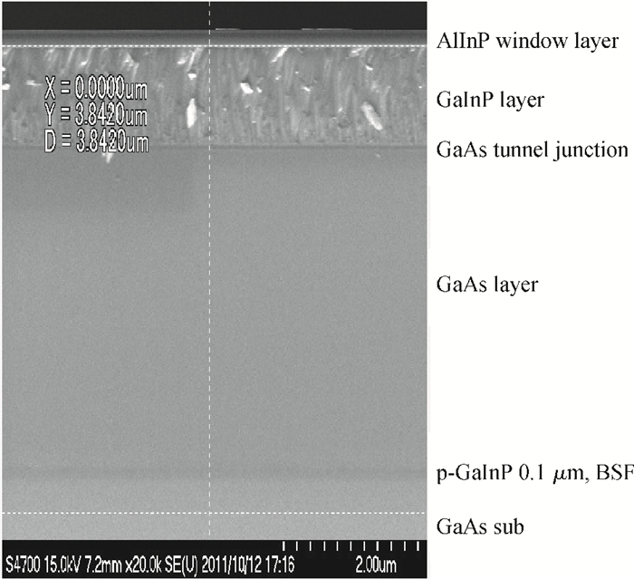
Fig. 1.
Scanning electronic microscopy image of a GaAs/GaInP on solar cell.
SEMICONDUCTOR DEVICES
Pan Dai1, 3, Shulong Lu1, , Lian Ji1, Wei He1, Lifeng Bian1, Hui Yang1, M. Arimochi2, H. Yoshida2, S. Uchida2 and M. Ikeda2
Corresponding author: Lu Shulong, sllu2008@sinano.ac.cn
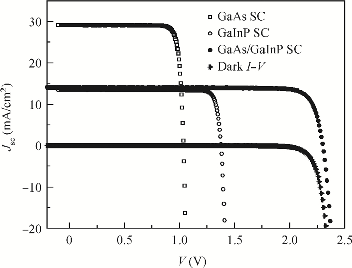
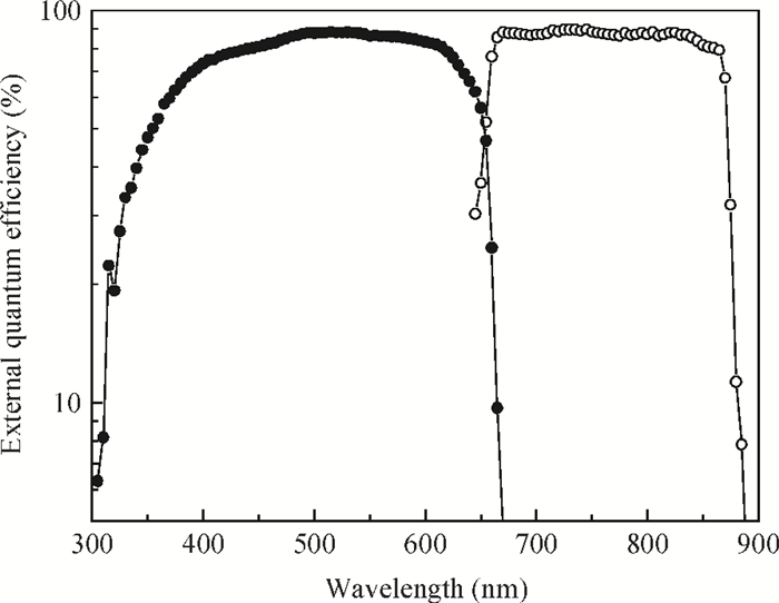
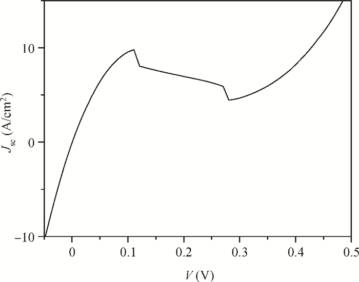
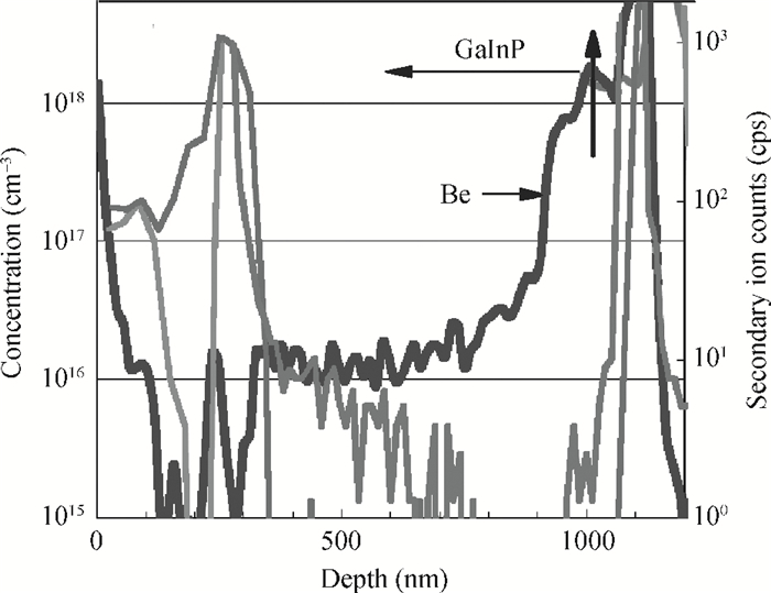
Abstract: We report the recent result of GaAs/GaInP dual-junction solar cells grown by all solid-state molecular-beam-epitaxy (MBE). The device structure consists of a GaIn0.48P homojunction grown epitaxially upon a GaAs homojunction, with an interconnected GaAs tunnel junction. A photovoltaic conversion efficiency of 27% under the AM1.5 globe light intensity is realized for a GaAs/GaInP dual-junction solar cell, while the efficiencies of 26% and 16.6% are reached for a GaAs bottom cell and a GaInP top cell, respectively. The energy loss mechanism of our GaAs/GaInP tandem dual-junction solar cells is discussed. It is demonstrated that the MBE-grown phosphide-containing Ⅲ-Ⅴ compound semiconductor solar cell is very promising for achieving high energy conversion efficiency.
Keywords: molecular beam epitaxy, Ⅲ-Ⅴ semiconductor PN junction, solar cell
| [1] |
Bertness K A, Kurtz S R, Friedman D J, et al. 29.5%-efficient GaInP/GaAs tandem solar cells. Appl Phys Lett, 1994, 65:989 doi: 10.1063/1.112171
|
| [2] |
Takamoto T, Ikeda E, Kurita H, et al. Over 30% efficient InGaP/GaAs tandem solar cells. Appl Phys Lett, 1997, 70:331
|
| [3] |
Garcia I, Rey-Stolle I, Galiana B, et al. A 32.6% efficient lattice-matched dual-junction solar cell working at 1000 suns. Appl Phys Lett, 2009, 94:053509 doi: 10.1063/1.3078817
|
| [4] |
King R R, Law D C, Edmondson K M, et al. 40% efficient metamorphic GaInP/InGaAs/Ge multijunction solar cells. Appl Phys Lett, 2007, 90:183516 doi: 10.1063/1.2734507
|
| [5] |
Kurtz S R, Olson J M, Kibbler A. Modeling of tow-junction, series-connected tandem solar cells using top cell thickness as an adjustable parameter. J Appl Phys, 1990, 68:1890 doi: 10.1063/1.347177
|
| [6] |
Ragay F W, Leys M R, Nouwens P A M, et al. A MBE-grown high-efficiency GaAs solar cell with a directly deposited aluminum front contact. IEEE Electron Device Lett, 1992, 13:618 doi: 10.1109/55.192863
|
| [7] |
Chuang H L, Klausmeier-Brown M E, Melloch M R, et al. Effective minority-carrier hole confinement of Si-doped, n+-n GaAs homojunction barriers. J Appl Phys, 1989, 66:273 doi: 10.1063/1.343868
|
| [8] |
Tobin S P, Vernon C B, Wojtczuk S J, et al. Assessment of MOCVD-and MBE-grown GaAs for high-efficiency solar cell applications. IEEE Trans Electron Devices, 1990, 37:469 doi: 10.1109/16.46385
|
| [9] |
Leinonan P, Pessa M, Haapamaa J, et al. Advances in production MBE grown GaInP/GaAs cascade solar cells. IEEE Xplore-Photovoltaic Specialists Conference, 2000, DOI10.1109/PVSC.2000.916098
|
| [10] |
Wicks G W, Koch M W, Varriano J A, et al. Use of a valved, solid phosphorus source for the growth of Ga0.5In0.5P and Al0.5In0.5P by molecular beam epitaxy. Appl Phys Lett, 1991, 59:342 doi: 10.1063/1.105590
|
| [11] |
Yoon S F, Mah K W, Zheng H Q. Effects of ⅤⅢ ratio on the properties of InGaP grown by a valved phosphorous cracker cell in solid source MBE. Jpn J Appl Phys, 1999, 38:5740 doi: 10.1143/JJAP.38.5740
|
| [12] |
Lu S L, Ji L, He W, et al. High-efficiency GaAs and GaInP solar cells grown by all solid-state molecular-beam-epitaxy. Nanoscale Res Lett, 2011, 6:576 doi: 10.1186/1556-276X-6-576
|
| [13] |
He W, Lu S L, Dong J R, et al. Structural and optical properties of GaInP grown on germanium by metal-organic chemical vapour deposition. Appl Phys Lett, 2010, 97:121909 doi: 10.1063/1.3492854
|
| [14] |
Bauhuis G J, Mulder P, Haverkamp E J, et al. 26.1% thin-film GaAs solar cell using epitaxial lift-off. Solar Energy Materials and Solar Cells, 2009, 93:1488 doi: 10.1016/j.solmat.2009.03.027
|


Article views: 3916 Times PDF downloads: 31 Times Cited by: 0 Times
Received: 01 March 2013 Revised: 19 March 2013 Online: Published: 01 October 2013
| Citation: |
Pan Dai, Shulong Lu, Lian Ji, Wei He, Lifeng Bian, Hui Yang, M. Arimochi, H. Yoshida, S. Uchida, M. Ikeda. A GaAs/GaInP dual junction solar cell grown by molecular beam epitaxy[J]. Journal of Semiconductors, 2013, 34(10): 104006. doi: 10.1088/1674-4926/34/10/104006
****
P Dai, S L Lu, L Ji, W He, L F Bian, H Yang, M. Arimochi, H. Yoshida, S. Uchida, M. Ikeda. A GaAs/GaInP dual junction solar cell grown by molecular beam epitaxy[J]. J. Semicond., 2013, 34(10): 104006. doi: 10.1088/1674-4926/34/10/104006.

|
| [1] |
Bertness K A, Kurtz S R, Friedman D J, et al. 29.5%-efficient GaInP/GaAs tandem solar cells. Appl Phys Lett, 1994, 65:989 doi: 10.1063/1.112171
|
| [2] |
Takamoto T, Ikeda E, Kurita H, et al. Over 30% efficient InGaP/GaAs tandem solar cells. Appl Phys Lett, 1997, 70:331
|
| [3] |
Garcia I, Rey-Stolle I, Galiana B, et al. A 32.6% efficient lattice-matched dual-junction solar cell working at 1000 suns. Appl Phys Lett, 2009, 94:053509 doi: 10.1063/1.3078817
|
| [4] |
King R R, Law D C, Edmondson K M, et al. 40% efficient metamorphic GaInP/InGaAs/Ge multijunction solar cells. Appl Phys Lett, 2007, 90:183516 doi: 10.1063/1.2734507
|
| [5] |
Kurtz S R, Olson J M, Kibbler A. Modeling of tow-junction, series-connected tandem solar cells using top cell thickness as an adjustable parameter. J Appl Phys, 1990, 68:1890 doi: 10.1063/1.347177
|
| [6] |
Ragay F W, Leys M R, Nouwens P A M, et al. A MBE-grown high-efficiency GaAs solar cell with a directly deposited aluminum front contact. IEEE Electron Device Lett, 1992, 13:618 doi: 10.1109/55.192863
|
| [7] |
Chuang H L, Klausmeier-Brown M E, Melloch M R, et al. Effective minority-carrier hole confinement of Si-doped, n+-n GaAs homojunction barriers. J Appl Phys, 1989, 66:273 doi: 10.1063/1.343868
|
| [8] |
Tobin S P, Vernon C B, Wojtczuk S J, et al. Assessment of MOCVD-and MBE-grown GaAs for high-efficiency solar cell applications. IEEE Trans Electron Devices, 1990, 37:469 doi: 10.1109/16.46385
|
| [9] |
Leinonan P, Pessa M, Haapamaa J, et al. Advances in production MBE grown GaInP/GaAs cascade solar cells. IEEE Xplore-Photovoltaic Specialists Conference, 2000, DOI10.1109/PVSC.2000.916098
|
| [10] |
Wicks G W, Koch M W, Varriano J A, et al. Use of a valved, solid phosphorus source for the growth of Ga0.5In0.5P and Al0.5In0.5P by molecular beam epitaxy. Appl Phys Lett, 1991, 59:342 doi: 10.1063/1.105590
|
| [11] |
Yoon S F, Mah K W, Zheng H Q. Effects of ⅤⅢ ratio on the properties of InGaP grown by a valved phosphorous cracker cell in solid source MBE. Jpn J Appl Phys, 1999, 38:5740 doi: 10.1143/JJAP.38.5740
|
| [12] |
Lu S L, Ji L, He W, et al. High-efficiency GaAs and GaInP solar cells grown by all solid-state molecular-beam-epitaxy. Nanoscale Res Lett, 2011, 6:576 doi: 10.1186/1556-276X-6-576
|
| [13] |
He W, Lu S L, Dong J R, et al. Structural and optical properties of GaInP grown on germanium by metal-organic chemical vapour deposition. Appl Phys Lett, 2010, 97:121909 doi: 10.1063/1.3492854
|
| [14] |
Bauhuis G J, Mulder P, Haverkamp E J, et al. 26.1% thin-film GaAs solar cell using epitaxial lift-off. Solar Energy Materials and Solar Cells, 2009, 93:1488 doi: 10.1016/j.solmat.2009.03.027
|

 WeChat ID
Journal of Semiconductors © 2017 All Rights Reserved 京ICP备05085259号-2

 DownLoad:

