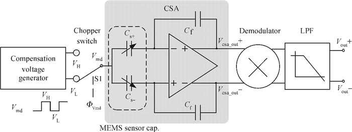
Institute of Electronics, Chinese Academy of Sciences, Beijing 100190, ChinaInstitute of Electronics, Chinese Academy of Sciences, Beijing 100190, China
Abstract: This paper presents a charge-sensitive-amplifier (CSA) based readout circuit for capacitive micro-electro-mechanical-system (MEMS) sensors. A continuous-time (CT) readout structure using the chopper technique is adopted to cancel the low frequency noise and improve the resolution of the readout circuits. An operational trans-conductance amplifier (OTA) structure with an auxiliary common-mode-feedback-OTA is proposed in the fully differential CSA to suppress the chopper modulation induced disturbance at the OTA input terminal. An analog temperature compensation method is proposed, which adjusts the chopper signal amplitude with temperature variation to compensate the temperature drift of the CSA readout sensitivity. The chip is designed and implemented in a 0.35 μm CMOS process and is 2.1×2.1 mm2 in area. The measurement shows that the readout circuit achieves 0.9 aF/√Hz capacitive resolution, 97 dB dynamic range in 100 Hz signal bandwidth, and 0.8 mV/fF sensitivity with a temperature drift of 35 ppm/℃ after optimized compensation.
Modern micro-machined technologies have shown great promise in producing low-cost small sensors with high performance and mass production potential. Capacitive MEMS sensors have shown great advantages of low-power, high-sensitivity and relatively simple structure[1]. For easy comprehension, capacitive sensors can be considered as a simple plate capacitor. The measurand gives excitation on the plate area and the distance between the plates or the permittivity of the insulator between the plates and brings a capacitive change output[2].
The overall MEMS sensor performance is affected by sensor element design and technology, readout circuit and packaging. A high performance MEMS capacitive sensor cannot be developed without a good readout circuit design. Due to the shrinkage of sensor element dimensions, the MEMS sensor output becomes very weak. High performance gyroscopes and accelerometers need sub-aF (10−18 F) level capacitance changes to be resolved by readout circuits[3], which poses a challenge to low-noise readout circuit design. A majority of the reported capacitive MEMS sensor readout circuits adopt the switched-capacitor (SC) topology together with the correlated-double-sampling (CDS) technique to suppress low-frequency noise and improve the resolution. The resolution of an SC charge integration readout circuit is limited by the noise folding and the high KT/C noise[4-6, 11]. The continuous-time (CT) sensing topology has superior noise performance compared to the SC charge integration method[1, 4, 5].
Temperature drift is another critical issue for high resolution MEMS sensor readout circuit design[7-10]. Sensor stability and behavior in temperature variations is crucial to its long-term performance. There are two ways to solve the temperature drift problem. One is to control environment temperature to a constant value, which is outside the operation temperature range, with the help of a power resistor or thermoelectric cooler. However, this method will consume a lot of power and is limited in actual application. The other method is to use a temperature compensation design for the sensor circuit and system. In Ref. [8], polynomial fitting is utilized for micro-gyroscope temperature compensation with the help of an off-chip microprocessor. In Ref. [9], a look-up table is stored in the on-chip EEPROM, containing information relative to the temperature behavior of the sensor. The information is read out and used in a digital correction algorithm to compensate the temperature drift of the output.
Yet up till now few published works have implemented temperature compensation in the analog readout front-end, and instead used a complex digital logic in the back-end. In Ref. [4], a temperature-variable gain amplifier with a gain of about 50 at room temperature is used to compensate the temperature drift. The compensated gyroscope sensitivity typically varies by 1%. However the circuit is subject to high non-linearity because of the open-loop topology of the temperature compensation amplifier. In Ref. [14] a compensated voltage reference is used to perform precise capacitance to frequency conversion and get 23 ppm/℃ temperature coefficient. But the circuit shows high non-linearity and poor readout resolution. In this paper, we demonstrate an analog temperature compensation method based on the CSA readout structure with high resolution, good linearity and low temperature drift.
This paper presents the principle of the CSA-based readout circuits, and the design and implementation of the readout circuits is described in detail. The measurement results and analysis of the readout circuit are also presented.
2.
Theory and analysis
In order to maximize the SNR of the readout circuit, a continuous time voltage (CTV) sensing scheme based on CSA is adopted so that the noise performance is not degraded by the noise folding and switches noise as existing in the switch-capacitor circuits. The proposed readout circuit is consisted of five parts as shown in Fig. 1, including the compensation voltage generator, the chopper switch, the charge sensing amplifier (CSA), demodulator and low-pass filter.
To suppress the low frequency 1/f noise and the dc offset, the chopper stabilization technique is used in CSA-based readout circuits. The chopper technique applies modulation to transport the input signal to a higher frequency where there is no flicker noise by switch S1, and then demodulates it back to the base band after signal processing. The 1/f noise and offset of the circuit are modulated to high frequency and filtered at the output by the low-pass filter. In the chopper technique implementation, a compensation voltage generator with the opposite temperature coefficients against the CSA is designed to compensate the temperature drift of the readout circuit.
2.1
Transfer function
The CSA is shown in Fig. 1, with a differential capacitive sensor represented by capacitors CS+ and CS− connected to the input terminal. The compensation voltage generator gives two voltages: VH and VL. With the help of chopper switch S1, the chopper modulation signal Vmd is generated at the common node of capacitive sensor CS+ and CS−. The CSA generates an amplitude modulated output signal, whose amplitude is Vstep_csa when there is a capacitance difference (CS+ -CS−) at the input. The transfer function of the CSA is
where Vd is the amplitude of the modulation signal Vmd, i.e. (VH -VL)/2, Cf is the integrate capacitor of CSA, and AV is the amplifier open-loop gain. Apparently, a larger Vd and smaller Cf lead to a larger sensitivity for the CSA and help to achieve high resolution. However, Vd amplitude is restricted by the supply voltage and the minimum Cf value is limited by process. In this circuit, Vd is designed to be about 0.9 V at room temperature and Cf to be 1 pF.
The C/V readout sensitivity after demodulation and LPF is affected by the bandwidth of the CSA. The sensitivity after demodulation is given by Eq. (2), in which the upper limit of the modulated CSA output harmonics kcsa is determined by the CSA bandwidth.
where Hcas is transfer function of the CSA, the last two are the harmonics of CSA output and that of the demodulation signal. If the higher frequency harmonics of the modulated CSA output are filtered due to CSA bandwidth limitation, the whole C/V readout sensitivity will be reduced accordingly. After the demodulation, only the elements with frequency far below fchop (i.e. n=m) can pass the LPF and form the final output. For example, if the CSA has an ideal low-pass bandwidth characteristic with cut-off frequency between fchop and 3fchop, then the harmonics more than fchop in the modulated signal are filtered out. The whole C-V sensitivity will be reduced to be 8/π2×Hcsa (about 81%) as a result. In real implementation, the choice of the amplifier bandwidth is decided by power consumption limitation and accuracy requirement. The simulation sensitivity of the proposed circuits is about 0.85 mV/fF.
2.2
Temperature compensation
Equation (1) shows that CSA sensitivity is proportional to the modulation signal amplitude (Vd). So an analog temperature compensation can be realized by designing Vd(T) with a proper temperature characteristic. Considering that the transfer function of CSA Hcsa(T) has a 1st-order temperature coefficient (TC) α1 when Vd is constant (i.e. Vd=Vd0) and can be given by Eq. (3),
Hcsa(T)|Vd=Vd0=Hcsa,0[1+α1(T−T0)],
(3)
where T is chip temperature, T0 is initial room temperature, and Hcsa,0 is CSA sensitivity at T0 with Vd=Vd0.
By making Vd(T) with 1st-order temperature coefficient α2, the compensated transfer function of the CSA is shown in Eq. (4). When α2=−α1, the 1st-order temperature drift of the CSA output can be diminished and the CSA sensitivity is compensated.
In the similar way, if there is a temperature drift in the micro-sensor sensitivity, whose temperature coefficient is α3, 1st-order temperature compensation on the whole system can be accomplished by using a Vd(T) with temperature coefficient α2=−(α1+α3).
2.3
Noise analysis
Since chopper stabilization is employed, the flicker noise can be effectively cancelled as long as that the 1/f noise corner frequency is lower than half of the chopper frequency[11]. Thus the thermal noise is the main noise source to be considered. An equivalent circuit of the CSA is shown in Fig. 2, in which Cp represents the sum of interconnect/ bonding parasitic capacitances and the input capacitance of the input transistors in the amplifier. The two voltage sources ˉvn,md and ˉvn,amp represent the noise of the chopper driving signal and the input referred equivalent noise of the OTA respectively.
Figure
2.
Equivalent circuit of the CSA for noise analysis.
Because of the fully differential structure of the CSA, the noise contribution of the chopper driving signal (ˉvn,md) is proportional to the input capacitance ΔC, which can be regarded as the mismatch of the differential structure. And the noise PSD at the output of the CSA is given by
¯v2n,oΔf=¯v2n,ampΔf(CTCf)2+¯v2n,mdΔf(ΔCinCf)2.
(5)
From Eqs. (5) and (1), the equivalent input capacitance noise of the CSA is thus derived as
where CT is the total capacitance at the amplifier input.
CT=Cs+Cp+Cf.
(7)
Figure 3 gives the contributions of the OTA and the chopper driving signal to the whole CSA noise predicted from Eq. (6) as functions of x=ΔCin/CT. As the curves illustrate, the noise due to the OTA is far larger than that from chopper driving signal, when x is small (i.e. ΔCin is far smaller than Cs and CT), which is the normal condition for linearity consideration when the readout circuit is used to interface the MEMS capacitive sensors. This result helps to lessen the low-noise requirement of the chopper driving signal generator design. From Eq. (6), in order to improve the accuracy of the capacitance measurement, the following approaches should be made: (1) minimize the noise of the OTA, (2) maximize the amplitude of the chopper driving signal Vd, and (3) try to reduce the parasitic capacitance of the bonding wire by single-chip integration, for example.
Figure
3.
Thermal noise contributions from the OTA to the CSA with different x=ΔCin/CT.
The block diagram and schematic of the charge sensing amplifier is shown in Fig. 4. The OTA in the CSA is composed of two parts[12]: the differential mode OTA (DMO) and the common mode OTA (CMO). The DMO serves as the C-V converter with integration capacitor Cf. It consists of a amplify stage and an output common mode feedback (OCMFB) cell. For noise consideration, a telescope structure is employed and the size of the input transistors is properly enlarged. A chopper frequency of 1 MHz at Vmd is chosen which is above twice of the OTA 1/f noise corner frequency. The DMO exhibits a high GBW of 230 MHz and 64 dB open-loop gain, which promises a highly accurate and good linearity C-V conversion.
Figure
4.
(a) Block diagram of the charge sensing amplifier. (b) Schematic of the OTA in the CSA.
Notice that the impedance of the input terminals of the DMO is very high. Their potentials will be unpredictable and vulnerable to interference without proper dc biasing. In this work these nodes are reset to Vicm by Φ1 switch periodically. Such a bias scheme provides a low-impedance dc path with small parasitic capacitance and minimum noise injected by the biasing circuit. The time interval between the reset phase needs to be small enough to ensure that the high impedance node voltage is not evidently affected by charge injection or current leakage. The resetting clock (Φ1) frequency in the proposed circuits is the 1/16 of the chopper frequency.
To suppress the disturbance introduced by the strong chopper carrier, a CMO is adopted as shown in Fig. 4. The CMO is configured in negative feedback topology to stabilize the common mode voltage of the CSA input terminal. The common mode potential at the CSA input is stabilized as in Eq. (7). The CMO needs adequate bandwidth and gain to guarantee an effective virtual short between the DMO input and Vicm, and Ccf is set as large as 20 pF to minimize the disturbance of the chopper signal. In order to enhance the driving capability, a source follower output stage is added to the CMO, of which the GBW exceeds 50 MHz with 20 pF feedback capacitance Ccf.
Vic,CMO=VdCsCs+Ccf(1+Av,CMO)≈VdCsCcfAv,CMO.
(8)
Figure 5 validates the effectiveness of the common mode potential stabilization. When a Vd with 1 MHz frequency and 0.9 V amplitude is applied, the proposed CMO circuits successfully suppress the disturbance of the input common mode potential for the DMO below 400 μV and the output common mode potential below 8 μV, which has little influence on CSA readout circuits.
Figure
5.
Simulation results of the input and output common mode potentials of the CSA.
Figure 6 shows the schematic of the compensation voltage generator, whose structure is normally used as a low-voltage bandgap voltage source. In this paper, it is used to generate chopper voltages Vd= (VH -VL)/2 with a proper temperature coefficient for the chopper modulation signal. Q1, Q2, R1, R2 and M9, M10 compose the core of the current source[15], whose output current is transformed to VH and VL with the help of load resistor R3 and R4. M1-M8 is an OTA used to keep the voltage at nodes A and B equal. The chopper modulation voltage amplitude Vd, which is half of the voltage between VH and VL, and is its temperature coefficient are given in Eqs. (9) and (10).
Vd=VH−VL2=12(VTlnnR1+VBE2R2)R3,
(9)
∂Vd∂T=12(lnnR1kBq+1R2∂VBE2∂T)R3,
(10)
Figure
6.
Schematic of the compensation voltage generator.
where kB is Boltzmann's constant. The terms in Eq. (10) are positive and negative temperature dependent, respectively. By carefully tuning R2, a desired voltage with negative or positive temperature coefficient can be derived. In order to trim the output temperature coefficient, the value of resistor R2 in the circuit is designed to be controlled by 5-bit control code (C). And the value of R2 can be expressed in Eq. (11), in which R2,0 is the normal value of R2, RTRIM is the unit resistor value for trimming, and Cn is the n-th bit of the control signal which is 0 or 1.
R2=R2,0+5∑n=1Cn⋅2n−1⋅RTRIM.
(11)
The temperature compensation simulation results of the whole readout circuit are shown in Fig. 7. With a constant chopper modulation signal, the CSA exhibits a negative temperature dependent sensitivity. Therefore, a positive dependent Vd is needed for compensation. By carefully tuning the compensation voltage generator, an overall readout sensitivity with temperature drift of only 30 ppm/℃ can be obtained, as is shown in Fig. 7(b).
Figure
7.
Simulation results of (a) Vd amplitude and CSA sensitivity versus temperature (normalized to the value at 27 ℃) and (b) readout circuit optimized sensitivity temperature drift.
The demodulator in this paper is implemented with two pairs of switches with a dummy structure[12]. And a 4th-order passive RC LPF is used to filter out the modulated 1/f noise. Between the demodulator and LPF, a pair of switches is added to stop the invalid signal transferring when the reset switch in the CSA is closed (i.e. at Φ1 phase) and avoid an undesirable spike voltage at the output.
4.
Measurements
The readout circuit is designed and implemented in a standard 0.35 μm 2-poly/4-metal CMOS process by Global Foundries. The chip measures 2.1 × 2.1 mm2 and operates with a single 5 V supply. Figure 8 is the micrograph photo of the readout chip with the sub-blocks marked. A temperature sensor is integrated on chip to provide chip temperature information.
Figure
8.
Micrograph of the implemented readout circuit.
The performance of the capacitive readout circuit was verified with two programmable on-chip capacitor arrays connected to the chip input. Figure 9 gives the circuit transient response to a stepwise capacitive input signal with 2 kHz step frequency generated by on-chip capacitor arrays. Figure 10 gives the measurement response of the readout circuit to the input capacitance, while fixing one of the input capacitor array and varying the other in 100 fF steps. The C-V sensitivity of the readout circuit is about 0.8 mV/fF, which is slightly smaller than the simulation result of 0.85 mV/fF due to the fact that the parasitic capacitance at the CSA input terminal degrades the bandwidth of the CSA and reduces the C-V sensitivity. The linear input capacitance range of the readout circuit is about ±700 fF with non-linearity of 0.3%. The linear input/output range is mainly limited by the nested-cascode structure of the charge sensitive amplifier. The bandwidth of the readout circuit is tested and shown in Fig. 11. The -3 dB bandwidth of the readout circuit is larger than 23 kHz, which makes the circuit also suitable for MEMS sensors with high resonant frequency.
Figure
9.
Transient response to stepwise capacitive input.
The readout sensitivities with different temperature compensation control code C are tested and shown in Fig. 12. By carefully tuning the compensation voltage generator, a proper dependent Vd is derived. The temperature drift of the readout sensitivity can be reduced to only 0.0035 mV/fF. In this condition, the temperature coefficient is about 35 ppm/℃, which is reduced by 15 times compared to the uncompensated TC of 550 ppm/℃. At the same time, after compensation the TC of the output offset is about 38 ppm/℃ with constant 400 fF capacitive input. The test results agree with the simulation results and prove the validity of the temperature compensation method in this paper.
Figure
12.
Measured readout circuit sensitivity versus temperature.
Figure 13 shows the measured output noise of the readout circuit, which is about 715 nV/√Hz at 2.5 kHz, corresponding to an input equivalent capacitive noise of 0.9 aF/√Hz. When the circuit is used to readout a capacitive input with 100 Hz signal bandwidth, it can detect a minimum capacitance of 9 aF. So the dynamic range of the readout circuit is larger than 97 dB. The output noise of the circuit without temperature compensation is also given in Fig. 13, in which condition the chopper signal Vmd is generated by off-chip low-noise arbitrary generator AFG3252. Although the proposed temperature compensation method brings some increase in the output noise of the readout circuit, it helps to improve the temperature stability of the circuit and sensor system.
Figure
13.
Measured output noise PSD with/without temperature compensation.
To prove the validity of the proposed readout circuit, it is used to interface a bulk micromachined capacitive-sensing gyroscope[17]. The measured scale factor is about 13 mV/∘/s with a maximum nonlinearity of 0.65‰ over the range of ±200 ∘/s DC rotation, as shown in Fig. 14. The result shows a very good linearity of the readout circuit under small capacitance input. The inset in Fig. 14 gives the microgyroscope response to the step input rotations from ±0.1 ∘/s to ±0.5 ∘/s. The response clearly shows that the gyroscope can resolve input rotation as small as 0.1 ∘/s. Figure 15 shows the typical output noise floor of 123 μV/√Hz around 1 Hz. The noise is almost flat in the low-frequency range from 0.1 to 50 Hz, as shown in Fig. 11, which verifies the 1/f noise suppression of the proposed chopper technique in the CSA. The resolution of the gyroscope can thus be calculated to be about 0.01 ∘/s/√Hz, which proves the low-noise characteristic of the readout circuit. The measured performance of the readout circuits are summarized and compared with previous work as shown in Table 1.
Figure
14.
Scale factor and residual error of the micro-gyroscope with the proposed readout circuit.
A CSA-based readout circuit for MEMS capacitive sensors that simultaneously achieves low-temperature dependence and a low noise floor has been designed in this paper. The proposed readout scheme combines a continuous time readout topology and the chopper technique to reduce the output noise. In addition, an analog temperature compensation method for readout sensitivity has been well validated. The readout circuit achieves a sensitivity of 0.8 mV/fF with temperature dependence as low as 35 ppm/℃, and 97 dB dynamic range with an input referred capacitive noise floor of 0.9 aF/√Hz. The circuit can be used in the capacitive signal readout of high precision MEMS sensors such as gyroscopes and accelerometers. The chip is used to interface an MEMS gyroscope sensor and the measurement results prove the validity and performance of the readout circuit.
Acknowledgment:
The authors wish to thank Professor Jiao Jiwei at the Shanghai Institute of Microsystem and Information Technology, CAS, for the gyroscope sensor elements and test support.
References
[1]
Yazdi N, Kulah H, Najafi K. Precision readout circuits for capacitive micro accelerometers. Proc 3rd IEEE Sensors, Vienna, 2004, 1:28 http://ieeexplore.ieee.org/document/1426091/
[2]
Saukoski M, Aaltonen L, Salo T, et al. Fully integrated charge sensitive amplifier for readout of micromechanical capacitive sensors. IEEE International Symposium on Circuits and Systems (ISACS), Japan, 2005:5377 http://ieeexplore.ieee.org/document/1465851/
[3]
Boser B E. Capacitive interfaces for monolithic integrated sensors. RF Analog-to-Digital Converters, Sensor and Actuator Interfaces, Low-Noise Oscillators, PLLs and Synthesizers, Kluwer, 1997:220 doi: 10.1007%2F978-1-4757-2602-2_9
[4]
Geen J, Sherman S, Chang J, et al. Single chip surface micromachined integrated gyroscope with 50°/h Allan deviation. IEEE J Solid-State Circuits, 2002, 37(12):1860 doi: 10.1109/JSSC.2002.804345
[5]
Wu J, Fedder G K, Carley L R. A low-noise low-offset capacitive sensing amplifier for a 50μg/√Hz monolithic CMOS MEMS accelerometer. IEEE J Solid-State Circuits, 2004, 39(5):722 doi: 10.1109/JSSC.2004.826329
Enz C C, Temes G C. Circuit techniques for reducing the effects of op-amp imperfections:autozeroing, correlated double sampling, and chopper stabilization. Proc IEEE, 1996, 84:1584 doi: 10.1109/5.542410
[12]
Zhang Chong, Wu Qisong, Yin Tao, et al. Noise and mismatch optimization for capacitive MEMS readout. Journal of Semiconductors, 2009, 30(11):115003 doi: 10.1088/1674-4926/30/11/115003
[13]
Aragonés R, Oliver J, Ferrerl C. A 23 ppm/℃ readout circuitry improvement for capacitive sensor acquisition platforms. IEEE 5th International Conference on Sensing Technology, 2011:628
[14]
Dei M, Marchetti E, Bruschi P. A Micro power capacitive sensor readout channel based on the chopper modulation technique. IEEE Prime Conference, 2007:113
[15]
Zhu Z, Wei W, Liu L, et al. A high precision CMOS voltage reference without resistors. Journal of Circuits, Systems, and Computers, 2012, 21(3):1250019 doi: 10.1142/S0218126612500193
[16]
AD7745/AD7746, 24-bit capacitance-to-digital converter with temperature sensor. www. analog. com
[17]
Chen Y, Jiao J, Dong L, et al. Micromachined bar-structure gyroscope with high q-factors for both driving and sensing mode at atmospheric pressure. IEEE 2nd Conference on Sensors Proceedings, Toronto, Canada, Oct, 2003, 1:461
[18]
Ko H, Cho D D. Highly programmable temperature compensated readout circuit for capacitive microaccelerometer. Sensors and Actuators A, 2010, 158:72 doi: 10.1016/j.sna.2009.12.017
Fig. 7.
Simulation results of (a) Vd amplitude and CSA sensitivity versus temperature (normalized to the value at 27 ℃) and (b) readout circuit optimized sensitivity temperature drift.
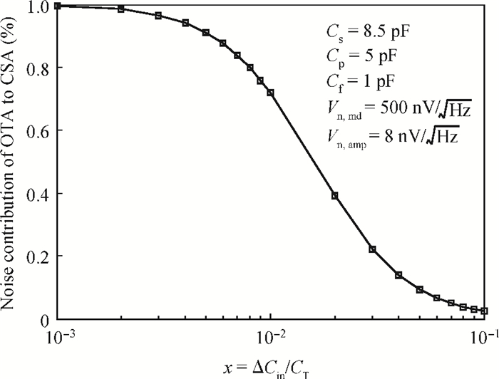
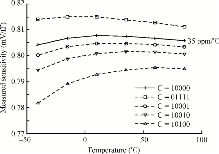
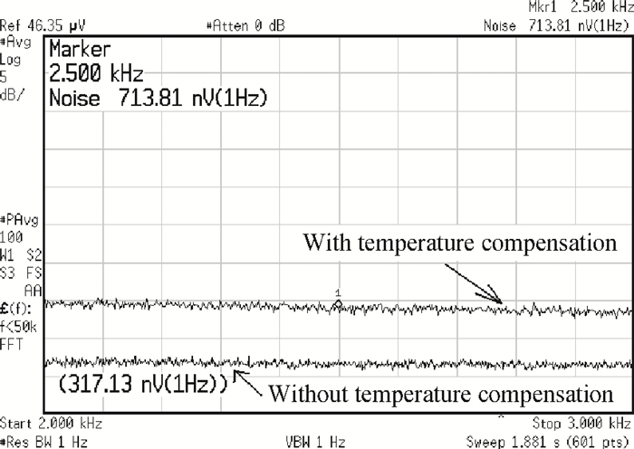
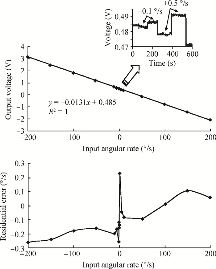
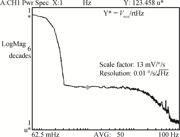
Table 1.
Summary of the readout circuits' specifications and comparison with previous work.
[1]
Yazdi N, Kulah H, Najafi K. Precision readout circuits for capacitive micro accelerometers. Proc 3rd IEEE Sensors, Vienna, 2004, 1:28 http://ieeexplore.ieee.org/document/1426091/
[2]
Saukoski M, Aaltonen L, Salo T, et al. Fully integrated charge sensitive amplifier for readout of micromechanical capacitive sensors. IEEE International Symposium on Circuits and Systems (ISACS), Japan, 2005:5377 http://ieeexplore.ieee.org/document/1465851/
[3]
Boser B E. Capacitive interfaces for monolithic integrated sensors. RF Analog-to-Digital Converters, Sensor and Actuator Interfaces, Low-Noise Oscillators, PLLs and Synthesizers, Kluwer, 1997:220 doi: 10.1007%2F978-1-4757-2602-2_9
[4]
Geen J, Sherman S, Chang J, et al. Single chip surface micromachined integrated gyroscope with 50°/h Allan deviation. IEEE J Solid-State Circuits, 2002, 37(12):1860 doi: 10.1109/JSSC.2002.804345
[5]
Wu J, Fedder G K, Carley L R. A low-noise low-offset capacitive sensing amplifier for a 50μg/√Hz monolithic CMOS MEMS accelerometer. IEEE J Solid-State Circuits, 2004, 39(5):722 doi: 10.1109/JSSC.2004.826329
Enz C C, Temes G C. Circuit techniques for reducing the effects of op-amp imperfections:autozeroing, correlated double sampling, and chopper stabilization. Proc IEEE, 1996, 84:1584 doi: 10.1109/5.542410
[12]
Zhang Chong, Wu Qisong, Yin Tao, et al. Noise and mismatch optimization for capacitive MEMS readout. Journal of Semiconductors, 2009, 30(11):115003 doi: 10.1088/1674-4926/30/11/115003
[13]
Aragonés R, Oliver J, Ferrerl C. A 23 ppm/℃ readout circuitry improvement for capacitive sensor acquisition platforms. IEEE 5th International Conference on Sensing Technology, 2011:628
[14]
Dei M, Marchetti E, Bruschi P. A Micro power capacitive sensor readout channel based on the chopper modulation technique. IEEE Prime Conference, 2007:113
[15]
Zhu Z, Wei W, Liu L, et al. A high precision CMOS voltage reference without resistors. Journal of Circuits, Systems, and Computers, 2012, 21(3):1250019 doi: 10.1142/S0218126612500193
[16]
AD7745/AD7746, 24-bit capacitance-to-digital converter with temperature sensor. www. analog. com
[17]
Chen Y, Jiao J, Dong L, et al. Micromachined bar-structure gyroscope with high q-factors for both driving and sensing mode at atmospheric pressure. IEEE 2nd Conference on Sensors Proceedings, Toronto, Canada, Oct, 2003, 1:461
[18]
Ko H, Cho D D. Highly programmable temperature compensated readout circuit for capacitive microaccelerometer. Sensors and Actuators A, 2010, 158:72 doi: 10.1016/j.sna.2009.12.017
Chinese Journal of Semiconductors , 2005, 26(12): 2445-2448.
Search
GET CITATION
Tao Yin, Chong Zhang, Huanming Wu, Qisong Wu, Haigang Yang. A 97 dB dynamic range CSA-based readout circuit with analog temperature compensation for MEMS capacitive sensors[J]. Journal of Semiconductors, 2013, 34(11): 115005. doi: 10.1088/1674-4926/34/11/115005
T Yin, C Zhang, H M Wu, Q S Wu, H G Yang. A 97 dB dynamic range CSA-based readout circuit with analog temperature compensation for MEMS capacitive sensors[J]. J. Semicond., 2013, 34(11): 115005. doi: 10.1088/1674-4926/34/11/115005.
Export: BibTexEndNote
Share:
Article Metrics
Article views: 2380 TimesPDF downloads: 29 TimesCited by: 0 Times
History
Received: 02 April 2013Revised: 20 May 2013Online:Published: 01 November 2013
Tao Yin, Chong Zhang, Huanming Wu, Qisong Wu, Haigang Yang. A 97 dB dynamic range CSA-based readout circuit with analog temperature compensation for MEMS capacitive sensors[J]. Journal of Semiconductors, 2013, 34(11): 115005. doi: 10.1088/1674-4926/34/11/115005 ****T Yin, C Zhang, H M Wu, Q S Wu, H G Yang. A 97 dB dynamic range CSA-based readout circuit with analog temperature compensation for MEMS capacitive sensors[J]. J. Semicond., 2013, 34(11): 115005. doi: 10.1088/1674-4926/34/11/115005.
Citation:
Tao Yin, Chong Zhang, Huanming Wu, Qisong Wu, Haigang Yang. A 97 dB dynamic range CSA-based readout circuit with analog temperature compensation for MEMS capacitive sensors[J]. Journal of Semiconductors, 2013, 34(11): 115005. doi: 10.1088/1674-4926/34/11/115005
****
T Yin, C Zhang, H M Wu, Q S Wu, H G Yang. A 97 dB dynamic range CSA-based readout circuit with analog temperature compensation for MEMS capacitive sensors[J]. J. Semicond., 2013, 34(11): 115005. doi: 10.1088/1674-4926/34/11/115005.
Institute of Electronics, Chinese Academy of Sciences, Beijing 100190, China
Funds:
Project supported by the National Natural Science Foundation of China (No. 61106025) and the CAS/SAFEA International Partnership Program for Creative Research Teams
the CAS/SAFEA International Partnership Program for Creative Research Teams
the National Natural Science Foundation of China61106025
This paper presents a charge-sensitive-amplifier (CSA) based readout circuit for capacitive micro-electro-mechanical-system (MEMS) sensors. A continuous-time (CT) readout structure using the chopper technique is adopted to cancel the low frequency noise and improve the resolution of the readout circuits. An operational trans-conductance amplifier (OTA) structure with an auxiliary common-mode-feedback-OTA is proposed in the fully differential CSA to suppress the chopper modulation induced disturbance at the OTA input terminal. An analog temperature compensation method is proposed, which adjusts the chopper signal amplitude with temperature variation to compensate the temperature drift of the CSA readout sensitivity. The chip is designed and implemented in a 0.35 μm CMOS process and is 2.1×2.1 mm2 in area. The measurement shows that the readout circuit achieves 0.9 aF/√Hz capacitive resolution, 97 dB dynamic range in 100 Hz signal bandwidth, and 0.8 mV/fF sensitivity with a temperature drift of 35 ppm/℃ after optimized compensation.
Modern micro-machined technologies have shown great promise in producing low-cost small sensors with high performance and mass production potential. Capacitive MEMS sensors have shown great advantages of low-power, high-sensitivity and relatively simple structure[1]. For easy comprehension, capacitive sensors can be considered as a simple plate capacitor. The measurand gives excitation on the plate area and the distance between the plates or the permittivity of the insulator between the plates and brings a capacitive change output[2].
The overall MEMS sensor performance is affected by sensor element design and technology, readout circuit and packaging. A high performance MEMS capacitive sensor cannot be developed without a good readout circuit design. Due to the shrinkage of sensor element dimensions, the MEMS sensor output becomes very weak. High performance gyroscopes and accelerometers need sub-aF (10−18 F) level capacitance changes to be resolved by readout circuits[3], which poses a challenge to low-noise readout circuit design. A majority of the reported capacitive MEMS sensor readout circuits adopt the switched-capacitor (SC) topology together with the correlated-double-sampling (CDS) technique to suppress low-frequency noise and improve the resolution. The resolution of an SC charge integration readout circuit is limited by the noise folding and the high KT/C noise[4-6, 11]. The continuous-time (CT) sensing topology has superior noise performance compared to the SC charge integration method[1, 4, 5].
Temperature drift is another critical issue for high resolution MEMS sensor readout circuit design[7-10]. Sensor stability and behavior in temperature variations is crucial to its long-term performance. There are two ways to solve the temperature drift problem. One is to control environment temperature to a constant value, which is outside the operation temperature range, with the help of a power resistor or thermoelectric cooler. However, this method will consume a lot of power and is limited in actual application. The other method is to use a temperature compensation design for the sensor circuit and system. In Ref. [8], polynomial fitting is utilized for micro-gyroscope temperature compensation with the help of an off-chip microprocessor. In Ref. [9], a look-up table is stored in the on-chip EEPROM, containing information relative to the temperature behavior of the sensor. The information is read out and used in a digital correction algorithm to compensate the temperature drift of the output.
Yet up till now few published works have implemented temperature compensation in the analog readout front-end, and instead used a complex digital logic in the back-end. In Ref. [4], a temperature-variable gain amplifier with a gain of about 50 at room temperature is used to compensate the temperature drift. The compensated gyroscope sensitivity typically varies by 1%. However the circuit is subject to high non-linearity because of the open-loop topology of the temperature compensation amplifier. In Ref. [14] a compensated voltage reference is used to perform precise capacitance to frequency conversion and get 23 ppm/℃ temperature coefficient. But the circuit shows high non-linearity and poor readout resolution. In this paper, we demonstrate an analog temperature compensation method based on the CSA readout structure with high resolution, good linearity and low temperature drift.
This paper presents the principle of the CSA-based readout circuits, and the design and implementation of the readout circuits is described in detail. The measurement results and analysis of the readout circuit are also presented.
2.
Theory and analysis
In order to maximize the SNR of the readout circuit, a continuous time voltage (CTV) sensing scheme based on CSA is adopted so that the noise performance is not degraded by the noise folding and switches noise as existing in the switch-capacitor circuits. The proposed readout circuit is consisted of five parts as shown in Fig. 1, including the compensation voltage generator, the chopper switch, the charge sensing amplifier (CSA), demodulator and low-pass filter.
To suppress the low frequency 1/f noise and the dc offset, the chopper stabilization technique is used in CSA-based readout circuits. The chopper technique applies modulation to transport the input signal to a higher frequency where there is no flicker noise by switch S1, and then demodulates it back to the base band after signal processing. The 1/f noise and offset of the circuit are modulated to high frequency and filtered at the output by the low-pass filter. In the chopper technique implementation, a compensation voltage generator with the opposite temperature coefficients against the CSA is designed to compensate the temperature drift of the readout circuit.
2.1
Transfer function
The CSA is shown in Fig. 1, with a differential capacitive sensor represented by capacitors CS+ and CS− connected to the input terminal. The compensation voltage generator gives two voltages: VH and VL. With the help of chopper switch S1, the chopper modulation signal Vmd is generated at the common node of capacitive sensor CS+ and CS−. The CSA generates an amplitude modulated output signal, whose amplitude is Vstep_csa when there is a capacitance difference (CS+ -CS−) at the input. The transfer function of the CSA is
where Vd is the amplitude of the modulation signal Vmd, i.e. (VH -VL)/2, Cf is the integrate capacitor of CSA, and AV is the amplifier open-loop gain. Apparently, a larger Vd and smaller Cf lead to a larger sensitivity for the CSA and help to achieve high resolution. However, Vd amplitude is restricted by the supply voltage and the minimum Cf value is limited by process. In this circuit, Vd is designed to be about 0.9 V at room temperature and Cf to be 1 pF.
The C/V readout sensitivity after demodulation and LPF is affected by the bandwidth of the CSA. The sensitivity after demodulation is given by Eq. (2), in which the upper limit of the modulated CSA output harmonics kcsa is determined by the CSA bandwidth.
where Hcas is transfer function of the CSA, the last two are the harmonics of CSA output and that of the demodulation signal. If the higher frequency harmonics of the modulated CSA output are filtered due to CSA bandwidth limitation, the whole C/V readout sensitivity will be reduced accordingly. After the demodulation, only the elements with frequency far below fchop (i.e. n=m) can pass the LPF and form the final output. For example, if the CSA has an ideal low-pass bandwidth characteristic with cut-off frequency between fchop and 3fchop, then the harmonics more than fchop in the modulated signal are filtered out. The whole C-V sensitivity will be reduced to be 8/π2×Hcsa (about 81%) as a result. In real implementation, the choice of the amplifier bandwidth is decided by power consumption limitation and accuracy requirement. The simulation sensitivity of the proposed circuits is about 0.85 mV/fF.
2.2
Temperature compensation
Equation (1) shows that CSA sensitivity is proportional to the modulation signal amplitude (Vd). So an analog temperature compensation can be realized by designing Vd(T) with a proper temperature characteristic. Considering that the transfer function of CSA Hcsa(T) has a 1st-order temperature coefficient (TC) α1 when Vd is constant (i.e. Vd=Vd0) and can be given by Eq. (3),
Hcsa(T)|Vd=Vd0=Hcsa,0[1+α1(T−T0)],
(3)
where T is chip temperature, T0 is initial room temperature, and Hcsa,0 is CSA sensitivity at T0 with Vd=Vd0.
By making Vd(T) with 1st-order temperature coefficient α2, the compensated transfer function of the CSA is shown in Eq. (4). When α2=−α1, the 1st-order temperature drift of the CSA output can be diminished and the CSA sensitivity is compensated.
In the similar way, if there is a temperature drift in the micro-sensor sensitivity, whose temperature coefficient is α3, 1st-order temperature compensation on the whole system can be accomplished by using a Vd(T) with temperature coefficient α2=−(α1+α3).
2.3
Noise analysis
Since chopper stabilization is employed, the flicker noise can be effectively cancelled as long as that the 1/f noise corner frequency is lower than half of the chopper frequency[11]. Thus the thermal noise is the main noise source to be considered. An equivalent circuit of the CSA is shown in Fig. 2, in which Cp represents the sum of interconnect/ bonding parasitic capacitances and the input capacitance of the input transistors in the amplifier. The two voltage sources ˉvn,md and ˉvn,amp represent the noise of the chopper driving signal and the input referred equivalent noise of the OTA respectively.
Figure
2.
Equivalent circuit of the CSA for noise analysis.
Because of the fully differential structure of the CSA, the noise contribution of the chopper driving signal (ˉvn,md) is proportional to the input capacitance ΔC, which can be regarded as the mismatch of the differential structure. And the noise PSD at the output of the CSA is given by
Figure 3 gives the contributions of the OTA and the chopper driving signal to the whole CSA noise predicted from Eq. (6) as functions of x=ΔCin/CT. As the curves illustrate, the noise due to the OTA is far larger than that from chopper driving signal, when x is small (i.e. ΔCin is far smaller than Cs and CT), which is the normal condition for linearity consideration when the readout circuit is used to interface the MEMS capacitive sensors. This result helps to lessen the low-noise requirement of the chopper driving signal generator design. From Eq. (6), in order to improve the accuracy of the capacitance measurement, the following approaches should be made: (1) minimize the noise of the OTA, (2) maximize the amplitude of the chopper driving signal Vd, and (3) try to reduce the parasitic capacitance of the bonding wire by single-chip integration, for example.
Figure
3.
Thermal noise contributions from the OTA to the CSA with different x=ΔCin/CT.
The block diagram and schematic of the charge sensing amplifier is shown in Fig. 4. The OTA in the CSA is composed of two parts[12]: the differential mode OTA (DMO) and the common mode OTA (CMO). The DMO serves as the C-V converter with integration capacitor Cf. It consists of a amplify stage and an output common mode feedback (OCMFB) cell. For noise consideration, a telescope structure is employed and the size of the input transistors is properly enlarged. A chopper frequency of 1 MHz at Vmd is chosen which is above twice of the OTA 1/f noise corner frequency. The DMO exhibits a high GBW of 230 MHz and 64 dB open-loop gain, which promises a highly accurate and good linearity C-V conversion.
Figure
4.
(a) Block diagram of the charge sensing amplifier. (b) Schematic of the OTA in the CSA.
Notice that the impedance of the input terminals of the DMO is very high. Their potentials will be unpredictable and vulnerable to interference without proper dc biasing. In this work these nodes are reset to Vicm by Φ1 switch periodically. Such a bias scheme provides a low-impedance dc path with small parasitic capacitance and minimum noise injected by the biasing circuit. The time interval between the reset phase needs to be small enough to ensure that the high impedance node voltage is not evidently affected by charge injection or current leakage. The resetting clock (Φ1) frequency in the proposed circuits is the 1/16 of the chopper frequency.
To suppress the disturbance introduced by the strong chopper carrier, a CMO is adopted as shown in Fig. 4. The CMO is configured in negative feedback topology to stabilize the common mode voltage of the CSA input terminal. The common mode potential at the CSA input is stabilized as in Eq. (7). The CMO needs adequate bandwidth and gain to guarantee an effective virtual short between the DMO input and Vicm, and Ccf is set as large as 20 pF to minimize the disturbance of the chopper signal. In order to enhance the driving capability, a source follower output stage is added to the CMO, of which the GBW exceeds 50 MHz with 20 pF feedback capacitance Ccf.
Figure 5 validates the effectiveness of the common mode potential stabilization. When a Vd with 1 MHz frequency and 0.9 V amplitude is applied, the proposed CMO circuits successfully suppress the disturbance of the input common mode potential for the DMO below 400 μV and the output common mode potential below 8 μV, which has little influence on CSA readout circuits.
Figure
5.
Simulation results of the input and output common mode potentials of the CSA.
Figure 6 shows the schematic of the compensation voltage generator, whose structure is normally used as a low-voltage bandgap voltage source. In this paper, it is used to generate chopper voltages Vd= (VH -VL)/2 with a proper temperature coefficient for the chopper modulation signal. Q1, Q2, R1, R2 and M9, M10 compose the core of the current source[15], whose output current is transformed to VH and VL with the help of load resistor R3 and R4. M1-M8 is an OTA used to keep the voltage at nodes A and B equal. The chopper modulation voltage amplitude Vd, which is half of the voltage between VH and VL, and is its temperature coefficient are given in Eqs. (9) and (10).
where kB is Boltzmann's constant. The terms in Eq. (10) are positive and negative temperature dependent, respectively. By carefully tuning R2, a desired voltage with negative or positive temperature coefficient can be derived. In order to trim the output temperature coefficient, the value of resistor R2 in the circuit is designed to be controlled by 5-bit control code (C). And the value of R2 can be expressed in Eq. (11), in which R2,0 is the normal value of R2, RTRIM is the unit resistor value for trimming, and Cn is the n-th bit of the control signal which is 0 or 1.
The temperature compensation simulation results of the whole readout circuit are shown in Fig. 7. With a constant chopper modulation signal, the CSA exhibits a negative temperature dependent sensitivity. Therefore, a positive dependent Vd is needed for compensation. By carefully tuning the compensation voltage generator, an overall readout sensitivity with temperature drift of only 30 ppm/℃ can be obtained, as is shown in Fig. 7(b).
Figure
7.
Simulation results of (a) Vd amplitude and CSA sensitivity versus temperature (normalized to the value at 27 ℃) and (b) readout circuit optimized sensitivity temperature drift.
The demodulator in this paper is implemented with two pairs of switches with a dummy structure[12]. And a 4th-order passive RC LPF is used to filter out the modulated 1/f noise. Between the demodulator and LPF, a pair of switches is added to stop the invalid signal transferring when the reset switch in the CSA is closed (i.e. at Φ1 phase) and avoid an undesirable spike voltage at the output.
4.
Measurements
The readout circuit is designed and implemented in a standard 0.35 μm 2-poly/4-metal CMOS process by Global Foundries. The chip measures 2.1 × 2.1 mm2 and operates with a single 5 V supply. Figure 8 is the micrograph photo of the readout chip with the sub-blocks marked. A temperature sensor is integrated on chip to provide chip temperature information.
Figure
8.
Micrograph of the implemented readout circuit.
The performance of the capacitive readout circuit was verified with two programmable on-chip capacitor arrays connected to the chip input. Figure 9 gives the circuit transient response to a stepwise capacitive input signal with 2 kHz step frequency generated by on-chip capacitor arrays. Figure 10 gives the measurement response of the readout circuit to the input capacitance, while fixing one of the input capacitor array and varying the other in 100 fF steps. The C-V sensitivity of the readout circuit is about 0.8 mV/fF, which is slightly smaller than the simulation result of 0.85 mV/fF due to the fact that the parasitic capacitance at the CSA input terminal degrades the bandwidth of the CSA and reduces the C-V sensitivity. The linear input capacitance range of the readout circuit is about ±700 fF with non-linearity of 0.3%. The linear input/output range is mainly limited by the nested-cascode structure of the charge sensitive amplifier. The bandwidth of the readout circuit is tested and shown in Fig. 11. The -3 dB bandwidth of the readout circuit is larger than 23 kHz, which makes the circuit also suitable for MEMS sensors with high resonant frequency.
Figure
9.
Transient response to stepwise capacitive input.
The readout sensitivities with different temperature compensation control code C are tested and shown in Fig. 12. By carefully tuning the compensation voltage generator, a proper dependent Vd is derived. The temperature drift of the readout sensitivity can be reduced to only 0.0035 mV/fF. In this condition, the temperature coefficient is about 35 ppm/℃, which is reduced by 15 times compared to the uncompensated TC of 550 ppm/℃. At the same time, after compensation the TC of the output offset is about 38 ppm/℃ with constant 400 fF capacitive input. The test results agree with the simulation results and prove the validity of the temperature compensation method in this paper.
Figure
12.
Measured readout circuit sensitivity versus temperature.
Figure 13 shows the measured output noise of the readout circuit, which is about 715 nV/√Hz at 2.5 kHz, corresponding to an input equivalent capacitive noise of 0.9 aF/√Hz. When the circuit is used to readout a capacitive input with 100 Hz signal bandwidth, it can detect a minimum capacitance of 9 aF. So the dynamic range of the readout circuit is larger than 97 dB. The output noise of the circuit without temperature compensation is also given in Fig. 13, in which condition the chopper signal Vmd is generated by off-chip low-noise arbitrary generator AFG3252. Although the proposed temperature compensation method brings some increase in the output noise of the readout circuit, it helps to improve the temperature stability of the circuit and sensor system.
Figure
13.
Measured output noise PSD with/without temperature compensation.
To prove the validity of the proposed readout circuit, it is used to interface a bulk micromachined capacitive-sensing gyroscope[17]. The measured scale factor is about 13 mV/∘/s with a maximum nonlinearity of 0.65‰ over the range of ±200 ∘/s DC rotation, as shown in Fig. 14. The result shows a very good linearity of the readout circuit under small capacitance input. The inset in Fig. 14 gives the microgyroscope response to the step input rotations from ±0.1 ∘/s to ±0.5 ∘/s. The response clearly shows that the gyroscope can resolve input rotation as small as 0.1 ∘/s. Figure 15 shows the typical output noise floor of 123 μV/√Hz around 1 Hz. The noise is almost flat in the low-frequency range from 0.1 to 50 Hz, as shown in Fig. 11, which verifies the 1/f noise suppression of the proposed chopper technique in the CSA. The resolution of the gyroscope can thus be calculated to be about 0.01 ∘/s/√Hz, which proves the low-noise characteristic of the readout circuit. The measured performance of the readout circuits are summarized and compared with previous work as shown in Table 1.
Figure
14.
Scale factor and residual error of the micro-gyroscope with the proposed readout circuit.
A CSA-based readout circuit for MEMS capacitive sensors that simultaneously achieves low-temperature dependence and a low noise floor has been designed in this paper. The proposed readout scheme combines a continuous time readout topology and the chopper technique to reduce the output noise. In addition, an analog temperature compensation method for readout sensitivity has been well validated. The readout circuit achieves a sensitivity of 0.8 mV/fF with temperature dependence as low as 35 ppm/℃, and 97 dB dynamic range with an input referred capacitive noise floor of 0.9 aF/√Hz. The circuit can be used in the capacitive signal readout of high precision MEMS sensors such as gyroscopes and accelerometers. The chip is used to interface an MEMS gyroscope sensor and the measurement results prove the validity and performance of the readout circuit.
Acknowledgment:
The authors wish to thank Professor Jiao Jiwei at the Shanghai Institute of Microsystem and Information Technology, CAS, for the gyroscope sensor elements and test support.
Yazdi N, Kulah H, Najafi K. Precision readout circuits for capacitive micro accelerometers. Proc 3rd IEEE Sensors, Vienna, 2004, 1:28 http://ieeexplore.ieee.org/document/1426091/
[2]
Saukoski M, Aaltonen L, Salo T, et al. Fully integrated charge sensitive amplifier for readout of micromechanical capacitive sensors. IEEE International Symposium on Circuits and Systems (ISACS), Japan, 2005:5377 http://ieeexplore.ieee.org/document/1465851/
[3]
Boser B E. Capacitive interfaces for monolithic integrated sensors. RF Analog-to-Digital Converters, Sensor and Actuator Interfaces, Low-Noise Oscillators, PLLs and Synthesizers, Kluwer, 1997:220 doi: 10.1007%2F978-1-4757-2602-2_9
[4]
Geen J, Sherman S, Chang J, et al. Single chip surface micromachined integrated gyroscope with 50°/h Allan deviation. IEEE J Solid-State Circuits, 2002, 37(12):1860 doi: 10.1109/JSSC.2002.804345
[5]
Wu J, Fedder G K, Carley L R. A low-noise low-offset capacitive sensing amplifier for a 50μg/√Hz monolithic CMOS MEMS accelerometer. IEEE J Solid-State Circuits, 2004, 39(5):722 doi: 10.1109/JSSC.2004.826329
Enz C C, Temes G C. Circuit techniques for reducing the effects of op-amp imperfections:autozeroing, correlated double sampling, and chopper stabilization. Proc IEEE, 1996, 84:1584 doi: 10.1109/5.542410
[12]
Zhang Chong, Wu Qisong, Yin Tao, et al. Noise and mismatch optimization for capacitive MEMS readout. Journal of Semiconductors, 2009, 30(11):115003 doi: 10.1088/1674-4926/30/11/115003
[13]
Aragonés R, Oliver J, Ferrerl C. A 23 ppm/℃ readout circuitry improvement for capacitive sensor acquisition platforms. IEEE 5th International Conference on Sensing Technology, 2011:628
[14]
Dei M, Marchetti E, Bruschi P. A Micro power capacitive sensor readout channel based on the chopper modulation technique. IEEE Prime Conference, 2007:113
[15]
Zhu Z, Wei W, Liu L, et al. A high precision CMOS voltage reference without resistors. Journal of Circuits, Systems, and Computers, 2012, 21(3):1250019 doi: 10.1142/S0218126612500193
[16]
AD7745/AD7746, 24-bit capacitance-to-digital converter with temperature sensor. www. analog. com
[17]
Chen Y, Jiao J, Dong L, et al. Micromachined bar-structure gyroscope with high q-factors for both driving and sensing mode at atmospheric pressure. IEEE 2nd Conference on Sensors Proceedings, Toronto, Canada, Oct, 2003, 1:461
[18]
Ko H, Cho D D. Highly programmable temperature compensated readout circuit for capacitive microaccelerometer. Sensors and Actuators A, 2010, 158:72 doi: 10.1016/j.sna.2009.12.017
Tao Yin, Chong Zhang, Huanming Wu, Qisong Wu, Haigang Yang. A 97 dB dynamic range CSA-based readout circuit with analog temperature compensation for MEMS capacitive sensors[J]. Journal of Semiconductors, 2013, 34(11): 115005. doi: 10.1088/1674-4926/34/11/115005 ****T Yin, C Zhang, H M Wu, Q S Wu, H G Yang. A 97 dB dynamic range CSA-based readout circuit with analog temperature compensation for MEMS capacitive sensors[J]. J. Semicond., 2013, 34(11): 115005. doi: 10.1088/1674-4926/34/11/115005.
Tao Yin, Chong Zhang, Huanming Wu, Qisong Wu, Haigang Yang. A 97 dB dynamic range CSA-based readout circuit with analog temperature compensation for MEMS capacitive sensors[J]. Journal of Semiconductors, 2013, 34(11): 115005. doi: 10.1088/1674-4926/34/11/115005
****
T Yin, C Zhang, H M Wu, Q S Wu, H G Yang. A 97 dB dynamic range CSA-based readout circuit with analog temperature compensation for MEMS capacitive sensors[J]. J. Semicond., 2013, 34(11): 115005. doi: 10.1088/1674-4926/34/11/115005.
Figure Fig. 1. Block diagram of the readout circuit.
Figure Fig. 2. Equivalent circuit of the CSA for noise analysis.
Figure Fig. 3. Thermal noise contributions from the OTA to the CSA with different x=ΔCin/CT.
Figure Fig. 4. (a) Block diagram of the charge sensing amplifier. (b) Schematic of the OTA in the CSA.
Figure Fig. 5. Simulation results of the input and output common mode potentials of the CSA.
Figure Fig. 6. Schematic of the compensation voltage generator.
Figure Fig. 7. Simulation results of (a) Vd amplitude and CSA sensitivity versus temperature (normalized to the value at 27 ℃) and (b) readout circuit optimized sensitivity temperature drift.
Figure Fig. 8. Micrograph of the implemented readout circuit.
Figure Fig. 9. Transient response to stepwise capacitive input.
Figure Fig. 10. Circuit output versus input differential capacitance.
Figure Fig. 11. The normalized sensitivity amplitude-frequency characteristic of the readout circuit.
Figure Fig. 12. Measured readout circuit sensitivity versus temperature.
Figure Fig. 13. Measured output noise PSD with/without temperature compensation.
Figure Fig. 14. Scale factor and residual error of the micro-gyroscope with the proposed readout circuit.
Figure Fig. 15. Output noise of the micro-gyroscope with the proposed readout circuit.