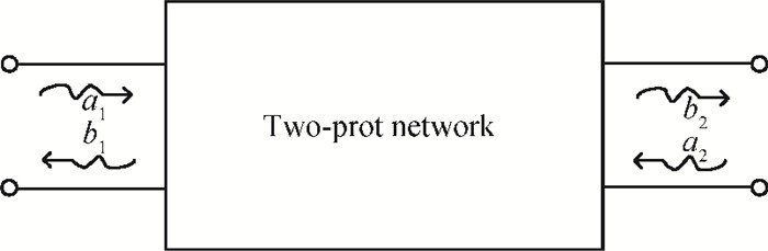
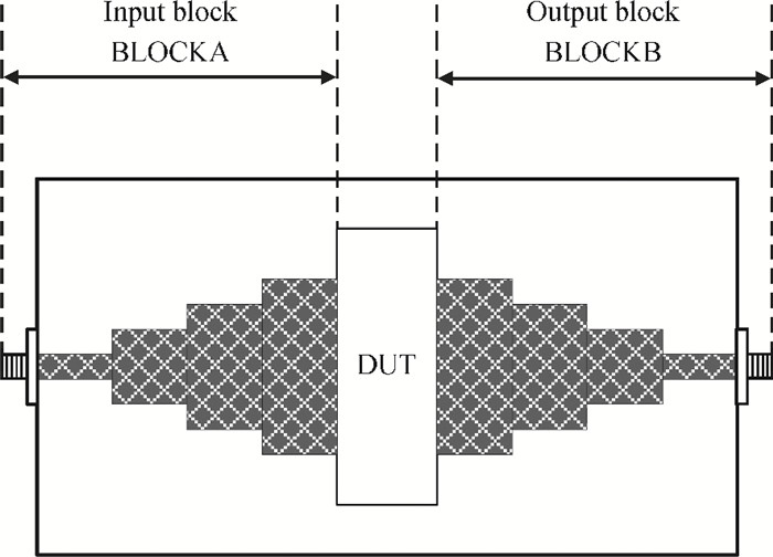
Processing math: 100%
J. Semicond. > 2013, Volume 34 > Issue 3 > 034005

SEMICONDUCTOR DEVICES

A thru-reflect-line calibration for measuring the characteristics of high power LDMOS transistors

Shuai Wang, Ke Li, Yibo Jiang, Mifang Cong, Huan Du and Zhengsheng Han

+ Author Affiliations

 Corresponding author: Han Zhengsheng, Email:zshan@ime.ac.cn

DOI: 10.1088/1674-4926/34/3/034005

PDF

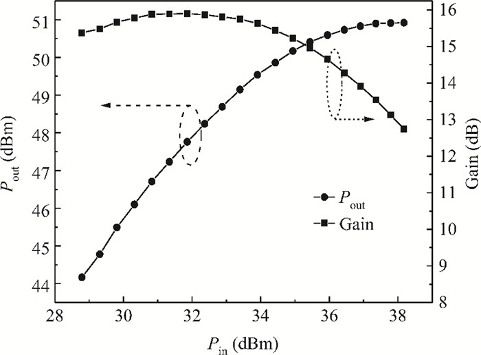
Abstract: The impedance and output power measurements of LDMOS transistors are always a problem due to their low impedance and lead widths. An improved thru-reflect-line (TRL) calibration algorithm for measuring the characteristics of L-band high power LDMOS transistors is presented. According to the TRL algorithm, the individual two-port S parameters of each fixture half can be obtained. By de-embedding these S parameters of the test fixture, an accurate calibration can be made. The improved TRL calibration algorithm is successfully utilized to measure the characteristics of an L-band LDMOS transistor with a 90 mm gate width. The impedance of the transistor is obtained, and output power at 1 dB compression point can reach as much as 109.4 W at 1.2 GHz, achieving 1.2 W/mm power density. From the results, it is seen that the presented TRL calibration algorithm works well.

Key words: thru-reflect-linelateral double-diffused MOSFETlow impedance test fixtureimpedanceoutput power

As the resolution continues to shrink, in order to maintain the depth of focus (DOF), exposure latitude (EL) and minimize the mask error enhancement factor (MEEF) in the meantime, source mask optimization (SMO) has become a key resolution enhancement technique[1-4] that has been widely used for 2x~nm and below technology nodes[3, 4]. ASML's advanced programmable illuminator (FlexRay) and the Tachyon SMO platform enable the optimization of freeform source (FFS) with arbitrary source shapes to cater for different designs of advanced technology node.

SMO has been in the literature since early 1990[5-7]. The primary goal of SMO is to provide the optimum source shape and mask design for a given ideal image[8-10]. The source and mask are typically optimized to improve the process window in terms of the exposure and focus latitude of a process.

Another challenge that has come along is the control of the resist profile, which plays a key role in determining the post-etch CDs. For positive tone development (PTD) process, it is well known that high imaging contrast can help minimize the resist top loss issue in the real process as shown in Fig. 1. To this end, Tachyon has developed the resist-profile-aware SMO[4]. Compared to the POR, the results show that SMO FFS can greatly improve the imaging contrast, enhance focus and exposure latitude, and minimize resist top loss.

Figure  1.  At 2x node, resist top loss and sidewall angle variation.

In this paper, we show a case of 28 nm node with Tachyon's holistic computational lithography solution[11], especially the effectiveness of using resist-aware SMO. The methodology and flow is described in Section 2, mainly introducing the full chip SMO flow. The simulation results with SMO FFS compared with the POR source are shown in Section 3, with applying this flow on 28 nm dark field BEOL layer. Section 4 summarizes the results.

The full chip SMO source optimization flow is shown in Fig. 2. Firstly, SMO is performed on a subset of test clips selected by pattern selection algorithms, which greatly cut the input clip number to achieve a shorter runtime. Then OPC with MB SRAF performs mask correction on the full set of clips with the optimized source. Again LMC checks the litho performance to qualify the source and passed it to full-chip OPC[12-15]. After full-chip OPC and LMC, hotspots are extracted and put back into SMO to begin another round of optimization. Finally the optimized source and mask will be verified in wafer exposure. This iterative flow allows SMO to have a full coverage of all critical patterns, and enlarge the process window within a reasonable turn-around-time. The rest of this paper will elaborate how each component works to reach the final results.

Figure  2.  (Color online) Full chip SMO source optimization flow.

As the first step, pattern selection based on the diffraction order has been proven to be very effective in reducing the SMO runtime while still showing good litho-performance and pattern coverage on full set clips[3].

In this paper, 98 clips in total are provided initially for source optimization, including 84 test clips, 1 SRAM, 1 anchor and 12 BEOL layer hotspots found in POR process. With pattern selection, only 13 clips were selected in SMO for optimization, with 86% reduction in clip number, which are 5 test clips, 1 anchor, 1 SRAM and 6 hotspots. LMC results show that the source optimized by these 13 clips has good pattern coverage on 98 clips in this case, as shown in section 3.

As mentioned previously, Tachyon SMO has the capability to take resist profile into consideration when doing source optimization, so called R3D SMO, as shown in Fig. 3. Similar to the method described in the previous study[4], the edge placement errors (EPE) from both the bottom aerial image (AI) and the top aerial image will be calculated in the SMO cost function, at nominal condition and off nominal conditions, including delta dose, defocus and mask bias. The bottom aerial image plane is defined by the AI location of the SMO input model (pre-calibrated), while the top aerial image plane denoted by top AI location is a user-defined variable in source optimization in order to alleviate the resist top loss.

Figure  3.  (Color online) Using R3D model (optimizing the top and bottom contours) in SMO enables a source that improves CD profile across process window.

After source optimization on 13 clips, Tachyon OPC+ is used to verify the source qualification on a full set of 98 clips in this case. Tachyon OPC+ is a key component of ASML's holistic computational lithography solution, which is based on hybrid image-based and geometry-based dual-engine architecture. Tachyon OPC+ is capable of providing optimal correction with consideration of necking, bridging, contact coverage and other process window limiters at all PW conditions, and compliance with the mask rule check (MRC) user-defined. To further accelerate the turnaround time, Tachyon OPC+ provided a flexible mask optimization (FMO) framework that enables localized OPC correction enhancement based on actual verification results. Fig. 4 shows the FMO's general flow. FMO enables runtime efficient correction by localizing computationally intensive correction techniques to a subset of the full chip layout. In this case, FMO is frequently used to accelerate the turnaround time.

Figure  4.  (Color online) FMO flow.

As shown in Fig. 4, Tachyon LMC is capable of predicting various defects with specific detectors on full chip which are highly likely to be encountered in real wafer process. In this case, LMC is used to check the litho performance with the same specifications on both POR source and SMO FFS. The main detector specifications are necking and bridging detectors with different specifications at nominal and off-conditions. LMC not only serves as a litho performance checking tool, but also feeds SMO and FMO with litho-difficult patterns for iterative optimization as a part of the dynamic flow.

All functional blocks described above compose Tachyon's holistic lithography solution. Particularly, the resist-profile-aware SMO plays an important role in delivering superior results. The lithography performance comparison between POR and SMO FFS is given in the following Section 4.

Standard full-chip OPC and verification applications generally compute only 2D resist contours in a given horizontal resist plane, mostly at the resist bottom. However, it cannot detect resist profile induced patterning problems such as top-loss caused bridging hotspot after etching[16]. Figs. 5 and 6 shows different etch results due to different resist profile, although all patterns have the same bottom resist CD. To resolve these issues, Tachyon platform provides Resist 3D (R3D) profile-aware modeling and supports all computational lithography applications, including OPC and LMC, and it also could be integrated with SMO as mentioned previously.

Figure  5.  (Color online) Resist 3D (R3D) model.
Figure  6.  (Color online) Post-etch CD variation.

The photolithography process can be divided into three stages: exposure, post-bake, and develop. Tachyon FEM+ models these three stages with an optical model, a resist model, and a threshold respectively, plus the following features to simulate the 3D resist profile:

(1) Aerial images are simulated using different resist horizontal plane to get a full overview of light distribution across resist heights. (2) Z diffusion parameter captures the z average of an optical standing wave in the post-bake stage. (3) Resist depth-related thresholds are calibrated to address the different effective developing times through the resist thickness. (4) Surface interaction effects during development are also tunable with dedicated parameters.

Tachyon R3D model calibrates bottom CD measurements along with 3D resist profile information. The input data is easily evaluated with post-etch hot spot and safe spot data[17]. From a baseline 2D model, an R3D model is directly calibrated, together with a SPEC in the form of resist height & CD threshold combination. After calibration, the user gets a single model to simulate contours at different resist heights through the whole process window.

A single compact resist model capable of predicting 3D resist profile is strongly demanded for the advanced technology nodes to avoid the potential hotspots due to imperfect resist pattern shape and its lack of resistance in the subsequent etch process[18].

In this work, we propose a resist 3D (R3D) compact model that takes acid z-diffusion effect into account. The chemical reaction between acid and base along z-direction is treated as a second order effect that is absorbed into the anisotropic diffusion length as a fitting parameter. Meanwhile, the resist model in the x-y wafer plane is still kept in general by applying the compact solution of 2D reaction-diffusion equation.

In order to have the 2D contour predictability at arbitrary resist height, calibrations from entire 3D data (CDs at several heights) are conducted simultaneously with a single cost function so that the R3D compact model is described by a common set of resist free parameters and threshold for all resist heights.

With this benefit, the R3D compact model offers a more physical approach but adds no runtime concern on the OPC and verification applications. The predicted resist cross-section profiles from our test patterns are compared with those computed with rigorous lithography simulator SLITHO and show very good matching results between them.

In this case, 98 clips from N28 BEOL device layer are prepared for source optimization in a dark field PTD process. With pattern selection in SMO, only 13 clips were selected to optimize the source. From the flow in Fig. 3, the first step is to verify the pattern coverage of the source optimized by 13 clips. The PW comparison between selected 13 clips and full 98 clips is shown in Fig. 7. From Fig. 7, DOF@ 5%EL for 13 clips is 146 nm, which is 136 nm for 98 clips, only 7.4% drop at DOF@ 5%EL for the full clip set, which indicates no serious pw limiters in the un-selected clips. The result proves that the 13 clips selected by pattern selection have good pattern coverage on the full clip set.

Figure  7.  (Color online) PW comparison between 13 clips and 98 clips.

To evaluate the SMO FFS performance, more detailed litho-metric comparison between FFS and POR have been made, including overlapped PW, best focus shift (BFS), MEEF and resist top CD. Fig. 8 is the PW comparison between FFS and POR, which shows 23.6% DOF@ 5%EL improvement of FFS over POR, and 45% improvement at maximum exposure latitude. One reason for the big PW improvement is that FFS aligns the best focus of different patterns better. Fig. 9 is the BFS range comparison between FFS and POR. FFS reduces the best focus shift range greatly from 74 to 33 nm, which is a 55% improvement. Furthermore, the worst MEEF from FFS is 7, versus 8 from POR, showing a 12.5% reduction.

Figure  8.  (Color online) PW comparison of POR and FFS.
Figure  9.  (Color online) BFS comparison.

Besides the benefit on OPW and MEEF, one qualified source should also show improvement on resolving resist top loss. To achieve this, the resist profile aware model that can predict the resist top loss is required for the following analysis. Figs. 10 and 11 shows the comparison between SEM picture from real POR process and the contours from calibrated POR model prediction on the same locations, proving that Tachyon FEM+ model can correctly predict the resist top loss issue at the simulation level. Based on such accurate prediction, resist top losses are found on more locations with POR, while all of them can be resolved with FFS, as shown in Fig. 13.

Figure  10.  (Color online) Simulation contours match SEM image.
Figure  11.  (Color online) Top and bottom contour comparison for both POR and FFS.
Figure  13.  AEI SEM image comparison on hotspot 2 for (a) POR and (b) FFS source.

From the comparison as above, FFS shows significant improvement over POR, with key spec shown in Table 1. A simulation qualified source is successfully generated with the resist top-loss taken care of.

Table  1.  Key litho-spec comparison on POR and FFS.
DownLoad: CSV  | Show Table

After a simulation qualified FFS source is delivered by Tachyon SMO, its performance will be verified at the full-chip level. A new OPC model is re-calibrated based on the wafer data exposed by the FFS source. With the new model an OPC recipe is then generated for full chip mask correction. OPC recipe tuning usually requires quite a few iterations to finally meet the specs, with some trivial but delicate adjustments that would cost considerable amount of effort and time. This case, however, shows that using the FFS source helps to ease the pain to meet the verification specs and also reach the repair level with fewer iterations compared with those cost by POR source. The TAT is further reduced by adopting Tachyon FMO to locally repair the rest of the defects. As a result, the tape-out was released ahead of schedule without sacrificing the litho-performance.

Except for the TAT reduction, the improvement of the process window is also validated by wafer data. PWQ wafer was exposed by ASML NXT1950i with multiple dose and focus conditions, using FFS source optimized by Tachyon SMO and mask optimized by Tahcyon OPC. The PWQ results show that full-chip process window is 85 nm @ 5%EL with one single tape-out, which meets the production requirement for N28 M1 (80 nm @ 5%EL). To verify the process window improvement gained by FFS source, at a few weak points and hotspots, AEI SEM images were captured from both POR and SMO FFS wafers. The same scanner of NXT1950i for wafer printing and the same CD-SEM machine were used to rule out machine-to-machine variation. Figs. 12 and 13 show the AEI SEM images of two bridging hotspots as illustrations of the FFS source superior capability in enlarging process window. The SEM images were captured at NC, over-dose 2.5% & defocus ± 30, ± 35, ±40, ± 50, and ± 60 nm. In Fig. 12, serious bridging was found at condition E+2.5% & F ± 30 nm on POR wafer, while with FFS source the bridging began to appear only until the defocus reaches as large as F+60 nm. At another hotspot location shown in Fig. 13 the benefit of using FFS source is even more obvious as all off-condition AEI SEM images are defect-free.

Figure  12.  AEI SEM image comparison on hotspot 1 for (a) POR and (b) FFS source.

In this paper, we evaluate the Tachyon SMO flow with the N28 node to optimize an illumination source for full-chip mask tape-out with Tachyon OPC+. Resist profile aware SMO with pattern selection is adopted to gain both litho-performance and runtime reduction. The simulation results show that the resist top loss issue with POR source can be resolved by FFS optimized by Tachyon SMO. Besides, SMO FFS is also proved effective to enlarge the overlapped PW, lower the worst MEEF and reduce the best focus shift range. In the N28 M1 case, FFS shows 23.6% improvement on DOF @ 5%EL, 12.5% reduction on worst MEEF and 55.4% reduction on BFS range over POR at the simulation level. Meanwhile, the adoption of the FFS source helps reduce the TAT by making the OPC recipe tuning easier and finally achieving the tape-out ahead of schedule without sacrificing the quality. The process window improvement gained from Tachyon SMO FFS is also verified on wafer. The bridging defects, as an example, appeared at 50 nm defocus with the POR source are successfully resolved with SMO FFS. The full-chip PWQ shows a process window of 85~nm @ 5%EL with one single tape-out, which meets the industry process window requirement for N28 M1 (80 nm @ 5%EL).

Acknowledgements: The authors would like to thank ASML BRION FE and PWE team for their effective support on HLMC N28 process development.


[1]
Ma R, Han G, Chen X, et al. Calibrating an arbitrary test fixture for a symmetric device by three measurements. IEEE Trans Instrumentation Measurement, 2010, 59(1):145 doi: 10.1109/TIM.2009.2022111
[2]
Engen G F, Hoer C A. Thru-reflect-line:an improved technique for calibrating the dual six-port automatic network analyzer. IEEE Trans Microw Theory Tech, 1979, 27(12):987 doi: 10.1109/TMTT.1979.1129778
[3]
Ludwig R, Bretchko P. RF circuit design:theory and applications. Upper Saddle River:Prentice-Hall, 2000 http://ci.nii.ac.jp/ncid/BA48143667
[4]
Aaen P, Pla J, Bridges D, et al. A wideband method for the rigorous low-impedance loadpull measurement of high-power transistors suitable for large-signal model validation. ARFTG Conference Digest-Fall, 2000, 38:1 http://ieeexplore.ieee.org/document/4120134/?reload=true&arnumber=4120134&contentType=Conference%20Publications
[5]
Bouny J J. Impedance measurements for high power RF transistors using the TRL method. Microwave Journal, 1999, 42(10):126
[6]
Aboush Z, Jones C, Knight G, et al. High power active harmonic load-pull system for characterization of high power 100-watt transistors. Microwave Conference, 2005, 1:4 http://ieeexplore.ieee.org/document/1608930/keywords
[7]
Pozar D M. Microwave engineering. 3rd ed. New York: John Wiley & Sons, 2005
[8]
Klopfenstein R W. A transmission line taper of improved design. Proc IRE, 1956, 44(1):31 doi: 10.1109/JRPROC.1956.274847
[9]
Shih C. Advanced TRL (through-reflect-line) fixture design and error analyses for RF high power transistor characterization and automatic load pull measurement. ARFTG Conference Digest-Spring, 1998, 33:72 http://ieeexplore.ieee.org/document/4119969/keywords
Fig. 1.  Test fixture model.

Fig. 2.  Two ports network.

Fig. 3.  Schematic diagram of the reflection standard measurement.

Fig. 4.  Low impedance TRL test fixture.

Fig. 5.  Comparison between the measured S22 results of the taper impedance and the simulation.

Fig. 6.  Calibration results of the thru standards.

Fig. 7.  Load-pull test results.

Table 1.   Impedances of the LDMOS transistor in the specified working conditions.

[1]
Ma R, Han G, Chen X, et al. Calibrating an arbitrary test fixture for a symmetric device by three measurements. IEEE Trans Instrumentation Measurement, 2010, 59(1):145 doi: 10.1109/TIM.2009.2022111
[2]
Engen G F, Hoer C A. Thru-reflect-line:an improved technique for calibrating the dual six-port automatic network analyzer. IEEE Trans Microw Theory Tech, 1979, 27(12):987 doi: 10.1109/TMTT.1979.1129778
[3]
Ludwig R, Bretchko P. RF circuit design:theory and applications. Upper Saddle River:Prentice-Hall, 2000 http://ci.nii.ac.jp/ncid/BA48143667
[4]
Aaen P, Pla J, Bridges D, et al. A wideband method for the rigorous low-impedance loadpull measurement of high-power transistors suitable for large-signal model validation. ARFTG Conference Digest-Fall, 2000, 38:1 http://ieeexplore.ieee.org/document/4120134/?reload=true&arnumber=4120134&contentType=Conference%20Publications
[5]
Bouny J J. Impedance measurements for high power RF transistors using the TRL method. Microwave Journal, 1999, 42(10):126
[6]
Aboush Z, Jones C, Knight G, et al. High power active harmonic load-pull system for characterization of high power 100-watt transistors. Microwave Conference, 2005, 1:4 http://ieeexplore.ieee.org/document/1608930/keywords
[7]
Pozar D M. Microwave engineering. 3rd ed. New York: John Wiley & Sons, 2005
[8]
Klopfenstein R W. A transmission line taper of improved design. Proc IRE, 1956, 44(1):31 doi: 10.1109/JRPROC.1956.274847
[9]
Shih C. Advanced TRL (through-reflect-line) fixture design and error analyses for RF high power transistor characterization and automatic load pull measurement. ARFTG Conference Digest-Spring, 1998, 33:72 http://ieeexplore.ieee.org/document/4119969/keywords
1

Performance analysis of SiGe double-gate N-MOSFET

A. Singh, D. Kapoor, R. Sharma

Journal of Semiconductors, 2017, 38(4): 044003. doi: 10.1088/1674-4926/38/4/044003

2

The impact of gate misalignment on the analog performance of a dual-material double gate junctionless transistor

S. Intekhab Amin, R. K. Sarin

Journal of Semiconductors, 2015, 36(9): 094001. doi: 10.1088/1674-4926/36/9/094001

3

Modeling the drain current and its equation parameters for lightly doped symmetrical double-gate MOSFETs

Mini Bhartia, Arun Kumar Chatterjee

Journal of Semiconductors, 2015, 36(4): 044003. doi: 10.1088/1674-4926/36/4/044003

4

Modeling of subthreshold characteristics for undoped and doped deep nanoscale short channel double-gate MOSFETs

Jin Xiaoshi, Liu Xi, Wu Meile, Chuai Rongyan, Jung-Hee Lee, et al.

Journal of Semiconductors, 2012, 33(12): 124003. doi: 10.1088/1674-4926/33/12/124003

5

Effect of underlap and gate length on device performance of an AlInN/GaN underlap MOSFET

Hemant Pardeshi, Sudhansu Kumar Pati, Godwin Raj, N Mohankumar, Chandan Kumar Sarkar, et al.

Journal of Semiconductors, 2012, 33(12): 124001. doi: 10.1088/1674-4926/33/12/124001

6

Analytical modeling of drain current and RF performance for double-gate fully depleted nanoscale SOI MOSFETs

Rajiv Sharma, Sujata Pandey, Shail Bala Jain

Journal of Semiconductors, 2012, 33(2): 024001. doi: 10.1088/1674-4926/33/2/024001

7

Gate current modeling and optimal design of nanoscale non-overlapped gate to source/drain MOSFET

Ashwani K. Rana, Narottam Chand, Vinod Kapoor

Journal of Semiconductors, 2011, 32(7): 074001. doi: 10.1088/1674-4926/32/7/074001

8

A 3.125-Gb/s inductorless transimpedance amplifier for optical communication in 0.35 μm CMOS

Xu Hui, Feng Jun, Liu Quan, Li Wei

Journal of Semiconductors, 2011, 32(10): 105003. doi: 10.1088/1674-4926/32/10/105003

9

Frequency of the transition spectral line of an electron in quantum rods

Wang Guiwen, Xiao Jinglin

Journal of Semiconductors, 2010, 31(9): 092002. doi: 10.1088/1674-4926/31/9/092002

10

Impedance hygrometer based on cellulose and CuPc

Kh. S. Karimov, T. A. Qasuria, Zubair Ahmad

Journal of Semiconductors, 2010, 31(6): 064011. doi: 10.1088/1674-4926/31/6/064011

11

A low power cyclic ADC design for a wireless monitoring system for orthopedic implants

Chen Yi, Li Fule, Chen Hong, Zhang Chun, Wang Zhihua, et al.

Journal of Semiconductors, 2009, 30(8): 085009. doi: 10.1088/1674-4926/30/8/085009

12

1-Gb/s zero-pole cancellation CMOS transimpedance amplifier for Gigabit Ethernet applications

Huang Beiju, Zhang Xu, Chen Hongda

Journal of Semiconductors, 2009, 30(10): 105005. doi: 10.1088/1674-4926/30/10/105005

13

Experimental Study on Solar Cell Arrays of Trough Concentrating Solar System

Xu Yongfeng, Li Ming, Wang Liuling, He Jianhua, Zhang Xinghua, et al.

Journal of Semiconductors, 2008, 29(12): 2421-2426.

14

Fabrication and Characteristics of Nano-Aperture Vertical-Cavity Surface-Emitting Laser

Gao Jianxia, Song Guofeng, Gan Qiaoqiang, Xu Yun, Guo Baoshan, et al.

Chinese Journal of Semiconductors , 2007, 28(2): 265-268.

15

A Low-Power High-Frequency CMOS Peak Detector

Li Xuechu, Gao Qingyun, Qin Shicai

Chinese Journal of Semiconductors , 2006, 27(10): 1707-1710.

16

Effect of Relaxation Time on Electron Transport Properties in Double-Barrier Structures

Dai Zhenhong, Ni Jun

Chinese Journal of Semiconductors , 2006, 27(4): 604-608.

17

Influence of Polarization-Induced Electric Fields on Optical Properties of Intersubband Transitions in AlxGa1-xN/GaN Double Quantum Wells

Lei Shuangying, Shen Bo, Xu Fujun, Yang Zhijian, Xu Ke, et al.

Chinese Journal of Semiconductors , 2006, 27(3): 403-408.

18

A 2.4GHz Low Power ASK Transmitter for Wireless Capsule Endoscope Applications

Han Shuguang, Chi Baoyong, Wang Zhihua

Chinese Journal of Semiconductors , 2006, 27(6): 988-993.

19

Synthesis and Characterization of SiCOF/a-C∶F Double-Layer Films with Low Dielectric Constant for Copper Interconnects

Zhang Wei, Zhu Lian, Sun Qingqing, Lu Hongliang, Ding Shijin, et al.

Chinese Journal of Semiconductors , 2006, 27(3): 429-433.

20

Analysis of Characteristic Impedance and Effective Dielectric Constant of Asymmetrical Coplanar Waveguide with Finite Dimensions

Chinese Journal of Semiconductors , 2000, 21(8): 739-743.

  • Search

    Advanced Search >>

    GET CITATION

    Shuai Wang, Ke Li, Yibo Jiang, Mifang Cong, Huan Du, Zhengsheng Han. A thru-reflect-line calibration for measuring the characteristics of high power LDMOS transistors[J]. Journal of Semiconductors, 2013, 34(3): 034005. doi: 10.1088/1674-4926/34/3/034005
    S Wang, K Li, Y B Jiang, M F Cong, H Du, Z S Han. A thru-reflect-line calibration for measuring the characteristics of high power LDMOS transistors[J]. J. Semicond., 2013, 34(3): 034005. doi: 10.1088/1674-4926/34/3/034005.
    shu

    Export: BibTex EndNote

    Article Metrics

    Article views: 3289 Times PDF downloads: 56 Times Cited by: 0 Times

    History

    Received: 20 August 2012 Revised: 14 September 2012 Online: Published: 01 March 2013

    Catalog

      Email This Article

      User name:
      Email:*请输入正确邮箱
      Code:*验证码错误
      Shuai Wang, Ke Li, Yibo Jiang, Mifang Cong, Huan Du, Zhengsheng Han. A thru-reflect-line calibration for measuring the characteristics of high power LDMOS transistors[J]. Journal of Semiconductors, 2013, 34(3): 034005. doi: 10.1088/1674-4926/34/3/034005 ****S Wang, K Li, Y B Jiang, M F Cong, H Du, Z S Han. A thru-reflect-line calibration for measuring the characteristics of high power LDMOS transistors[J]. J. Semicond., 2013, 34(3): 034005. doi: 10.1088/1674-4926/34/3/034005.
      Citation:
      Shuai Wang, Ke Li, Yibo Jiang, Mifang Cong, Huan Du, Zhengsheng Han. A thru-reflect-line calibration for measuring the characteristics of high power LDMOS transistors[J]. Journal of Semiconductors, 2013, 34(3): 034005. doi: 10.1088/1674-4926/34/3/034005 ****
      S Wang, K Li, Y B Jiang, M F Cong, H Du, Z S Han. A thru-reflect-line calibration for measuring the characteristics of high power LDMOS transistors[J]. J. Semicond., 2013, 34(3): 034005. doi: 10.1088/1674-4926/34/3/034005.

      A thru-reflect-line calibration for measuring the characteristics of high power LDMOS transistors

      DOI: 10.1088/1674-4926/34/3/034005
      More Information
      • Corresponding author: Han Zhengsheng, Email:zshan@ime.ac.cn
      • Received Date: 2012-08-20
      • Revised Date: 2012-09-14
      • Published Date: 2013-03-01

      Catalog

        /

        DownLoad:  Full-Size Img  PowerPoint
        Return
        Return