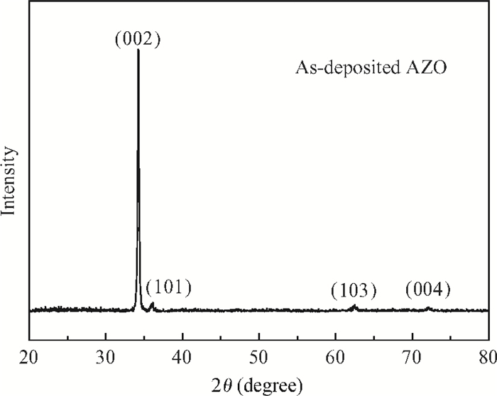
J. Semicond. > 2013, Volume 34 > Issue 6 > 063004

SEMICONDUCTOR MATERIALS

Development of aluminum-doped ZnO films for a-Si:H/μc-Si:H solar cell applications

Zhifang Lei, Guangyu Chen, Shibin Gu, Lingling Dai, Rong Yang, Yuan Meng, Ted Guo and Liwei Li

+ Author Affiliations

 Corresponding author: Li Liwei, Email:liliwei@enn.cn

DOI: 10.1088/1674-4926/34/6/063004

PDF

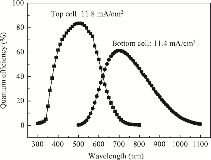
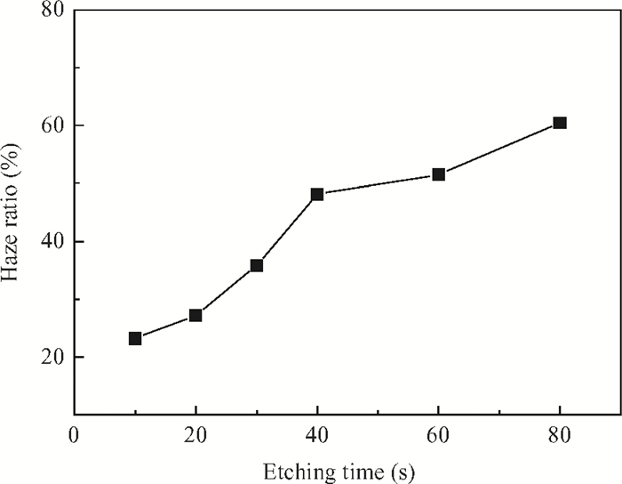
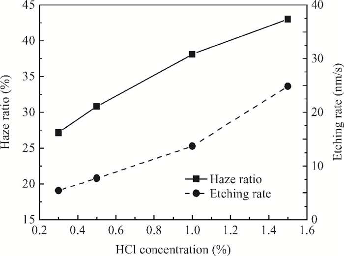
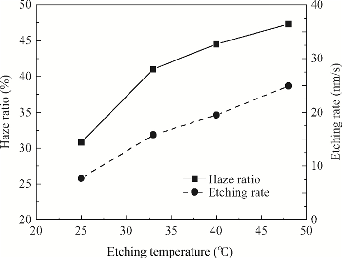
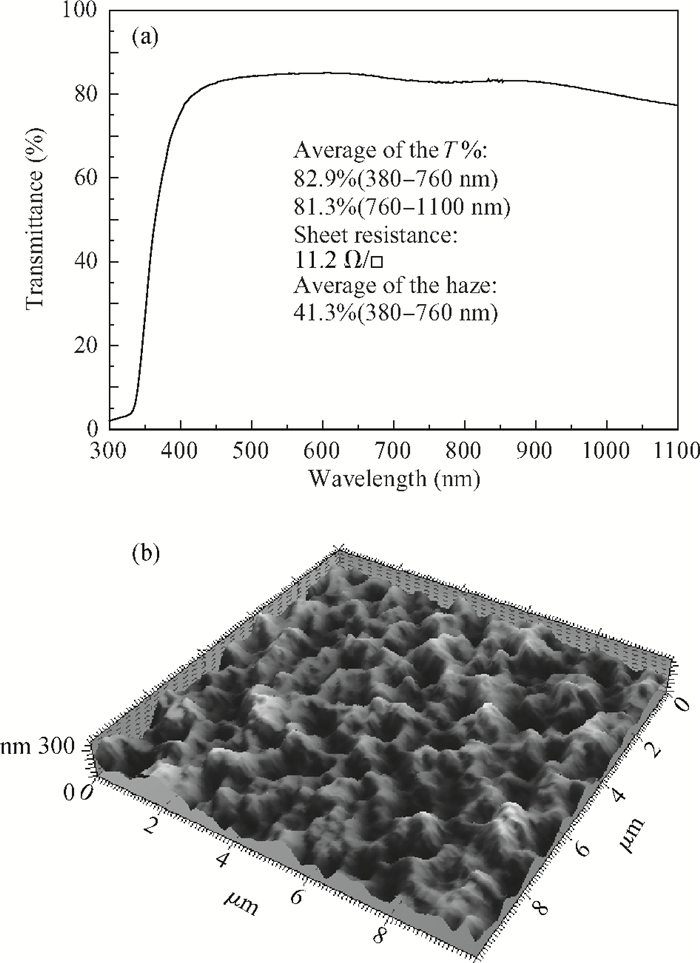
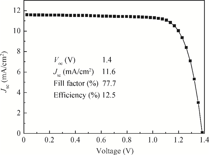
Abstract: This study deals with the optimization of direct current (DC) sputtered aluminum-doped zinc oxide (AZO) thin films and their incorporation into a-Si:H/μc-Si:H tandem junction thin film solar cells aiming for high conversion efficiency. Electrical and optical properties of AZO films, i.e. mobility, carrier density, resistivity, and transmittance, were comprehensively characterized and analyzed by varying sputtering deposition conditions, including chamber pressure, substrate temperature, and sputtering power. The correlations between sputtering processes and AZO thin film properties were first investigated. Then, the AZO films were textured by diluted hydrochloric acid wet etching. Through optimization of deposition and texturing processes, AZO films yield excellent electrical and optical properties with a high transmittance above 81% over the 380-1100 nm wavelength range, low sheet resistance of 11 Ω/$\square$ and high haze ratio of 41.3%. In preliminary experiments, the AZO films were applied to a-Si:H/μc-Si:H tandem thin film solar cells as front contact electrodes, resulting in an initial conversion efficiency of 12.5% with good current matching between subcells.

Key words: aluminum-doped zinc oxidemagnetron sputteringtandem silicon thin film solar cell

Transparent conductive oxide (TCO) thin films have a wide range of applications in the photovoltaic (PV) industry. As a transparent electrode material, TCO has to provide high light transparency, low electrical resistance, and strong capability of light scattering. Currently fluorine-doped tin oxide (SnO$_{2}$:F or FTO) films are widely used as TCO films in the PV industry. However, as an alternative approach, aluminum doped zinc oxide (ZnO:Al or AZO) film, which can be produced on large areas in a controllable manner by magnetron sputtering, is considered as a substitute for use in amorphous silicon solar cells. Compared to well established FTO films by chemical vapor deposition (CVD), AZO films maintain good stability in ambient hydrogen plasma[1, 2], lower resistivity, less absorption, and improved light scattering thanks to the fact that a precise control of the morphology can be achieved from the wet chemical etching process[3-5]. In particular, in a-Si:H/$\mu $c-Si:H tandem thin film solar cells, AZO has a better performance in increasing the short circuit current, reducing silicon thickness, and lowering down the production cost of solar modules[6, 7].

So far, among various deposition processes, magnetron sputtering is one of the most promising methods for ZnO deposition owing to the inherent ease with which the deposition conditions can be controlled well[8]. In this study, AZO thin films were prepared by a DC sputtering system with ZnO:Al$_{2}$O$_{3}$ ceramic targets, and the correlations between the sputtering processes and properties of AZO thin films were established. AZO thin films with high transmittance, high light scattering, and low electrical resistivity were obtained through the optimization of sputtering processes. As a result, the AZO thin films were incorporated into a-Si:H/$\mu $c-Si:H thin film solar cells, and an initial conversion efficiency up to 12.5% has been achieved in preliminary experiments.

AZO thin films were deposited by a high vacuum magnetron sputtering system on 3.2 mm thick, 140 $\times$ 140 mm$^{2}$ sized low iron glass substrates using ceramic targets with an Al$_{2}$O$_{3}$-concentration of 1 wt%. The deposition pressure was adjusted through Ar gas flow; the substrate temperature was pre-calibrated on 3.2 mm thick glass with a thermal sensor and controlled by heater temperature during film deposition, and the film thickness was controlled by sputtering power and deposition time. Then, the as-deposited AZO thin films were textured by wet-chemical etching with diluted hydrochloric acid (HCl). The surface morphology was controlled by etchant concentration, etching time, and temperature. Immediately after the chemical etching process the samples were cleaned by D.I. water. Finally, the glass substrates with textured AZO were used to fabricate Si thin film solar cells. The a-Si:H/$\mu $c-Si:H tandem junctions were prepared using a plasma-enhanced chemical vapor deposition (PECVD) system, followed by AZO/Ag back electrodes that were formed by sputtering with a shadow mask to define a small cell area around 0.5 cm$^{2}$.

Electrical resistivity of the AZO films was tested by a four-point probe meter (RTS-9). Hall mobility and carrier concentration, were measured by a Hall meter (Ecopia, HMS-2000). Transmittance and haze of the films were measured using a UV/VIS spectrometer (Perkin Elmer, Lambda 750) in the wavelength range of 300-1100 nm. Film thickness was scanned by a surface profiler (KLA, P-16+). Surface morphology was inspected by an atomic force microscopy (AFM) (Agilent, 5400 SPM). The crystal structure of the thin films was investigated using X-ray diffraction (XRD, Bruker advance D8) with Cu K$\alpha$ radiation ($\lambda$ $=$ 0.1540 nm). Current-voltage (IV) and quantum-efficiency (QE) characteristics of solar cells were tested at standard testing conditions (AM1.5, 100 mW/cm$^{2}$, 25 ℃).

Figure 1 shows the typical XRD pattern of the AZO thin film with a thickness of $\sim $860 nm. It can be found that the film has a hexagonal wurtzite crystal structure (P63mc). In this work, all the deposited films have prominent $\langle$002$\rangle$ orientation as is observed from the XRD spectra, indicating a preferential $c$-axis orientation perpendicular to the substrate[9].

Figure  1.  X-ray diffraction pattern for the AZO film.

AZO thin films were sputtered with a similar thickness around 860 nm with the deposition temperature varied as other sputtering conditions are fixed. Then the electrical and optical properties were analyzed. The dependence of carrier concentration ($n)$, Hall mobility ($\mu$), and electrical resistivity ($\rho$) on deposition temperature is shown in Fig. 2(a). It is observed that carrier concentration lies in a narrow range of (4-5) $\times$ 10$^{20}$ cm$^{-3}$, showing a weak dependence on deposition temperature. The Hall mobility shows an initial sharp rise and then a gradual decrease as the deposition temperature further increases. Co-determined by carrier concentration and mobility, electrical resistivity shows a minimum value at an intermediate temperature. The above data can be interpreted as follows: (1) a higher deposition temperature can enhance film crystallization, increase grain sizes, and reduce defects, resulting in better Hall mobility due to less carrier scattering and trapping; (2) A too high deposition temperature leads to excess increase of Al precipitation at grain boundaries in the form of Al$_{2}$O$_{3}$, which causes variation of grain orientation, increases scattering, and thus reduces carrier mobility[10, 11]. Both factors work together and co-determine that minimal electrical resistivity occurs at the intermediate temperature.

Figure  2.  (a) Carrier concentration ($n$), Hall mobility ($\mu$), and electrical resistivity ($\rho$) versus deposition temperature. (b) Spectral transmittance versus deposition temperature.

Figure 2(b) shows the optical transmittance in the UV-VIS range of AZO films deposited at different deposition temperatures, with sputtering pressure and deposition power fixed. By increasing the deposition temperature, the transmittance increases in the short wavelength range (340-450 nm), and then reaches saturation at an intermediate temperature. As mentioned above, temperature increase leads to higher carrier concentration and wider optical bandgap, which shortens the 'cutoff' wavelength of light absorption, leading to a higher transmittance in the short wavelength range[10, 11].

Effects of sputtering pressure on AZO properties were plotted in Fig. 3. As shown in Fig. 3(a), sputtering pressure plays a negligible role in carrier concentration in the whole pressure range examined in this study. However, Hall mobility has a decreasing trend with increase of sputtering pressure, especially in the higher pressure range. Accordingly, electrical resistivity basically remains at a low level of 4 $\times$ 10$^{-4}$$\Omega$$\cdot$cm at the lower pressure range, but evidently increases after that. This may be explained by less collision among sputtered atoms and argon ions, and thus less energy loss at a low sputtering pressure. Higher energy of sputtering species helps improve the crystallization of the AZO film, resulting in less carrier scattering and thus higher mobility. At a higher sputtering pressure, a higher probability of collision between argon ions and sputtered atoms results in more energy loss when the atoms reach the substrate surface, which degrades the crystallization of the AZO film, leading to lower mobility and higher resistivity[12, 13].

Figure  3.  (a) Carrier concentration ($n$), Hall mobility ($\mu$) and electrical resistivity ($\rho$) versus sputtering pressure. (b) Spectral transmittance versus sputtering pressure. (Deposition temperature and sputtering power were fixed, and AZO thickness is $\sim$860 nm).

Sputtering pressure shows very minor effects on transmittance of AZO films as illustrated in Fig. 3(b). As mentioned earlier, AZO optical properties are considerably dominated by Al concentration, which is not sensitive to sputtering pressure. Thus, sputtering pressure influences electrical resistivity instead of film transmittance, unlike the case in which sputtering temperature influences both properties.

Dependence of carrier concentration, Hall mobility, and electrical resistivity on sputtering power is shown in Fig. 4(a). It is observed that as sputtering power increases, carrier concentration and Hall mobility increase initially and then saturate. Accordingly, electrical resistivity decreases first and then increases, with a minimum value at a higher sputtering power value. At lower sputtering power, the sputtering atoms might not have sufficient energy to break the Al-O bonds in Al$_{2}$O$_{3}$. Thus, zinc atoms and oxygen vacancies play a dominant role in electrical conductivity. At higher power, more Al-O bonds can be broken up, and Al plays a key role in electrical conductivity. The high energy of sputtering atoms may also improve the crystallization of AZO films, making grains bigger and reducing defect numbers. All these contribute to the electrical conductivity as illustrated in Fig. 4. A slight increase of electrical resistivity at high power may be explained as that sputtering species with very high energy can damage the growing surface, which leads to deterioration of crystal structures and AZO properties[14, 15].

Figure  4.  (a) Carrier concentration ($n$), Hall mobility ($\mu$) and electrical resistivity ($\rho$) versus sputtering power. (b) Spectral transmittance versus sputtering power (Deposition temperature and sputtering pressure were fixed, and AZO thickness is $\sim$860 nm).

Figure 4(b) shows spectral transmittance of AZO films at different sputtering power. AZO transmittance increases in the short wavelength range (340-450 nm) as sputtering power increases. This may be attributed to a higher carrier concentration and wider optical bandgap at a higher sputtering power according to the Burstein-Moss effect[14-16]. When carrier concentration increases, the lower levels in the conduction band are occupied by electrons, resulting in an increase in the Fermi level and then the optical band gap widens. The optical transmittance in the short wavelength range (340-450 nm) of the film deposited at higher power is larger than that of AZO films deposited at lower power, suggesting that higher power is more helpful for the effective substitution of Zn$^{2+}$ ions by Al$^{3+}$ ions releasing extra electrons into the conduction band.

It should be noted that, although film thickness is targeted at 860 nm, the compactness of the AZO films varies among different processes; and actual deposition thickness also has minor variation, therefore the optical thickness of the AZO films seems to be slightly different, as shown in Figs. 2(b), 3(b) and 4(b).

Considering the electrical and optical performance of AZO thin films for tandem thin film Si solar cell applications, the preferred ranges of sputtering process parameters from this study are advised as follows: temperature 250-350 ℃, pressure 0.25-0.68 Pa, and power 400-500 W.

Suitable surface morphology and haze ratio of textured AZO films can enhance light scattering and absorption inside the cell. The rough surface structure can reduce directional reflection, increase internal reflection effects, enhance the effective absorption of solar energy, and consequently improve the power efficiency of the solar cells. To create the desired textures, the etching processes were varied as follows: the as-deposited AZO films were etched for 10, 20, 30, 40, 60 and 80 s, in 0.3% hydrochloric acid solution (8.1 mL HCl/1 L D.I. water). Then, the etchant concentration was varied to find an appropriate etching rate. Additionally, the etching temperature range of 25-48 ℃ was also examined.

Figure 5 shows the haze ratio obviously increases along with the etching time varying from 10 to 80 s. A longer etching time leads to more craters, a larger etching depth, and significantly higher haze ratio. At a constant average etching rate, however, long etch time causes craters to reach the substrate and thus increases resistance significantly (not shown here). The AFM micrographs of the textured AZO films for different etching times also show a similar tendency. The etch depth and lateral diameter increase linearly with the etching time. Also, the surface of films receiving a long etching time (more than 40 s) is full of deep craters approaching the substrate.

Figure  5.  Haze ratio (average over 380-760 nm) variation of post etched AZO films in 0.3% HCl with different etching time at room temperature.

With the increase of the concentration of etchant (HCl %), a dominant rise in film haze ratio and etching rate is observed in Fig. 6. AFM images show that a higher concentration has a larger etching depth. When the concentration further increases, excessive corrosion occurs, more craters touch the substrate and result in resistance increase (not shown here).

Figure  6.  Effects of HCl concentration on the haze ratio (average over 380-760 nm) and etching rate (room temperature, 20 s).

Meanwhile, the etching temperature was also investigated. Figure 7 illustrates the effects of various etching temperatures on the AZO film haze ratio and etching rate. Raising the solution temperature could accelerate the chemical reaction rate, thereby increase the etching rate. As shown in Fig. 7, the higher the etching temperature, the faster the reaction. AFM images reveal a higher temperature leads to a faster etching rate and larger etching depth, and hence the film haze obviously increases along with the etching temperature. But when temperature further increases, excessive corrosion occurs and the craters could be deep enough to reach the substrate, which could result in deterioration of resistance (not shown here).

Figure  7.  Effects of etching temperature on the haze ratio (average over 380-760 nm) and etching rate (0.5% HCl concentration, 20 s).

The above results reveal that the wet etching rate could be controlled by changing the etching solution concentration and etch temperature. Then at a certain etching rate, an appropriate surface morphology can be obtained through controlling the etching time. Taking into account etch rate, surface morphology and haze ratio, the AZO film etching process is suggested as 20 s etching in 0.5% HCl at 33 ℃.

Based on the above results and taking into account requirements for thin film solar cell applications, AZO films were further optimized and applied to a-Si:H/$\mu $c-Si:H tandem junction thin film solar cells. The AZO film was first deposited on a 3.2 mm low iron glass substrate, then surface-textured by wet-chemical etching with diluted hydrochloric acid prior to the deposition of the solar cell layers. Figure 8(a) shows the optical and electrical properties of the optimized AZO film. The average transmittance is over 81% in the whole wavelength range of 380-1100 nm, and the sheet resistance is around 11 $\Omega $/$\square $. Compared with the normal FTO, AZO was found to have a higher haze ratio (average over the 380-760 nm wavelength range) of 41.3% as shown in the AFM image of the textured AZO in Fig. 8(b). It shows large feature sizes that are particularly important in the long wavelength range for light trapping and play a critical role in a-Si:H/$\mu$c-Si:H tandem junction solar cells.

Figure  8.  (a) Optical and electrical properties and (b) AFM image of the textured AZO.

Tandem junction a-Si:H/$\mu $c-Si:H thin film solar cells were fabricated on the aforementioned AZO coated glass substrates. The $I$-$V$ characteristic of a typical cell is shown in Fig. 9. The initial conversion efficiency reaches 12.5% and a stable conversion efficiency of 10.3% could be expected according to reported literature[17], which is comparable to the results based on high quality FTO-and previously reported AZO-based solar cells. Figure 10 shows the spectral response (QE) of a typical tandem junction cell under red and blue light. The current density of the top cell and bottom cell are 11.8 mA/cm$^{2}$ and 11.4 mA/cm$^{2}$, respectively, indicating a good current match between subcells, with higher performance yet to be expected from further improvements.

Figure  9.  $I$-$V$ curve of the a-Si:H/μc-Si:H thin film solar cell.
Figure  10.  QE of the a-Si:H/$\mu$c-Si:H thin film solar cell.

In this paper, electrical and optical properties of AZO films, including Hall mobility, carrier concentration, electrical resistivity, and light transmittance in the VIS-NIR spectral range, were comprehensively characterized and analyzed by varying sputtering conditions, including chamber pressure, substrate temperature, and sputtering power. The correlations between sputtering processes and AZO thin film properties were given: low electrical resistivity is achieved at low pressure and high substrate temperature, and high light transmittance, especially in the 340-450 nm short wavelength range, is evidently improved with an increase of substrate temperature and sputtering power. Based on the optimization of sputtering processes, textured AZO thin films are found to have good properties with high transmittance above 81% over the 380-1100 nm range, low sheet resistance of 11 $\Omega $/$\square$ and a high haze ratio of 41.3%. An initial conversion efficiency of up to 12.5% has been achieved on small-area cells in preliminary experiments that incorporate the AZO films into a-Si:H/$\mu$c-Si:H tandem junction thin film solar cells.

Acknowledgement: The authors would like to acknowledge Mr. Zhao Xin and Dr. Zhang Lin for their extensive technical assistance and Ms. Zhu Qiaokun, Ms. Liu Ying and Mr. Li Weijie for their valuable optical and electrical characterization.


[1]
Kuo S Y, Chen W C, Lai F I, et al. Effects of doping concentration and annealing temperature on properties of highly-oriented Al-doped ZnO films. J Cryst Growth, 2006, 287:78 doi: 10.1016/j.jcrysgro.2005.10.047
[2]
Lee K E, Wang M, Kim E J, et al. Structural, electrical and optical properties of sol-gel AZO thin films. Curr Appl Phys, 2009, 9:683 doi: 10.1016/j.cap.2008.06.006
[3]
Elm M T, Henning T, Klar P J, et al. Effects of artificially structured micrometer holes on the transport behavior of Al-doped ZnO layers. Appl Phys Lett, 2008, 93:232101 doi: 10.1063/1.3040312
[4]
Jung K, Choi W K, Yoon S J, et al. Electrical and optical properties of Ga doped zinc oxide thin films deposited at room temperature by continuous composition spread. Appl Surf Sci, 2010, 256:6219 doi: 10.1016/j.apsusc.2010.03.144
[5]
Yang W F, Liu Z G, Zhang F, et al. Structural, electrical, and optical properties of transparent conductive Al-doped ZnO films prepared by RF magnetron sputtering. Journal of Semiconductors, 2008, 29:2311 http://www.jos.ac.cn/bdtxbcn/ch/reader/view_abstract_new.aspx?volume=29&start_page=2311
[6]
Agashe C, Kluth O, Schope G, et al. Modified Thornton model for magnetron sputtered zinc oxide:film structure and etching behaviour. Thin solid films, 2003, 442:80 doi: 10.1016/S0040-6090(03)00949-0
[7]
Calnan S, Hupkes J, Rech B, et al. High deposition rate aluminum-doped zinc films with highly efficient light trapping for silicon thin film solar cells. Thin solid films, 2008, 516:1242 doi: 10.1016/j.tsf.2007.06.006
[8]
Ellmer K. Magnetron sputtering of transparent conductive zinc oxide:relation between the sputtering parameters and the electronic properties. J Phys D Appl Phys, 2000, 33:17 doi: 10.1088/0022-3727/33/4/201
[9]
Zhang H F, Yang S G, Liu H F, et al. Preparation and characterization of transparent conducting ZnO:W films by DC magnetron sputtering. Journal of Semiconductors, 2011, 32:043002 doi: 10.1088/1674-4926/32/4/043002
[10]
Hooh J, Kim K K, Seong T Y. Effects of deposition temperatures and annealing conditions on the microstructural, electrical and optical properties of polycrystalline Al-doped ZnO thin films. Appl Surf Sci, 2011, 257:2731 doi: 10.1016/j.apsusc.2010.10.053
[11]
Zhou H B, Zhang H Y, Tan M L, et al. Effects of substrate temperature on the efficiency of hydrogen incorporation on the properties of Al-doped ZnO films. Superlattice Microst, 2012, 51:644 doi: 10.1016/j.spmi.2012.03.003
[12]
Moon Y K, Bang B, Kim S H, et al. Effects of working pressure on the electrical and optical properties of aluminum-doped zinc oxide thin films. J Mater Sci-Mater El, 2008, 19:528 doi: 10.1007/s10854-007-9375-5
[13]
Kar J P, Kin S, Shin B, et al. Influence of sputtering pressure on morphological, mechanical and electrical properties of Al-doped ZnO films. Solid State Electron, 2010, 54:1447 doi: 10.1016/j.sse.2010.07.002
[14]
Shin B K, Lee T I, Kar J P, et al. Effect of deposition power on structural and electrical properties of Al-doped ZnO films using pulsed direct-current magnetron sputtering with single cylindrical target. Mat Sci Semicon Proc, 2011, 14:23 doi: 10.1016/j.mssp.2010.12.013
[15]
Kuo S Y, Liu K C, Lai F I, et al. Effects of RF power on the structural, optical and electrical properties of Al-doped zinc oxide films. Microelectron Reliab, 2010, 50:730 doi: 10.1016/j.microrel.2010.01.042
[16]
Rech B, Remann T, Donker M N, et al. Challenges in microcrystalline silicon based solar cell technology. Thin Solid Films, 2006, 511/512:548 doi: 10.1016/j.tsf.2005.12.161
[17]
Chang P K, Lu C H, Yeh C H, et al. High efficiency a-Si:H/a-Si:H solar cell with a tunnel recombination junction and a n-type μ c-Si:H layer. Thin Solid Films, 2012, 520:3684 doi: 10.1016/j.tsf.2011.12.083
Fig. 1.  X-ray diffraction pattern for the AZO film.

Fig. 2.  (a) Carrier concentration ($n$), Hall mobility ($\mu$), and electrical resistivity ($\rho$) versus deposition temperature. (b) Spectral transmittance versus deposition temperature.

Fig. 3.  (a) Carrier concentration ($n$), Hall mobility ($\mu$) and electrical resistivity ($\rho$) versus sputtering pressure. (b) Spectral transmittance versus sputtering pressure. (Deposition temperature and sputtering power were fixed, and AZO thickness is $\sim$860 nm).

Fig. 4.  (a) Carrier concentration ($n$), Hall mobility ($\mu$) and electrical resistivity ($\rho$) versus sputtering power. (b) Spectral transmittance versus sputtering power (Deposition temperature and sputtering pressure were fixed, and AZO thickness is $\sim$860 nm).

Fig. 5.  Haze ratio (average over 380-760 nm) variation of post etched AZO films in 0.3% HCl with different etching time at room temperature.

Fig. 6.  Effects of HCl concentration on the haze ratio (average over 380-760 nm) and etching rate (room temperature, 20 s).

Fig. 7.  Effects of etching temperature on the haze ratio (average over 380-760 nm) and etching rate (0.5% HCl concentration, 20 s).

Fig. 8.  (a) Optical and electrical properties and (b) AFM image of the textured AZO.

Fig. 9.  $I$-$V$ curve of the a-Si:H/μc-Si:H thin film solar cell.

Fig. 10.  QE of the a-Si:H/$\mu$c-Si:H thin film solar cell.

[1]
Kuo S Y, Chen W C, Lai F I, et al. Effects of doping concentration and annealing temperature on properties of highly-oriented Al-doped ZnO films. J Cryst Growth, 2006, 287:78 doi: 10.1016/j.jcrysgro.2005.10.047
[2]
Lee K E, Wang M, Kim E J, et al. Structural, electrical and optical properties of sol-gel AZO thin films. Curr Appl Phys, 2009, 9:683 doi: 10.1016/j.cap.2008.06.006
[3]
Elm M T, Henning T, Klar P J, et al. Effects of artificially structured micrometer holes on the transport behavior of Al-doped ZnO layers. Appl Phys Lett, 2008, 93:232101 doi: 10.1063/1.3040312
[4]
Jung K, Choi W K, Yoon S J, et al. Electrical and optical properties of Ga doped zinc oxide thin films deposited at room temperature by continuous composition spread. Appl Surf Sci, 2010, 256:6219 doi: 10.1016/j.apsusc.2010.03.144
[5]
Yang W F, Liu Z G, Zhang F, et al. Structural, electrical, and optical properties of transparent conductive Al-doped ZnO films prepared by RF magnetron sputtering. Journal of Semiconductors, 2008, 29:2311 http://www.jos.ac.cn/bdtxbcn/ch/reader/view_abstract_new.aspx?volume=29&start_page=2311
[6]
Agashe C, Kluth O, Schope G, et al. Modified Thornton model for magnetron sputtered zinc oxide:film structure and etching behaviour. Thin solid films, 2003, 442:80 doi: 10.1016/S0040-6090(03)00949-0
[7]
Calnan S, Hupkes J, Rech B, et al. High deposition rate aluminum-doped zinc films with highly efficient light trapping for silicon thin film solar cells. Thin solid films, 2008, 516:1242 doi: 10.1016/j.tsf.2007.06.006
[8]
Ellmer K. Magnetron sputtering of transparent conductive zinc oxide:relation between the sputtering parameters and the electronic properties. J Phys D Appl Phys, 2000, 33:17 doi: 10.1088/0022-3727/33/4/201
[9]
Zhang H F, Yang S G, Liu H F, et al. Preparation and characterization of transparent conducting ZnO:W films by DC magnetron sputtering. Journal of Semiconductors, 2011, 32:043002 doi: 10.1088/1674-4926/32/4/043002
[10]
Hooh J, Kim K K, Seong T Y. Effects of deposition temperatures and annealing conditions on the microstructural, electrical and optical properties of polycrystalline Al-doped ZnO thin films. Appl Surf Sci, 2011, 257:2731 doi: 10.1016/j.apsusc.2010.10.053
[11]
Zhou H B, Zhang H Y, Tan M L, et al. Effects of substrate temperature on the efficiency of hydrogen incorporation on the properties of Al-doped ZnO films. Superlattice Microst, 2012, 51:644 doi: 10.1016/j.spmi.2012.03.003
[12]
Moon Y K, Bang B, Kim S H, et al. Effects of working pressure on the electrical and optical properties of aluminum-doped zinc oxide thin films. J Mater Sci-Mater El, 2008, 19:528 doi: 10.1007/s10854-007-9375-5
[13]
Kar J P, Kin S, Shin B, et al. Influence of sputtering pressure on morphological, mechanical and electrical properties of Al-doped ZnO films. Solid State Electron, 2010, 54:1447 doi: 10.1016/j.sse.2010.07.002
[14]
Shin B K, Lee T I, Kar J P, et al. Effect of deposition power on structural and electrical properties of Al-doped ZnO films using pulsed direct-current magnetron sputtering with single cylindrical target. Mat Sci Semicon Proc, 2011, 14:23 doi: 10.1016/j.mssp.2010.12.013
[15]
Kuo S Y, Liu K C, Lai F I, et al. Effects of RF power on the structural, optical and electrical properties of Al-doped zinc oxide films. Microelectron Reliab, 2010, 50:730 doi: 10.1016/j.microrel.2010.01.042
[16]
Rech B, Remann T, Donker M N, et al. Challenges in microcrystalline silicon based solar cell technology. Thin Solid Films, 2006, 511/512:548 doi: 10.1016/j.tsf.2005.12.161
[17]
Chang P K, Lu C H, Yeh C H, et al. High efficiency a-Si:H/a-Si:H solar cell with a tunnel recombination junction and a n-type μ c-Si:H layer. Thin Solid Films, 2012, 520:3684 doi: 10.1016/j.tsf.2011.12.083
1

Magnetron sputtering NiOx for perovskite solar cells

Xiangyi Shen, Xinwu Ke, Yingdong Xia, Qingxun Guo, Yonghua Chen, et al.

Journal of Semiconductors, 2025, 46(5): 051803. doi: 10.1088/1674-4926/24100032

2

Photovoltaic properties of Cu2O-based heterojunction solar cells using n-type oxide semiconductor nano thin films prepared by low damage magnetron sputtering method

Toshihiro Miyata, Kyosuke Watanabe, Hiroki Tokunaga, Tadatsugu Minami

Journal of Semiconductors, 2019, 40(3): 032701. doi: 10.1088/1674-4926/40/3/032701

3

Substrate temperature dependent studies on properties of chemical spray pyrolysis deposited CdS thin films for solar cell applications

Kiran Diwate, Amit Pawbake, Sachin Rondiya, Rupali Kulkarni, Ravi Waykar, et al.

Journal of Semiconductors, 2017, 38(2): 023001. doi: 10.1088/1674-4926/38/2/023001

4

β-FeSi2 films prepared on 6H-SiC substrates by magnetron sputtering

Hong Li, Hongbin Pu, Chunlei Zheng, Zhiming Chen

Journal of Semiconductors, 2015, 36(6): 063005. doi: 10.1088/1674-4926/36/6/063005

5

Effect of band gap energy on the electrical conductivity in doped ZnO thin film

Said Benramache, Okba Belahssen, Hachemi Ben Temam

Journal of Semiconductors, 2014, 35(7): 073001. doi: 10.1088/1674-4926/35/7/073001

6

The influence of RF power on the electrical properties of sputtered amorphous In-Ga-Zn-O thin films and devices

Junfei Shi, Chengyuan Dong, Wenjun Dai, Jie Wu, Yuting Chen, et al.

Journal of Semiconductors, 2013, 34(8): 084003. doi: 10.1088/1674-4926/34/8/084003

7

Structural and optical properties of Zn3N2 films prepared by magnetron sputtering in NH3-Ar mixture gases

Wu Jiangyan, Yan Jinliang, Yue Wei, Li Ting

Journal of Semiconductors, 2012, 33(4): 043001. doi: 10.1088/1674-4926/33/4/043001

8

Physical properties of sprayed antimony doped tin oxide thin films: Role of thickness

A. R. Babar, S. S. Shinde, A.V. Moholkar, C. H. Bhosale, J. H. Kim, et al.

Journal of Semiconductors, 2011, 32(5): 053001. doi: 10.1088/1674-4926/32/5/053001

9

AlGaAs/GaAs tunnel junctions in a 4-J tandem solar cell

Lü Siyu, Qu Xiaosheng

Journal of Semiconductors, 2011, 32(11): 112003. doi: 10.1088/1674-4926/32/11/112003

10

Preparation and characterization of transparent conducting ZnO:W films by DC magnetron sputtering

Zhang Huafu, Yang Shugang, Liu Hanfa, Yuan Changkun

Journal of Semiconductors, 2011, 32(4): 043002. doi: 10.1088/1674-4926/32/4/043002

11

Annealing effects on the formation of semiconducting Mg2Si film using magnetron sputtering deposition

Xiao Qingquan, Xie Quan, Chen Qian, Zhao Kejie, Yu Zhiqiang, et al.

Journal of Semiconductors, 2011, 32(8): 082002. doi: 10.1088/1674-4926/32/8/082002

12

An MWCNT-doped SnO2 thin film NO2 gas sensor by RF reactive magnetron sputtering

Lin Wei, Huang Shizhen, Chen Wenzhe

Journal of Semiconductors, 2010, 31(2): 024006. doi: 10.1088/1674-4926/31/2/024006

13

Influence of the distance between target and substrate on the properties of transparent conducting Al–Zr co-doped zinc oxide thin films

Zhang Huafu, Liu Hanfa, Zhou Aiping, Yuan Changkun

Journal of Semiconductors, 2009, 30(11): 113002. doi: 10.1088/1674-4926/30/11/113002

14

Thickness dependence of the properties of transparent conducting ZnO:Zr films deposited on flexible substrates by RF magnetron sputtering

Zhang Huafu, Lei Chengxin, Liu Hanfa, Yuan Changkun

Journal of Semiconductors, 2009, 30(4): 043004. doi: 10.1088/1674-4926/30/4/043004

15

Boron-doped silicon film as a recombination layer in the tunnel junction of a tandem solar cell

Shi Mingji, Wang Zhanguo, Liu Shiyong, Peng Wenbo, Xiao Haibo, et al.

Journal of Semiconductors, 2009, 30(6): 063001. doi: 10.1088/1674-4926/30/6/063001

16

Influence of the sputtering pressure on the properties of transparent conducting zirconium-doped zinc oxide films prepared by RF magnetron sputtering

Liu Hanfa, Zhang Huafu, Lei Chengxin, Yuan Changkun

Journal of Semiconductors, 2009, 30(2): 023001. doi: 10.1088/1674-4926/30/2/023001

17

Influence of Substrate Temperature and Nitrogen Gas on Zinc Nitride Thin Films Prepared by RF Reactive Sputtering

Zhang Jun, Xie Erqing, Fu Yujun, Li Hui, Shao Lexi, et al.

Chinese Journal of Semiconductors , 2007, 28(8): 1173-1178.

18

Influence of Ag Layer Thickness on the Properties of ZnO/Ag/ZnO Films

Li Jun, Yan Jinliang, Sun Xueqing, Li Kewei, Yang Chunxiu, et al.

Chinese Journal of Semiconductors , 2007, 28(9): 1402-1405.

19

Influence of Sputtering Pressure on the Properties of ZnO:Ga Films Prepared by DC Reactive Magnetron Sputtering

Ma Quanbao, Zhu Liping, Ye Zhizhen, He Haiping, Wang Jingrui, et al.

Chinese Journal of Semiconductors , 2007, 28(S1): 285-288.

20

Structural Characteristic of CdS Thin films and Their Influence on Cu(in,Ga)Se2(CIGS) Thin Film Solar Cell

Xue Yuming, Sun Yun, He Qing, Liu Fangfang, Li Changjian,and Ji Mingliang, et al.

Chinese Journal of Semiconductors , 2005, 26(2): 225-229.

  • Search

    Advanced Search >>

    GET CITATION

    Zhifang Lei, Guangyu Chen, Shibin Gu, Lingling Dai, Rong Yang, Yuan Meng, Ted Guo, Liwei Li. Development of aluminum-doped ZnO films for a-Si:H/μc-Si:H solar cell applications[J]. Journal of Semiconductors, 2013, 34(6): 063004. doi: 10.1088/1674-4926/34/6/063004
    Z F Lei, G Y Chen, S B Gu, L L Dai, R Yang, Y Meng, T Guo, L W Li. Development of aluminum-doped ZnO films for a-Si:H/μc-Si:H solar cell applications[J]. J. Semicond., 2013, 34(6): 063004. doi: 10.1088/1674-4926/34/6/063004.
    shu

    Export: BibTex EndNote

    Article Metrics

    Article views: 2586 Times PDF downloads: 15 Times Cited by: 0 Times

    History

    Received: 22 October 2012 Revised: 18 January 2013 Online: Published: 01 June 2013

    Catalog

      Email This Article

      User name:
      Email:*请输入正确邮箱
      Code:*验证码错误
      Zhifang Lei, Guangyu Chen, Shibin Gu, Lingling Dai, Rong Yang, Yuan Meng, Ted Guo, Liwei Li. Development of aluminum-doped ZnO films for a-Si:H/μc-Si:H solar cell applications[J]. Journal of Semiconductors, 2013, 34(6): 063004. doi: 10.1088/1674-4926/34/6/063004 ****Z F Lei, G Y Chen, S B Gu, L L Dai, R Yang, Y Meng, T Guo, L W Li. Development of aluminum-doped ZnO films for a-Si:H/μc-Si:H solar cell applications[J]. J. Semicond., 2013, 34(6): 063004. doi: 10.1088/1674-4926/34/6/063004.
      Citation:
      Zhifang Lei, Guangyu Chen, Shibin Gu, Lingling Dai, Rong Yang, Yuan Meng, Ted Guo, Liwei Li. Development of aluminum-doped ZnO films for a-Si:H/μc-Si:H solar cell applications[J]. Journal of Semiconductors, 2013, 34(6): 063004. doi: 10.1088/1674-4926/34/6/063004 ****
      Z F Lei, G Y Chen, S B Gu, L L Dai, R Yang, Y Meng, T Guo, L W Li. Development of aluminum-doped ZnO films for a-Si:H/μc-Si:H solar cell applications[J]. J. Semicond., 2013, 34(6): 063004. doi: 10.1088/1674-4926/34/6/063004.

      Development of aluminum-doped ZnO films for a-Si:H/μc-Si:H solar cell applications

      DOI: 10.1088/1674-4926/34/6/063004
      More Information
      • Corresponding author: Li Liwei, Email:liliwei@enn.cn
      • Received Date: 2012-10-22
      • Revised Date: 2013-01-18
      • Published Date: 2013-06-01

      Catalog

        /

        DownLoad:  Full-Size Img  PowerPoint
        Return
        Return