


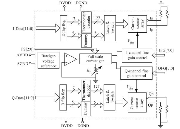
Fig. 1.
Block diagram of the proposed DAC.
SEMICONDUCTOR INTEGRATED CIRCUITS
Hualian Tang, Yiqi Zhuang, Xin Jing and Li Zhang
Corresponding author: Tang Hualian, Email:lily_thl@126.com
Abstract: This paper presents a two-channel 12-bit current-steering digital-to-analog converter (DAC) for I and Q signal paths in a wireless transmitter. The proposed DAC has a full-scale output current with an adjusting range of 2 to 10 mA. A gain matching circuit is proposed to reduce gain mismatch between the I and Q channels. The tuning range is ±24% of full scale and the minimum resolution is 1/16 LSB. To further improve its dynamic performance, the switch driver and current cell are optimized to minimize glitch energy. The chip has been processed in a standard 0.13 μm CMOS technology. Gain mismatch between a I-channel DAC and a Q-channel DAC is measured to be approximately 0.13%. At 120-MSPS sample rate for 1 MHz sinusoidal signal, the spurious free dynamic range (SFDR) is 75 dB. The total power dissipation is 62 mW and has an active area of 1.08 mm2.
Keywords: digital-to-analog converter, gain, mismatch, switch, current cell
| [1] |
Ko Y J, Stapleton S. Gain and phase mismatch effects on double image rejection transmitter. IET Circuits, Devices & Systems, 2011, 5(3):21221
|
| [2] |
Yao Xiaocheng, Gong Zheng, Shi Yin. A programmable gain amplifier with digitally assisted DC offset calibration for a direct-conversion WLAN receiver. Journal of Semiconductors, 2012, 33(11):115006 doi: 10.1088/1674-4926/33/11/115006
|
| [3] |
Yang G, Li J, Liu J. Adaptive gain and delay mismatch cancellation for LINC transmitter. Analog Integrated Circuits and Signal Processing, 2010, 65(1):151 doi: 10.1007/s10470-010-9477-5
|
| [4] |
Lin C H, Bult K. A 10-b, 500-MSample/s CMOS DAC in 0.6 mm2. IEEE J Solid-State Circuits, 1998, 33(12):1948 doi: 10.1109/4.735535
|
| [5] |
Pelgrom M J M, Duinmaijer A C J, Welbers A P G. Matching properties of MOS transistors. IEEE J Solid-State Circuits, 1989, 24(5):1433 doi: 10.1109/JSSC.1989.572629
|
| [6] |
Van den Bosch A, Steyaert M, Sansen W. An accurate statistical yield model for CMOS current-steering D/A converters. Analog Integrated Circuits and Signal Processing, 2001, 29(3):173 doi: 10.1023/A:1011261330190
|
| [7] |
Van der Plas G A M, Vandenbussche J, Sansen W, et al. A 14-bit intrinsic accuracy Q2 random walk CMOS DAC. IEEE J Solid-State Circuits, 1999, 34(12):1708 doi: 10.1109/4.808896
|
| [8] |
Kuo K C, Wu C W. A switching sequence for linear gradient error compensation in the DAC design. IEEE Trans Circuits Syst, 2011, 58(3):502 doi: 10.1007%2F978-1-4757-3724-0_3.pdf
|
| [9] |
Zhang Huajiang, Guo Gan, Li Dan, et al. A two-channel 10 bit 80 MHz CMOS current-steering D/A converter. 8th International Conference on Solid-State and Integrated Circuit Technology, 2007:1721
|
| [10] |
Analog Devices. Understanding High Speed DAC Testing and Evaluation (AN-928), 2008, www.analog.com
|
| [11] |
Gulati K, Peng M, Pulincherry A, et al. A highly integrated CMOS analog baseband transceiver with 180 MSPS 13-bit pipelined CMOS ADC and dual 12-bit DACs. IEEE J Solid-State Circuits, 2006, 41(8):1856 doi: 10.1109/JSSC.2006.875287
|
| [12] |
Seon J K, Ha S M, Yoon K S. An I/Q channel 12-bit 120 MS/s CMOS DAC with deglitch circuits. Analog Integrated Circuits and Signal Processing, 2012, 72(1):65 doi: 10.1007/s10470-012-9837-4
|
Table 1. Performance comparison of the proposed work with other works.

|
| [1] |
Ko Y J, Stapleton S. Gain and phase mismatch effects on double image rejection transmitter. IET Circuits, Devices & Systems, 2011, 5(3):21221
|
| [2] |
Yao Xiaocheng, Gong Zheng, Shi Yin. A programmable gain amplifier with digitally assisted DC offset calibration for a direct-conversion WLAN receiver. Journal of Semiconductors, 2012, 33(11):115006 doi: 10.1088/1674-4926/33/11/115006
|
| [3] |
Yang G, Li J, Liu J. Adaptive gain and delay mismatch cancellation for LINC transmitter. Analog Integrated Circuits and Signal Processing, 2010, 65(1):151 doi: 10.1007/s10470-010-9477-5
|
| [4] |
Lin C H, Bult K. A 10-b, 500-MSample/s CMOS DAC in 0.6 mm2. IEEE J Solid-State Circuits, 1998, 33(12):1948 doi: 10.1109/4.735535
|
| [5] |
Pelgrom M J M, Duinmaijer A C J, Welbers A P G. Matching properties of MOS transistors. IEEE J Solid-State Circuits, 1989, 24(5):1433 doi: 10.1109/JSSC.1989.572629
|
| [6] |
Van den Bosch A, Steyaert M, Sansen W. An accurate statistical yield model for CMOS current-steering D/A converters. Analog Integrated Circuits and Signal Processing, 2001, 29(3):173 doi: 10.1023/A:1011261330190
|
| [7] |
Van der Plas G A M, Vandenbussche J, Sansen W, et al. A 14-bit intrinsic accuracy Q2 random walk CMOS DAC. IEEE J Solid-State Circuits, 1999, 34(12):1708 doi: 10.1109/4.808896
|
| [8] |
Kuo K C, Wu C W. A switching sequence for linear gradient error compensation in the DAC design. IEEE Trans Circuits Syst, 2011, 58(3):502 doi: 10.1007%2F978-1-4757-3724-0_3.pdf
|
| [9] |
Zhang Huajiang, Guo Gan, Li Dan, et al. A two-channel 10 bit 80 MHz CMOS current-steering D/A converter. 8th International Conference on Solid-State and Integrated Circuit Technology, 2007:1721
|
| [10] |
Analog Devices. Understanding High Speed DAC Testing and Evaluation (AN-928), 2008, www.analog.com
|
| [11] |
Gulati K, Peng M, Pulincherry A, et al. A highly integrated CMOS analog baseband transceiver with 180 MSPS 13-bit pipelined CMOS ADC and dual 12-bit DACs. IEEE J Solid-State Circuits, 2006, 41(8):1856 doi: 10.1109/JSSC.2006.875287
|
| [12] |
Seon J K, Ha S M, Yoon K S. An I/Q channel 12-bit 120 MS/s CMOS DAC with deglitch circuits. Analog Integrated Circuits and Signal Processing, 2012, 72(1):65 doi: 10.1007/s10470-012-9837-4
|


Article views: 3877 Times PDF downloads: 44 Times Cited by: 0 Times
Received: 07 January 2013 Revised: Online: Published: 01 June 2013
| Citation: |
Hualian Tang, Yiqi Zhuang, Xin Jing, Li Zhang. An I/Q DAC with gain matching circuit for a wireless transmitter[J]. Journal of Semiconductors, 2013, 34(6): 065006. doi: 10.1088/1674-4926/34/6/065006
****
H L Tang, Y Q Zhuang, X Jing, L Zhang. An I/Q DAC with gain matching circuit for a wireless transmitter[J]. J. Semicond., 2013, 34(6): 065006. doi: 10.1088/1674-4926/34/6/065006.

|
| [1] |
Ko Y J, Stapleton S. Gain and phase mismatch effects on double image rejection transmitter. IET Circuits, Devices & Systems, 2011, 5(3):21221
|
| [2] |
Yao Xiaocheng, Gong Zheng, Shi Yin. A programmable gain amplifier with digitally assisted DC offset calibration for a direct-conversion WLAN receiver. Journal of Semiconductors, 2012, 33(11):115006 doi: 10.1088/1674-4926/33/11/115006
|
| [3] |
Yang G, Li J, Liu J. Adaptive gain and delay mismatch cancellation for LINC transmitter. Analog Integrated Circuits and Signal Processing, 2010, 65(1):151 doi: 10.1007/s10470-010-9477-5
|
| [4] |
Lin C H, Bult K. A 10-b, 500-MSample/s CMOS DAC in 0.6 mm2. IEEE J Solid-State Circuits, 1998, 33(12):1948 doi: 10.1109/4.735535
|
| [5] |
Pelgrom M J M, Duinmaijer A C J, Welbers A P G. Matching properties of MOS transistors. IEEE J Solid-State Circuits, 1989, 24(5):1433 doi: 10.1109/JSSC.1989.572629
|
| [6] |
Van den Bosch A, Steyaert M, Sansen W. An accurate statistical yield model for CMOS current-steering D/A converters. Analog Integrated Circuits and Signal Processing, 2001, 29(3):173 doi: 10.1023/A:1011261330190
|
| [7] |
Van der Plas G A M, Vandenbussche J, Sansen W, et al. A 14-bit intrinsic accuracy Q2 random walk CMOS DAC. IEEE J Solid-State Circuits, 1999, 34(12):1708 doi: 10.1109/4.808896
|
| [8] |
Kuo K C, Wu C W. A switching sequence for linear gradient error compensation in the DAC design. IEEE Trans Circuits Syst, 2011, 58(3):502 doi: 10.1007%2F978-1-4757-3724-0_3.pdf
|
| [9] |
Zhang Huajiang, Guo Gan, Li Dan, et al. A two-channel 10 bit 80 MHz CMOS current-steering D/A converter. 8th International Conference on Solid-State and Integrated Circuit Technology, 2007:1721
|
| [10] |
Analog Devices. Understanding High Speed DAC Testing and Evaluation (AN-928), 2008, www.analog.com
|
| [11] |
Gulati K, Peng M, Pulincherry A, et al. A highly integrated CMOS analog baseband transceiver with 180 MSPS 13-bit pipelined CMOS ADC and dual 12-bit DACs. IEEE J Solid-State Circuits, 2006, 41(8):1856 doi: 10.1109/JSSC.2006.875287
|
| [12] |
Seon J K, Ha S M, Yoon K S. An I/Q channel 12-bit 120 MS/s CMOS DAC with deglitch circuits. Analog Integrated Circuits and Signal Processing, 2012, 72(1):65 doi: 10.1007/s10470-012-9837-4
|

 WeChat ID
Journal of Semiconductors © 2017 All Rights Reserved 京ICP备05085259号-2

 DownLoad:


