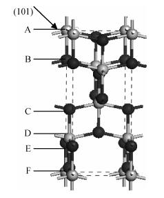
Processing math: 100%
J. Semicond. > 2013, Volume 34 > Issue 7 > 073004

SEMICONDUCTOR MATERIALS

First-principle study on the electronic and optical properties of the anatase TiO2 (101) surface

Ying Yang, Qing Feng, Weihua Wang and Yin Wang

+ Author Affiliations

 Corresponding author: Feng Qing, Email:fengq_126@163.com

DOI: 10.1088/1674-4926/34/7/073004

PDF

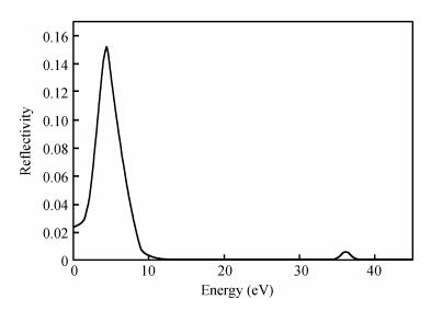
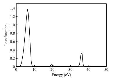
Abstract: The TiO2 (101) surface was studied using the plane-wave ultrasoft pseudopotential method based on the density functional theory, with emphasis on the structure, surface energy, band structure, density of states, and charge population. The anatase TiO2 (101) crystal surface structure, whose outermost and second layers were terminated by twofold coordinated oxygen atoms and fivefold coordinated titanium atoms, was found to be much more stable. The surface energy of the 18-layer atoms model was 0.580 J/m2. The surface electronic structure was similar to that of the bulk and no surface state. Compared with the bulk structure, the band gap increased 0.36 eV, the Ti5c-O2c bond lengths reduced 0.171 Å after relaxation, and the charges of the surface were transferred to the body. Analysis of the optical properties of the TiO2 (101) surface showed that it did not absorb in the low-energy region. An absorption edge in the ultraviolet region corresponding to the energy of 3.06 eV was found.

Key words: anataseTiO2 (101) surfacefirst-principlesdensity functional theoryelectronic structure

Self-power supply technology can solve the issues in which the battery-dependent technique suffers from its weight, size and lifetime constraints. In some special applications for security considerations, such as micro implantable medical devices, realization of self-power supply is of great significance. The key to self-power supply technique is harvesting energy from the ambient environment. More fortunately, energy in motion, heat, light, and electromagnetic radiation are inexhaustible and environmentally safe. Among these possible sources, kinetic energy in motion has a relatively high power density and scalability. Moreover, piezoelectric harvesters[1] are compatible with traditional integrated circuit technology. Its electromechanical conversion characteristics have been widely used in vibration energy harvesting (VEH). A piezoelectric harvester, vibrating at or close to its resonant frequency can be modeled as a sinusoidal current source iP in parallel with a capacitor CP and a resistor RP[24], as shown in Fig. 1. The current can be expressed as iP(t) = IP sin (2πfP t), where Ip is the amplitude of the sinusoidal current and it varies with mechanical vibration, fp is the frequency with which the piezoelectric harvester is excited. The output of a piezoelectric harvester is a sinusoidal AC signal, which needs to be converted into a DC voltage by rectifiers to supply power for micro electronic equipment. Usually, the output voltage and power of a piezoelectric harvester are low, therefore, a high-performance rectifier is required when slight vibration is excited.

Figure  1.  Equivalent circuit of a piezoelectric energy harvester.

Typical piezoelectric harvesters can provide an energy of 10–500 μW/cm2[5, 6], which is undoubtedly a serious constraint on the design of a relevant power management interface circuit. Full bridge rectifiers are widely used in commercial applications due to their simple structure and good reliability. But the large threshold voltage loss limits its further application. Meanwhile, the poor extraction capability is also one reason that limits its output power of a piezoelectric energy interface circuit. Most of the charge available from the harvester does not flow into the output at high voltage. The loss in charge due to charging and discharging of CP limits the maximum power that an interface circuit can extract. For full bridge rectifier, current iP needs to charge or discharge CP from – ( VL + 2VD) to (VL + 2VD) before it flows into the output, where VD is the voltage drop loss on a diode, as shown in Fig. 2. In order to improve the power extraction capability from piezoelectric harvesters, many efficient interface circuits[7, 8] are put forward, including maximum power point tracking (MPPT)[9, 10], synchronous charge extraction circuit (SECE)[1, 11] and synchronous switch harvesting on inductor (SSHI)[1214]. Among these interface circuits, SSHI circuits have received considerable attentions due to their high extraction efficiency and power efficiency. SSHI circuits are used to optimize the charge flipping of CP in RLC system by controlling the synchronous switches. SSHI can be classified into two categories: parallel-SSHI (P-SSHI) and series-SSHI (S-SSHI). As Refs. [6, 15] presented, performance of P-SSHI is better than that of S-SSHI, especially when vibration energy is relatively weak.

Figure  2.  Full bridge rectifier and associated waveforms.

Aiming at improving the low power conversion efficiency and poor power extraction capability of a conventional full bridge rectifier, a P-SSHI rectifier with high conversion efficiency is proposed in this paper. Active diodes instead of traditional ones are adopted to reduce voltage drop loss over the rectifying path. P-SSHI is introduced to improve the poor power extraction capability of the proposed rectifier. At the same time, LDO has a large transient output power thanks to the power management unit worked in intermittent mode. The whole energy harvesting system can achieve self-powered supply[16, 17]. This paper is organized as follows: Section 2 mainly introduces the basic principle of the P-SSHI circuit. Section 3 shows the proposed P-SSHI rectifier and IPMU. Simulation results and performance analysis are given in Section 4, followed by a summary of the article.

In order to reduce the loss in charge due to charging and discharging of CP and improve the power extraction capability of a traditional full bridge rectifier, an SO (switch-only) rectifier[13] was proposed by Ramadass et al. In Ref. [13], a power switch is connected in parallel with the piezoelectric harvester, the switch turns on for a brief time to reset CP when current iP crosses zero. Thus iP only needs to charge CP up to VL before it flows into the output during both half-cycles of the input current. Although SO rectifier can reasonably reduce the energy used to discharge CP, there are still plenty of charges used to charge CP up and wasted. P-SSHI rectifiers are successfully proposed and measured by Ramadass et al.[13] and Aktakka et al.[16]. By adopting an additional inductor of LF, P-SSHI rectifiers can greatly improve the power extraction efficiency from the piezoelectric harvester.

Basic schematic diagram and working processes of the proposed P-SSHI circuit are illustrated in Fig. 3. When Vf < Ve < VL, power switch S1 is on and D5 is off in the first branch of the P-SSHI circuit and S2 and D6 are off in the second branch. Thus there are no current flows from node e to node f through the P-SSHI circuit, and no current flows to output. Capacitor CP is charged by iP until Ve = VL. At this moment, D1 and D4 turn on and current flows to output. At time tπ, when iP crosses zero and changes direction, CP is discharged and Ve starts decreasing. D1 and D4 are then off. After that, S1 is off while S2 is on. Therefore CP, S2, D6, and LF subsequently form a resonant loop. The resonant loop, including LF and CP, helps to flip the voltage across CP. All the energy stored onCP is initially transferred to inductorLF, and then this energy is transferred back to capacitor CP where the voltage is reversed. Due to the presence of D6 in the loop, current iP flows only from e to S2, D6, and f. Thus, the flipping procedure automatically finishes after all the energy from LF is transferred back to CP without any conditional control circuits. A similar effect occurs in negative half cycle of the transducer current. This process makes full use of the obtained energy and improves the energy efficiency. The above description is of the diode D1–D6 as ideal diodes, ignoring the diode conduction drop loss of VD.

Figure  3.  Basic structure of the P-SSHI rectifier and operational waveforms.

Detecting the zero-crossing point of iP effectively has a great influence on the performance of the whole P-SSHI circuit. Taking into account commercial prospects of the entire PEH system, the complexity of the whole circuit and the self-power supply, the proposed P-SSHI circuit should detect the current changes every half cycle adaptively. The closing time of the switch should be automatically controlled to match the voltage reversal time to obtain a high flipping efficiency. In Refs. [6, 14], a reference voltage Vref which is set slightly higher than – VD of a diode is adopted, helping to detect the zero-crossing point of iP. Ideally, the LC resonant loop makes the voltage flip on CP the same absolute value. However, due to the conduction loss of inductor LF and MOS switches, the flipping voltage can only reach ±VS, which greatly affects the efficiency of the P-SSHI circuit. In addition, it is necessary to ensure that the total power consumption is less than the harvesting energy to realize the realization of self-powered supply.

Active diodes are widely used to replace traditional PN junction diodes to prevent current backflow and reduce on-resistance of the rectifying path. As shown in Fig. 4, the active diode consists of a PMOS switch and a control comparator[18]. The source terminal and drain terminal of the PMOS switch are connected to the non-inverting terminal and the inverting terminal of the comparator, respectively. The gate voltage of the MPS is controlled by VCOMP. The comparator-based active diode has the characteristics of an ideal diode. Once the voltage of node A is greater than node B, MPS turns on and turns off otherwise.

Figure  4.  Model of an active diode.

In start-up phase or output voltage of the rectifier VL is very small, the comparator cannot work normally. An auxiliary bypass PMOS diode (MPBD) in parallel to the active diode is adopted to ensure a safe stare-up of an active rectifier under different conditions. When the output voltage of the rectifier increases slowly and the comparator can operate normally, MPBD is no longer operating and always in a high impedance state. Additionally, effect of substrate leakage current cannot be ignored due to the large size of the MPBD and MPS in the active diode. The proposed bulk regulation circuit ensures the substrate potentials of MPBD and MPS are always connected to the higher of the anode voltage and the cathode voltage, preventing the substrate PN junction generates substrate leakage current.

Fig. 5 shows the basic block diagram of the interface circuit presented in this paper. Based on 0.18 μm CMOS technology, a simple and efficient P-SSHI rectifier circuit and its power management circuit are designed and verified. The output signal of the piezoelectric harvester is rectified by the full bridge rectifier. The output DC voltage is stored on capacitor CL. Active diodes instead of traditional passive ones are used thus the voltage loss over the rectifier is some tens of millivolt, which results in a power efficiency of over 90%. In P-SSHI circuit, the control circuit is designed by detecting the zero-crossing point of iP and the change of inductor current. It can adaptively and precisely control the switch on and off in the P-SSHI circuit. The IPMU with hysteresis comparators works in intermittent mode to ensure the interface circuit has a large transient output power. The output voltage of the rectifier set in the range of 2.2 to 2 V is also to prevent the MOS transistors from breakdown. With P-SSHI circuit, the output voltage range of 2.2 to 2 V may have a lower power efficiency under certain conditions. In these cases, the rectifier still has a large power output and will be analyzed in the following section. The proposed P-SSHI rectifier interface circuit can be self-powered without the need of additional power supply.

Figure  5.  Structure of the proposed interface circuit.

Fig. 6 presents a high efficiency P-SSHI rectifier circuit. It consists of an active full bridge rectifier and a P-SSHI circuit. The proposed active full bridge rectifier consists of four comparator-based active diodes. Comparators COMP1 and COMP2 adopt the same PMOS source input structure. Similarly, comparators COMP3 and COMP4 use the same NMOS source input structure. The P-SSHI circuit consists of an inductor LF, a pair of power switches MS1 and MS2, two active diodes D5 and D6 and a switch control unit.

Figure  6.  The proposed P-SSHI active rectifier.

At the start-up phase, comparators in active diodes cannot work properly. Thus, the full bridge rectifier is composed of four MPBDs. After active diodes start working, these bypass diode are always in high impedance state. When the rectifier works normally, taking the positive cycle of iP for an example, the charge of CP makes voltage VP keep rising while VN is declining. When VP is greater than VL, comparator COMP1 outputs low level, and MSP1 is on. At the same time, VN is lower than GND, comparator COMP4 outputs high level, and MSN2 is on. Thus, piezoelectric energy is transferred to capacitor CL through MSP1, CS and MSN2 and backflows to piezoelectric harvester.

When current iP gradually reduces to zero, thus VP is equal to VL, then COMP1 output is high, and MSP1 turns off, there is no rectifier path at this time. When current iP changes direction, it firstly charges VN and discharges VP. At the same time, since the non-inverting terminal voltage of COMP5 is greater than the inverting terminal voltage, COMP5 outputs high level, MN1 turns on while MN2 turns off similarly. The zero-crossing point of iP is precisely detected by comparing VP and VN with a reference voltage Vref. The reference voltage Vref is set to zero. Vref should be set to the negative value of the voltage drop across an active diode. The selected Vref will affect the current detection accuracy of iP. When VN is higher than Vref, Q2 is low level and the same as Q1. The switching logic control signals CLK1 and CLK2 can be obtained through the two signals Q1 and Q2, which reveal the zero-crossing point of iP every cycle. Then CLK1 becomes high level and MS1 turns on. Since VP is still greater than VN, MN1 remains in on state. Thus, a resonant loop circuit of CP, LF, MN1 and MS1 is generated. All of the energy stored in the capacitor CP is initially converted into the inductor. When voltage is flipped, the charge in the inductor is shared to capacitor CP finally. When VP is gradually discharged equal to zero, MN1 turns off, and the voltage flipping is completed. It is similar to that of the negative cycle of iP. The P-SSHI circuit can reduce the loss in charge due to charging and discharging of CP dramatically, resulting in a good extraction capability of the proposed rectifier.

From the structure of the circuit, NOR gate output frequency is two times the frequency of its input signal. The signal CLK1 becomes high level, while CLK2 remains low. Then MS1 turns on while MS2 is off when current iP changes its direction from positive to negative. Similarly, when iP changes from negative to positive, signal CLK1 should remain low, while signal CLK2 changes from low level to high level, thus MS2 turns on while MS1 is off. Therefore, a frequency division is needed. Fig. 7(a) is the clock divider circuit and Fig. 7(b) shows the control signals of CLK1 and CLK2.

Figure  7.  (a) Clock divider circuit (b) and its associated waves.

Taking into account the needs of an actual circuit, comparators used in this paper are shown in Fig. 8. Comparators COMP1 and COMP2 adopt the same PMOS source input structure while COMP3 and COMP4 use NMOS source input structure. All of the comparators are powered by the output of the rectifier. All transistors are biased in subthreshold region to consume less current. The specific implementation of the proposed comparators, COMP1 and COMP3, whose topologies are symmetrical are shown in Fig. 8. Taking COMP1 as an example, the comparator consists of two pairs of common gate input stages (MP1, MP2 and MP3, MP4), a current mirror (MN1, MN2), a common source inverter (MP5, MN4), and a push-pull inverter (MP6, MN5). The first stage is common-gate stage structure, which can be compatible with the input signal range of the rectifier circuit. The second stage and third stage are common-source amplifiers to provide high gain and increased output swing. The working principle is: Vin+ remains constant while Vin- increases, the current of MN2 goes up with the increase of current flowing through MP2. However, the current flowing through MP4 keeps constant, thus the gate voltage of MP4 rises up. The current flow through MP3 becomes smaller, comparator outputs low. Power switch MSP1 in Fig. 6 is on. A similar process can be shown when Vin+ is higher than Vin.

Figure  8.  Schematics of comparators used in active diodes.

Amplitude and frequency of a piezoelectric harvester change with surrounding environment, so the rectifier may not be able to provide stable supply power to the load. In order to meet the requirements of different devices for power consumption, an intermittent power management unit[16, 19] is proposed in this paper. As shown in Fig. 5, the IPMU consists of an oscillator, a hysteresis comparator, a bandgap reference and a low power output cap-less LDO.

Fig. 9(a) shows the proposed hysteresis comparator[20]. PMOS transistors, MP2 and MP3, form a latch. MP1 and MP4 are used to reset the latch. When signal S3 is low, MP1 and MP4 are on, MN5 and MN6 are off, nodes B and C are pulled up to a high level. The process is equivalent to a reset action. In the latch comparator, the input voltage VA and the reference voltage Vref1 determine the current magnitude of MN3 and MN4. When VA is greater than Vref1, current flow through MN3 is larger than that of MN4, node B is quickly pulled down to a low level while node C is pulled up to a high level by MP3, so as to achieve the function of a comparison.

When VL ranges from 2 to 2.2 V, VOUT1 remains low level while S4 is high level. Thus VL is sampled and divided by capacitors C1, C2 and C3. The gate voltage of MN1 is VA = VLC1/(C1 + C2 + C3). When VL is equal to 2.2 V, VOUT1 becomes high level while S4 becomes low. Then VL begins to decrease due to the load consumption. When VL ranges from 2.2 to 2 V, signal S4 remains unchanged. Thus VA = VLC1/(C1 + C2). When VL decreases to 2 V, S4 becomes high level again. We adjust the ratio of C1C3 to set VL between 2.2 and 2.0 V. The control signals of the comparator are shown in Fig. 9(b). When S1 is high while S2 and S3 are low, VL is sampled and stored on C1 and comparator is reset. When S1 is low, the voltage stored on C1 is divided by C2 and C3. After the completion of the share process, S2 becomes high level and the comparator starts to work. When the output of the comparator is set by comparing VA with Vref1, a sample signal S3 arrives and VOUT1 follows with the change of the output signal. The switching frequency of S1 is set to 100 kHz, which is much higher than the frequency of the piezoelectric harvester. Thus the sampling of signal VL can be treated as continuous. The use of switched-capacitor voltage divider not only reduces the power consumption of the comparator, but also the area of the layout.

Figure  9.  Schematic of (a) the hysteresis comparator and (b) its control signals.

In order to meet the requirements of ultra-micro energy harvesting as well as the power consumption, a bandgap reference circuit[21, 22] was introduced in IPMU, as shown in Fig. 10.

Figure  10.  Schematic of the proposed bandgap reference circuit.

The reference consists of a start-up circuit, a bias circuit and a bandgap reference core circuit. The design of the start-up circuit can quickly generate a bias current to solve the degenerate operating point in the reference circuit. Once the core circuit reaches a stable state, the start-up circuit turns off automatically. In the reference core, the cascade amplifier senses VA and VB such that node A and B settle to approximately equal voltages. The reference voltage is obtained at the source terminal of Mnative. Hence a reference voltage of

Vref1=VBE2+VT(lnn)R3[R2+R3+2(R4+R5+Rtrim)].
(1)

With a PTAT (proportional to absolute temperature) voltage and a CTAT (complementary to absolute temperature) voltage, a temperature independent bandgap reference can be obtained. Moreover, for better TC and more accuracy, trimming resistors R6, R7 and R8 are utilized.

Due to the low accuracy and large ripple of the output voltage of the proposed rectifier, a low dropout linear regulator (LDO) is designed to obtain a high precision and low ripple DC voltage. Traditional LDOs need a large off-chip filter capacitor to achieve a very small output voltage ripple and ensure the stability of the system. But it is not conducive to integration. Therefore, to perfect the harvesting system, an output cap-less LDO[23, 24] is adopted as a power management circuit to regulate the output of the rectifier, the simplified structure is shown in Fig. 11. The proposed LDO reduces the filter capacitor size dramatically, and it can also be integrated.

Figure  11.  Structure of the proposed cap-less LDO.

The proposed design, which consists of a P-SSHI active rectifier and an IPMU, has been designed, implemented and simulated in a 0.18 μm CMOS process. The corresponding open-circuit voltage amplitude of the piezoelectric harvester was 2.0 V for this simulation. The working frequency is 225 Hz for a commercial use. The simulated power consumptions of the proposed interface circuit are analyzed firstly. Then simulation results of the P-SSHI active rectifier are given and followed by the function of the IPMU.

The design consists of an active full-bridge, a P-SSHI circuit and an IMPU. The following power consumption is measured at the output VL of 2 V. The active full-bridge rectifier consists of four active diodes AD1–AD4, each active diode dissipates a bias current of 200 nA, and the power loss is 1.6 μW. The P-SSHI consists of four comparators COMP5– COMP8. COMP5 and COMP6 consume a very small current since they have no requirement on performance. To assure a high detecting resolution and speed, COMP7 and COMP8 need a large current. But they are only needed to work when iP reduces to zero-crossing point, so its average current over the entire period is also small. The average current consumption of the P-SSHI is 175 nA, and the power loss is 0.35 μW. The IMPU consists of an oscillator CLK, a hysteresis comparator HC, a voltage bandgap reference BGR and a LDO. The BGR consumes a current of 0.4 μA. The total current loss of the IMPU is 0.8 μA. The simulated current consumptions of the stages are listed in Table 1.

Table  1.  Overall power consumption of the interface circuit.
Stage Value (μW)
P-SSHI COMP5–COMP8 0.35
Active-full bridge AD1–AD4 1.6
IMPU CLK, HC, BGR, LDO 1.6
Total power loss 3.55
DownLoad: CSV  | Show Table

The performance of the rectifier has a great influence on the function and efficiency of the whole energy harvesting system. The simulated voltage waves across CP of the proposed P-SSHI rectifier with an 820 μH inductor is shown in Fig. 12.

Figure  12.  (Color online) Flipping efficiency of the proposed P-SSHI rectifier.

As the wave shows, voltage VF across CP is naturally inverted, the flipping efficiency of the circuit is given as Eq. (2)

ηF=VF+VL2VL×100%.
(2)

From the Eq. (2) and the simulation results, we can easily obtain the flipping efficiency of over 80%. The current detecting accuracy of iP is less than 6 μA, very close to the zero-crossing point of IP. The maximum output power that the full-bridge rectifier can obtain is given by Eq. (3)

PREC(max)=CP(VP2VD)2fP,
(3)

where VP = IP/ωPCP. This is achieved at VL = VP/2 – VD. From Eq. (3), the drop loss VD has a great influence on the output power of the rectifier.

Fig. 13 is output power comparison between the proposed rectifier and a traditional one. As the figure shows, for a traditional full bridge with VD = 0.4 V, the maximum output power is 5.8 μW at VL of 0.6 V. The maximum output power is 13.3 μW and VL of 0.94 V the proposed active full-bridge rectifier can obtain. Thanks to the active diodes reducing the voltage drop loss on the rectifying path, the maximum output power of the proposed active full-bridge rectifier is 2.3 × that of a traditional one. In addition, a traditional full-bridge with P-SSHI achieves an output power of 34.24 μW at VL of 2 V. The proposed active P-SSHI rectifier can achieve an output power of 44.4 μW at VL of 2 V, the increase is 30% compared to a traditional P-SSHI rectifier. Even though the effect of P-SSHI cannot be fully released, the output power of the proposed P-SSHI rectifier at VL of 2.0 V is much greater than the maximum output power that an active rectifier or a traditional one with P-SSHI can obtain. Both active diodes and P-SSHI help to improve the output power of the proposed rectifier.

Figure  13.  (Color online) Simulated output power of the proposed P-SSHI rectifier.

The simulation results of reference voltage versus temperature are shown in Fig. 14(a), which shows the TC (temperature coefficient ) of the reference voltage is 25.98 ppm/°C when the swept temperature is ranging from −45 to 85 °C. Fig. 14(b) is the 200 Monte Carlo simulation results of the bandgap reference on its offset voltage with process and mismatch variations. It can be seen from the histogram that the mean value (μ) of the reference voltage is 1.19239 V with the standard deviation (σ) of 3.96 mV. The coefficient of variation for it is about 0.33%.

Figure  14.  (Color online) (a) Reference voltage versus temperature. (b) 200 Monte Carlo simulation results.

Simulated results of the proposed IPMU are shown in Fig. 15. The output voltage VL of the proposed P-SSHI rectifier changes relatively slowly when a small input voltage instead of a large one is considered. When VL rises up to 2.2 V, LDO is used as a followed load stage to consume power and provide a stable and precise output voltage of 1.8 V. Then VL begins to decline, when VL drops to 2.0 V, LDO stops working. As the simulation waveform shows, VL vibrates between 2.2–2.0 V regularly. The power management unit works in intermittent mode can provide a large transient output power for LDO to meet different devices for different power demand.

Figure  15.  (Color online) Simulated function of the proposed IPMU.

Fig. 16 shows the loop stability of the LDO with different load conditions. When the Iload is 1 μA, the phase margin of the loop is 60°. When load current increases to 1 mA, the phase margin of the loop is 80°. The gain bandwidth product of the loop is 500 kHz. The proposed cap-less LDO can ensure the loop stable with different load conditions.

Figure  16.  (Color online) Loop stability of the LDO with different loads.

Fig. 17 shows the overall layout of the piezoelectric energy harvesting system. The chip area of is 1.1 × 1.1 mm2, and the core area of the rectifier is 0.31 × 0.39 mm2. All power switches are isolated from the adjacent circuits by the protection rings. The parasitic parameters of the P-SSHI rectifier have been extracted and process corner models have been considered to obtain more accurate simulation results.

Figure  17.  (Color online) (a) Layout of the chip. (b) Layout of the core.

A comparison with other reported P-SSHI rectifiers is summarized in Table 2. The FOM is defined as the ratio of the maximum output power of the proposed rectifier and that of the traditional full-bridge rectifier. From the table, only the proposed P-SSHI rectifier and Ref. [13] show a CMOS integration and performance enhanced at the same time. In Ref. [13], the maximum output power the introduced rectifier with an 820 μH inductor can obtain is 47 μW, which is 4× greater than that of the full bridge. An interface circuit with good performance and load independent has been proposed in Ref. [17]. However, it is based on discrete devices and not good for the system integration. Moreover, when the open-circuit voltage of the piezoelectric transducer is less than 10 V, its conversion efficiency will be very low. So it is not applicable to low voltage and low power devices. In Ref. [27], a flipping efficiency as high as 94% is obtained, however, some external devices are needed to adjust the flip timing. The output power of the proposed P-SSHI rectifier with an 820μH inductor is 44.4 μW at VL of 2.0 V. Taking the conventional full-bridge rectifier as a common reference, the proposed rectifier can improve the harvested energy by up to 7.7× compared to the conventional full-bridge rectifier.

Table  2.  Performance comparison of the reported designs.
Parameter Process IP (μA) CP (nF) fP (Hz) ηF PO (μW) FOM: PO/PFB
Ref. [13] 0.35 μm CMOS 63 12 225 75% (LF = 820 μH) 47 4 ×
Ref. [14] Discrete 63 18 225 —(LF = 940 μH) 48 5.8 ×
Ref. [17] Discrete 1000 220 50 > 80% (LF = 1 mH) 3 ×
Ref. [25] CMOS 80 26 200 70% (LF = 400 μH) 71 4.5 ×
Ref. [26] Discrete 80 12 200 68% (LF = 22 μH) 120 3.6 ×
Ref. [27] 0.35 μm CMOS 14 9 229 94% (LF = 3.3 mH) 8.19 4.4 ×
This work 0.18 μm CMOS 50 17.5 225 > 80% (LF = 820 μH) 44.4 7.7 ×
DownLoad: CSV  | Show Table

A power-enhanced P-SSHI active full-bridge rectifier for piezoelectric energy harvesting has been designed, fabricated in SMIC 0.18 μm standard CMOS technology and simulated. The active diodes instead of traditional PN junction diodes are utilized in the rectifier, the voltage drop loss on the rectifying path is only tens of millivolts, and thus a higher power conversion efficiency is obtained. The maximum output power of the proposed active rectifier is 2.3× that of a traditional rectifier. A P-SSHI circuit is also adopted to improve the poor power extraction capability of the rectifier. The proposed P-SSHI circuit can detect the zero-crossing point of current iP precisely. The flipping efficiency of the proposed P-SSHI circuit is superior to 80%. The proposed P-SSHI rectifier can improve the harvested energy by up to 30% compared to a traditional rectifier with P-SSHI. The IPMU ensures a large transient power for the followed circuit LDO. A stable and precise voltage of 1.8 V is obtained at the output of the cap-less LDO. The proposed P-SSHI rectifier can be self-powered without any additional power supply. The size of the layout is 1.1 × 1.1 mm2.


[1]
Tao Q, Wang J. Application of TiO2 photocatalytic oxidation technology to gas-phase contaminants degradation. Safety and Environmental Engineering, 2010, 17(5):26
[2]
Hebenstreit W, Ruzycki N, Herman G S, et al. Scanning tunneling microscopy investigation of the TiO2 anatase (101) surfaces. Phys Rev B, 2000, 62:16334 doi: 10.1103/PhysRevB.62.R16334
[3]
Hengerer R, Bolliger B, Erbudak M, et al. Structure and stability of the anatase TiO2 (101) and (001) surfaces. Surf Sci, 2000, 460:162 doi: 10.1016/S0039-6028(00)00527-6
[4]
Ma Xinguo, Tang Chaoqun, Huang Jinqiu, et al. First-principle calculations on the geometry and relaxation structure of anatase TiO2 (101) surface. Acta Physica Sinica, 2006, 55(8):4208
[5]
Ma Xinguo, Jiang Jianjun, Liang Pei. Theoretical study of native point defects on anatase TiO2 (101) surface. Acta Physica Sinica, 2008, 57:3120
[6]
Finazzi E, Valentin C D, Pacchioni A S G. First principles study of nitrogen doping at the anatase TiO2 (101) surface. Phys Chem C, 2007, 111(26):9275 doi: 10.1021/jp071186s
[7]
Chen Qili, Tang Chaoqun. First-principles calculations on electronic structures of N/F-doped and N-F-codoped TiO2 anatase (101) surfaces. Acta Physico-Chimica Sinica, 2009, 25(5):915
[8]
Chen Q, Tang C, Zheng G. First-principles study of TiO2 anatase (101) surfaces doped with N. Phys B, 2009, 404:1074 doi: 10.1016/j.physb.2008.11.032
[9]
Kresse G, Joubert D. From ultrasoft pseudopotentials to the projector augmented-wave method. Phys Rev B, 1999, 59:1758
[10]
Zhao Zongyan, Liu Qingju, Zhu Zhongqi, et al. First-principles calculation of electronic structure and optical properties of anatase TiO2. Chinese Journal of Semiconductors, 2007, 28(10):1555
[11]
Perdew J P, Chevary J A, Vosko S H, et al. Atoms, molecules, solids, and surfaces:applications of the generalized gradient approximation for exchange and correlation. Phys Rev B, 1992, 46:6671 doi: 10.1103/PhysRevB.46.6671
[12]
Perdew J P, Wang Y. Accurate and simple analytic representation of the electron-gas correlation energy. Phys Rev B, 1992, 45:13244 doi: 10.1103/PhysRevB.45.13244
[13]
Hammer B, Hansen L B, Norskov J K. Improved adsorption energetics within density-functional theory using revised Perdew-Burke-Ernzerhof functional. Phys Rev B, 1999, 59:7413 doi: 10.1103/PhysRevB.59.7413
[14]
Wu Z, Cohen R E. A more accurate generalized gradient approximation for solids. Phys Rev B, 2006, 73:235116 doi: 10.1103/PhysRevB.73.235116
[15]
Perdew J P, Ruzsinszky A, Csonka G, et al. Restoring the density-gradient expansion for exchange in solids and surfaces. Phys Rev Lett, 2008, 100:136406 doi: 10.1103/PhysRevLett.100.136406
[16]
Ceperley D M, Alder B J. Ground state of the electron gas by a stochastic method. Phys Rev Lett, 1980, 45:566 doi: 10.1103/PhysRevLett.45.566
[17]
Diebold U. The surface science of titanium dioxide. Surf Sci Rep, 2003, 48:53 doi: 10.1016/S0167-5729(02)00100-0
[18]
Segall M D, Lindan P L D, Probert M J, et al. First-principles simulation:ideas, illustrations and the CASTEP code. Journal of Physics:Condensed Matter, 2002, 14:2717 doi: 10.1088/0953-8984/14/11/301
Fig. 1.  Direction of the different shear positions of the anatase TiO2 (101)

Fig. 2.  Atomic structure of the anatase TiO2 (101) surface (a) before and (b) after optimization

Fig. 3.  Band structure and state density of anatase TiO2 (101) surface and bulk. (a) Band structure of bulk anatase TiO2. (b) State density of bulk anatase TiO2. (c) Band structure of the anatase TiO2 (101) surface. (d) State density of the anatase TiO2 (101) surface

Fig. 4.  Real and imaginary parts of the curve of the dielectric function versus the photon energy change on the anatase TiO2 (101) surface

Fig. 5.  Optical absorption curves of the anatase TiO2 (101) surface

Fig. 6.  Reflection spectrum of the anatase TiO2 (101) surface

Fig. 7.  Energy loss spectrum of the anatase TiO2 (101) surface

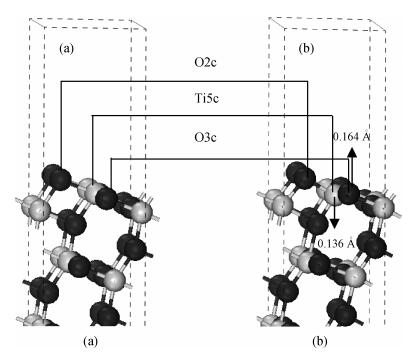
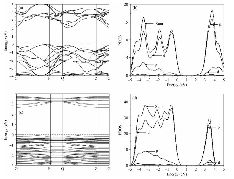
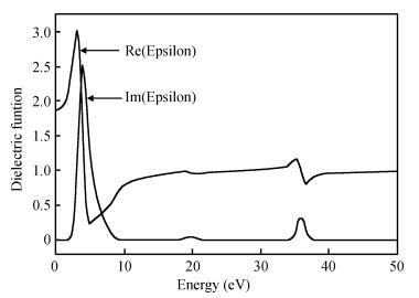
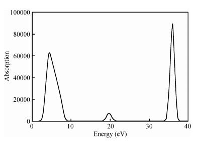
Table 1.   Experimental and theoretical values of anatase TiO2 crystal parameters

Table 2.   Total energy of different atomic termination structures with same atomic number

Table 3.   Bond lengths and population of anatase TiO2 (101) surface before and after optimization

Table 4.   Charge distribution of anatase TiO2 (101) surface

[1]
Tao Q, Wang J. Application of TiO2 photocatalytic oxidation technology to gas-phase contaminants degradation. Safety and Environmental Engineering, 2010, 17(5):26
[2]
Hebenstreit W, Ruzycki N, Herman G S, et al. Scanning tunneling microscopy investigation of the TiO2 anatase (101) surfaces. Phys Rev B, 2000, 62:16334 doi: 10.1103/PhysRevB.62.R16334
[3]
Hengerer R, Bolliger B, Erbudak M, et al. Structure and stability of the anatase TiO2 (101) and (001) surfaces. Surf Sci, 2000, 460:162 doi: 10.1016/S0039-6028(00)00527-6
[4]
Ma Xinguo, Tang Chaoqun, Huang Jinqiu, et al. First-principle calculations on the geometry and relaxation structure of anatase TiO2 (101) surface. Acta Physica Sinica, 2006, 55(8):4208
[5]
Ma Xinguo, Jiang Jianjun, Liang Pei. Theoretical study of native point defects on anatase TiO2 (101) surface. Acta Physica Sinica, 2008, 57:3120
[6]
Finazzi E, Valentin C D, Pacchioni A S G. First principles study of nitrogen doping at the anatase TiO2 (101) surface. Phys Chem C, 2007, 111(26):9275 doi: 10.1021/jp071186s
[7]
Chen Qili, Tang Chaoqun. First-principles calculations on electronic structures of N/F-doped and N-F-codoped TiO2 anatase (101) surfaces. Acta Physico-Chimica Sinica, 2009, 25(5):915
[8]
Chen Q, Tang C, Zheng G. First-principles study of TiO2 anatase (101) surfaces doped with N. Phys B, 2009, 404:1074 doi: 10.1016/j.physb.2008.11.032
[9]
Kresse G, Joubert D. From ultrasoft pseudopotentials to the projector augmented-wave method. Phys Rev B, 1999, 59:1758
[10]
Zhao Zongyan, Liu Qingju, Zhu Zhongqi, et al. First-principles calculation of electronic structure and optical properties of anatase TiO2. Chinese Journal of Semiconductors, 2007, 28(10):1555
[11]
Perdew J P, Chevary J A, Vosko S H, et al. Atoms, molecules, solids, and surfaces:applications of the generalized gradient approximation for exchange and correlation. Phys Rev B, 1992, 46:6671 doi: 10.1103/PhysRevB.46.6671
[12]
Perdew J P, Wang Y. Accurate and simple analytic representation of the electron-gas correlation energy. Phys Rev B, 1992, 45:13244 doi: 10.1103/PhysRevB.45.13244
[13]
Hammer B, Hansen L B, Norskov J K. Improved adsorption energetics within density-functional theory using revised Perdew-Burke-Ernzerhof functional. Phys Rev B, 1999, 59:7413 doi: 10.1103/PhysRevB.59.7413
[14]
Wu Z, Cohen R E. A more accurate generalized gradient approximation for solids. Phys Rev B, 2006, 73:235116 doi: 10.1103/PhysRevB.73.235116
[15]
Perdew J P, Ruzsinszky A, Csonka G, et al. Restoring the density-gradient expansion for exchange in solids and surfaces. Phys Rev Lett, 2008, 100:136406 doi: 10.1103/PhysRevLett.100.136406
[16]
Ceperley D M, Alder B J. Ground state of the electron gas by a stochastic method. Phys Rev Lett, 1980, 45:566 doi: 10.1103/PhysRevLett.45.566
[17]
Diebold U. The surface science of titanium dioxide. Surf Sci Rep, 2003, 48:53 doi: 10.1016/S0167-5729(02)00100-0
[18]
Segall M D, Lindan P L D, Probert M J, et al. First-principles simulation:ideas, illustrations and the CASTEP code. Journal of Physics:Condensed Matter, 2002, 14:2717 doi: 10.1088/0953-8984/14/11/301
1

Effect of warpage on the electronic structure and optical properties of bilayer germanene

Qihang Xiong, Weifu Cen, Xingtong Wu, Cong Chen

Journal of Semiconductors, 2022, 43(12): 122102. doi: 10.1088/1674-4926/43/12/122102

2

The electronic and magnetic properties of wurtzite Mn:CdS, Cr:CdS and Mn:Cr:CdS: first principles calculations

Azeem Nabi, Zarmeena Akhtar, Tahir Iqbal, Atif Ali, Arshad Javid, et al.

Journal of Semiconductors, 2017, 38(7): 073001. doi: 10.1088/1674-4926/38/7/073001

3

Electronic structure and optical property of p-type Zn-doped SnO2 with Sn vacancy

Guipeng Sun, Jinliang Yan, Peijiang Niu, Delan Meng

Journal of Semiconductors, 2016, 37(2): 023005. doi: 10.1088/1674-4926/37/2/023005

4

Electronic structure and optical properties of F-doped β-Ga2O3 from first principles calculations

Jinliang Yan, Chong Qu

Journal of Semiconductors, 2016, 37(4): 042002. doi: 10.1088/1674-4926/37/4/042002

5

Electronic, optical, and mechanical properties of Cu2ZnSnS4 with four crystal structures

Zongyan Zhao, Xiang Zhao

Journal of Semiconductors, 2015, 36(8): 083004. doi: 10.1088/1674-4926/36/8/083004

6

Electronic structures and phase transition characters of β-, P61-, P62- and δ-Si3N4 under extreme conditions: a density functional theory study

Dong Chen, Yuping Cang, Yongsong Luo

Journal of Semiconductors, 2015, 36(2): 023003. doi: 10.1088/1674-4926/36/2/023003

7

Effect of N and Fe codoping on the electronic structure and optical properties of TiO2 from first-principles study

Zhuomao Zhu, Baoan Bian, Haifeng Shi

Journal of Semiconductors, 2015, 36(10): 102003. doi: 10.1088/1674-4926/36/10/102003

8

First-principles calculations of Mg2X (X = Si, Ge, Sn) semiconductors with the calcium fluorite structure

Sandong Guo

Journal of Semiconductors, 2015, 36(5): 053002. doi: 10.1088/1674-4926/36/5/053002

9

In situ TEM/SEM electronic/mechanical characterization of nano material with MEMS chip

Yuelin Wang, Tie Li, Xiao Zhang, Hongjiang Zeng, Qinhua Jin, et al.

Journal of Semiconductors, 2014, 35(8): 081001. doi: 10.1088/1674-4926/35/8/081001

10

First-principles study on the synergistic effects of codoped anatase TiO2 photocatalysts codoped with N/V or C/Cr

Wenhui Xu, Xinguo Ma, Tong Wu, Zhiqi He, Huihu Wang, et al.

Journal of Semiconductors, 2014, 35(10): 102002. doi: 10.1088/1674-4926/35/10/102002

11

AC-electronic and dielectric properties of semiconducting phthalocyanine compounds:a comparative study

Safa'a M. Hraibat, Rushdi M-L. Kitaneh, Mohammad M. Abu-Samreh, Abdelkarim M. Saleh

Journal of Semiconductors, 2013, 34(11): 112001. doi: 10.1088/1674-4926/34/11/112001

12

First-principles calculation on the concentration of intrinsic defects in 4H-SiC

Ping Cheng, Yuming Zhang, Yimen Zhang

Journal of Semiconductors, 2013, 34(1): 013002. doi: 10.1088/1674-4926/34/1/013002

13

First principle study of the electronic structure of hafnium-doped anatase TiO2

Li Lezhong, Yang Weiqing, Ding Yingchun, Zhu Xinghua

Journal of Semiconductors, 2012, 33(1): 012002. doi: 10.1088/1674-4926/33/1/012002

14

First-principles study of the electronic structures and optical properties of C–F–Be doped wurtzite ZnO

Zuo Chunying, Wen Jing, Zhong Cheng

Journal of Semiconductors, 2012, 33(7): 072001. doi: 10.1088/1674-4926/33/7/072001

15

First-principle study on anatase TiO2 codoped with nitrogen and ytterbium

Gao Pan, Zhang Xuejun, Zhou Wenfang, Wu Jing, Liu Qingju, et al.

Journal of Semiconductors, 2010, 31(3): 032001. doi: 10.1088/1674-4926/31/3/032001

16

First-principles of wurtzite ZnO (0001) and (000ī) surface structures

Zhang Yufei, Guo Zhiyou, Gao Xiaoqi, Cao Dongxing, Dai Yunxiao, et al.

Journal of Semiconductors, 2010, 31(8): 082001. doi: 10.1088/1674-4926/31/8/082001

17

First principles study of the Be–C co-doped MgB2 system

Su Xiyu, Zhi Xiaofen, Hou Qinying, Cheng Wei, Liu Jiaxue, et al.

Journal of Semiconductors, 2009, 30(11): 112001. doi: 10.1088/1674-4926/30/11/112001

18

First Principle Calculation of the Electronic Structure and Optical Properties of Impurity-Doped β-FeSi2 Semiconductors

Yan Wanjun, Xie Quan

Journal of Semiconductors, 2008, 29(6): 1141-1146.

19

First-Principles Calculation of Electronic Structure and Optical Properties of Anatase TiO2

Zhao Zongyan, Liu Qingju, Zhu Zhongqi, Zhang Jin

Chinese Journal of Semiconductors , 2007, 28(10): 1555-1561.

20

Electronic Structure of Semiconductor Nanocrystals

Li Jingbo, Wang Linwang, Wei Suhuai

Chinese Journal of Semiconductors , 2006, 27(2): 191-196.

  • Search

    Advanced Search >>

    GET CITATION

    Lianxi Liu, Yanbo Pang, Wenzhi Yuan, Zhangming Zhu, Yintang Yang. A self-powered piezoelectric energy harvesting interface circuit with efficiency-enhanced P-SSHI rectifier[J]. Journal of Semiconductors, 2018, 39(4): 045002. doi: 10.1088/1674-4926/39/4/045002
    L X Liu, Y B Pang, W Z Yuan, Z M Zhu, Y T Yang. A self-powered piezoelectric energy harvesting interface circuit with efficiency-enhanced P-SSHI rectifier[J]. J. Semicond., 2018, 39(4): 045002. doi: 10.1088/1674-4926/39/4/045002.
    shu

    Export: BibTex EndNote

    Article Metrics

    Article views: 2907 Times PDF downloads: 41 Times Cited by: 0 Times

    History

    Received: 29 October 2012 Revised: 19 February 2013 Online: Published: 01 July 2013

    Catalog

      Email This Article

      User name:
      Email:*请输入正确邮箱
      Code:*验证码错误
      Lianxi Liu, Yanbo Pang, Wenzhi Yuan, Zhangming Zhu, Yintang Yang. A self-powered piezoelectric energy harvesting interface circuit with efficiency-enhanced P-SSHI rectifier[J]. Journal of Semiconductors, 2018, 39(4): 045002. doi: 10.1088/1674-4926/39/4/045002 ****L X Liu, Y B Pang, W Z Yuan, Z M Zhu, Y T Yang. A self-powered piezoelectric energy harvesting interface circuit with efficiency-enhanced P-SSHI rectifier[J]. J. Semicond., 2018, 39(4): 045002. doi: 10.1088/1674-4926/39/4/045002.
      Citation:
      Ying Yang, Qing Feng, Weihua Wang, Yin Wang. First-principle study on the electronic and optical properties of the anatase TiO2 (101) surface[J]. Journal of Semiconductors, 2013, 34(7): 073004. doi: 10.1088/1674-4926/34/7/073004 ****
      Y Yang, Q Feng, W H Wang, Y Wang. First-principle study on the electronic and optical properties of the anatase TiO2 (101) surface[J]. J. Semicond., 2013, 34(7): 073004. doi: 10.1088/1674-4926/34/7/073004.

      First-principle study on the electronic and optical properties of the anatase TiO2 (101) surface

      DOI: 10.1088/1674-4926/34/7/073004
      Funds:

      the National Natural Science Foundation of China 61106129

      the National Natural Science Foundation of China 61274128

      Project supported by the National Natural Science Foundation of China (Nos. 61106129, 61274128)

      More Information
      • Corresponding author: Feng Qing, Email:fengq_126@163.com
      • Received Date: 2012-10-29
      • Revised Date: 2013-02-19
      • Published Date: 2013-07-01

      Catalog

        /

        DownLoad:  Full-Size Img  PowerPoint
        Return
        Return