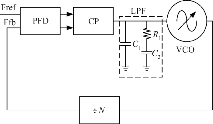
Fig. 1.
Block diagram of a typical frequency synthesizer.
SEMICONDUCTOR INTEGRATED CIRCUITS
Wenrui Zhu1, 2, Haigang Yang1, , Tongqiang Gao1 and Hui Zhang1
Corresponding author: Yang Haigang, Email:yanghg@mail.ie.ac.cn
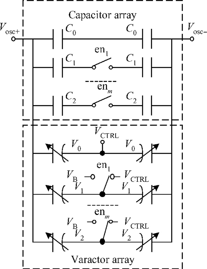
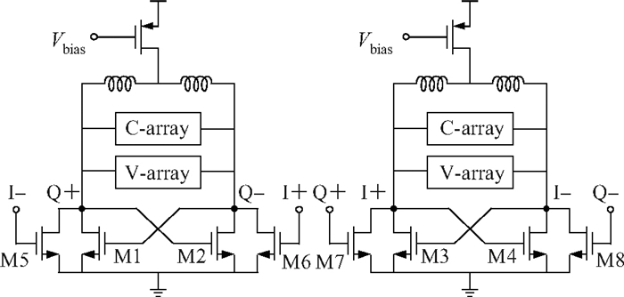
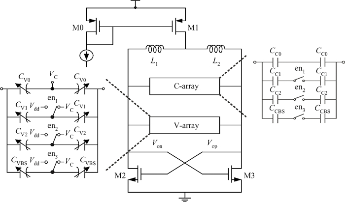
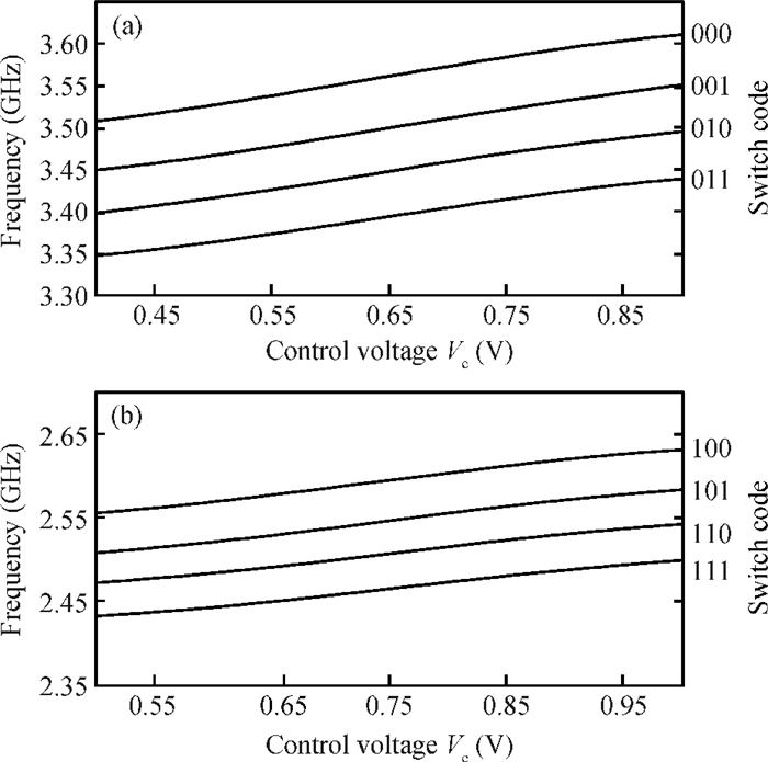
Abstract: This paper presents a novel dual-band quadrature voltage controlled oscillator (VCO) with the gain proportional to the oscillation frequency. Frequency synthesizers with this VCO can reduce the bandwidth fluctuation over all the frequency ranges without compensation or calibration. Besides the original switched capacitor array, an extra switched varactor array is adopted for the implementation of the proposed VCO. The tuning technique of changing the values of the capacitor and varactor at the same ratio is also derived. For verification purposes, a 2.5 G/3.5 G dual-band quadrature VCO is fabricated in a 0.13 μm CMOS process for WiMAX applications. Measurement results show that the VCO gain is closely proportional to the oscillation frequency with ±16% variation over the entire frequency range. The phase noise is -138.15 dBc/Hz at 10 MHz from the 2.5 GHz carrier and -137.44 dBc/Hz at 10 MHz from the 3.5 GHz carrier.
Keywords: VCO, dual-band, tuning technique, constant bandwidth
| [1] |
Lu T Y, Chen W Z. A 3-10 GHz, 14 bands CMOS frequency synthesizer with spurs reduction for MB-OFDM UWB system. IEEE Tran Very Large Scale Integration (VLSI) Syst, 2012, 20:948 doi: 10.1109/TVLSI.2011.2134874
|
| [2] |
Catli B, Hella M M. A 1.94 to 2.55 GHz, 3.6 to 4.77 GHz tunable CMOS VCO based on double-tuned, double-driven coupled resonators. IEEE J Solid-State Circuits, 2009, 44:2463 doi: 10.1109/JSSC.2009.2023155
|
| [3] |
Park E C, Hauspie D, Craninckx J. Wideband VCO with simultaneous switching of frequency band, active core, and varactor size. IEEE J Solid-State Circuits, 2007, 42:1472 doi: 10.1109/JSSC.2007.899105
|
| [4] |
Xiao Shimao, Ma Chengyan, Ye Tianchun. A novel 2.95-3.65 GHz CMOS LC-VCO using tuning curve compensation. Journal of Semiconductors, 2009, 30(10):105001 doi: 10.1088/1674-4926/30/10/105001
|
| [5] |
Li Bin, Fan Xiangning, Wang Zhigong. A wideband LC-VCO with small VCO gain variation and adaptive power control. Journal of Semiconductors, 2012, 33(10):105008 doi: 10.1088/1674-4926/33/10/105008
|
| [6] |
Lu L, Chen J, Yuan L, et al. An 18-mW 1.175-2-GHz frequency synthesizer with constant bandwidth for DVB-T tuners. IEEE Trans Microw Theory Tech, 2009, 57(4):928 doi: 10.1109/TMTT.2009.2014449
|
| [7] |
Hauspie D, Park E C, Craninckx J. Wideband VCO with simultaneous switching of frequency band, active core, and varactor size. IEEE J Solid-State Circuits, 2007, 42:1472 doi: 10.1109/JSSC.2007.899105
|
| [8] |
Zhang H. Research into design techniques of reconfigurable phase-locked loop based on standard CMOS technology. Doctor Thesis, Institute of Electronics, Chinese Academic of Sciences, 2011(in Chinese)
|
| [9] |
Akamine Y, Kawabe M, Hori K, et al. Delta-sigma PLL transmitter with a loop-bandwidth calibration system. IEEE J Solid-State Circuits, 2008, 43:497 doi: 10.1109/JSSC.2007.914325
|
| [10] |
Rao A, Mansour M, Singh G, et al. A 4-6.4 GHz LC PLL with adaptive bandwidth control for a forwarded clock link. IEEE J Solid-State Circuits, 2008, 43:2099 doi: 10.1109/JSSC.2008.2001870
|
| [11] |
Shanan H, Retz G, Mulvaney K, et al. A 2.4 GHz 2 Mb/s versatile PLL-based transmitter using digital pre-emphasis and auto calibration in 0.18μm CMOS for WPAN. IEEE International Solid-State Circuits Conference, Digest of Technical Papers, 2009:420
|
| [12] |
Shin J, Shin H. A 1.9-3.8 GHz delta-sigma fractional-N PLL frequency synthesizer with fast auto-calibration of loop bandwidth and VCO frequency. IEEE J Solid-State Circuits, 2012, 47:665 doi: 10.1109/JSSC.2011.2179733
|
| [13] |
Wu T, Hanumolu P K, Mayaram K, et al. Method for a constant loop bandwidth in LC-VCO PLL frequency synthesizers. IEEE J Solid-State Circuits, 2009, 44:427 doi: 10.1109/JSSC.2008.2010792
|
| [14] |
Feng Y, Chen G. A fractional-N synthesizer for multi-mode positioning system with constant loop bandwidth. International Conference of Electron Devices and Solid-State Circuits (EDSSC), 2011:1 http://ieeexplore.ieee.org/document/6117626/?reload=true&arnumber=6117626&filter%3DAND%28p_IS_Number%3A6117556%29
|
| [15] |
Lu L, Gong Z, Liao Y, et al. A 975-to-1960 MHz fast-locking fractional-N synthesizer with adaptive bandwidth control and 4/4.5 prescaler for digital TV tuners. IEEE International Solid-State Circuits Conference, Digest of Technical Papers, 2009:96, 397a
|
| [16] |
Zhou Chunyuan, Zhang Lei, Qian He. A uniform phase noise QVCO with a feedback current source. Journal of Semiconductors, 2012, 33(7):075001 doi: 10.1088/1674-4926/33/7/075001
|
| [17] |
Long Qiang, Zhuang Yiqi, Yin Yue, et al. Design of a CMOS multi-mode GNSS receiver VCO. Journal of Semiconductors, 2012, 33(5):055003 doi: 10.1088/1674-4926/33/5/055003
|
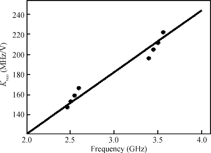
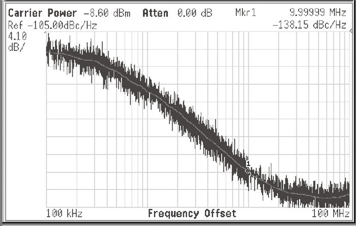
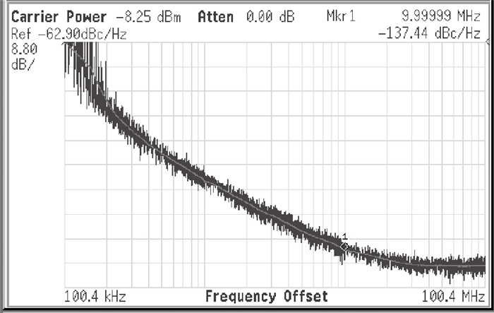
Table 1. Comparison of the proposed VCO with previous works.

|
| [1] |
Lu T Y, Chen W Z. A 3-10 GHz, 14 bands CMOS frequency synthesizer with spurs reduction for MB-OFDM UWB system. IEEE Tran Very Large Scale Integration (VLSI) Syst, 2012, 20:948 doi: 10.1109/TVLSI.2011.2134874
|
| [2] |
Catli B, Hella M M. A 1.94 to 2.55 GHz, 3.6 to 4.77 GHz tunable CMOS VCO based on double-tuned, double-driven coupled resonators. IEEE J Solid-State Circuits, 2009, 44:2463 doi: 10.1109/JSSC.2009.2023155
|
| [3] |
Park E C, Hauspie D, Craninckx J. Wideband VCO with simultaneous switching of frequency band, active core, and varactor size. IEEE J Solid-State Circuits, 2007, 42:1472 doi: 10.1109/JSSC.2007.899105
|
| [4] |
Xiao Shimao, Ma Chengyan, Ye Tianchun. A novel 2.95-3.65 GHz CMOS LC-VCO using tuning curve compensation. Journal of Semiconductors, 2009, 30(10):105001 doi: 10.1088/1674-4926/30/10/105001
|
| [5] |
Li Bin, Fan Xiangning, Wang Zhigong. A wideband LC-VCO with small VCO gain variation and adaptive power control. Journal of Semiconductors, 2012, 33(10):105008 doi: 10.1088/1674-4926/33/10/105008
|
| [6] |
Lu L, Chen J, Yuan L, et al. An 18-mW 1.175-2-GHz frequency synthesizer with constant bandwidth for DVB-T tuners. IEEE Trans Microw Theory Tech, 2009, 57(4):928 doi: 10.1109/TMTT.2009.2014449
|
| [7] |
Hauspie D, Park E C, Craninckx J. Wideband VCO with simultaneous switching of frequency band, active core, and varactor size. IEEE J Solid-State Circuits, 2007, 42:1472 doi: 10.1109/JSSC.2007.899105
|
| [8] |
Zhang H. Research into design techniques of reconfigurable phase-locked loop based on standard CMOS technology. Doctor Thesis, Institute of Electronics, Chinese Academic of Sciences, 2011(in Chinese)
|
| [9] |
Akamine Y, Kawabe M, Hori K, et al. Delta-sigma PLL transmitter with a loop-bandwidth calibration system. IEEE J Solid-State Circuits, 2008, 43:497 doi: 10.1109/JSSC.2007.914325
|
| [10] |
Rao A, Mansour M, Singh G, et al. A 4-6.4 GHz LC PLL with adaptive bandwidth control for a forwarded clock link. IEEE J Solid-State Circuits, 2008, 43:2099 doi: 10.1109/JSSC.2008.2001870
|
| [11] |
Shanan H, Retz G, Mulvaney K, et al. A 2.4 GHz 2 Mb/s versatile PLL-based transmitter using digital pre-emphasis and auto calibration in 0.18μm CMOS for WPAN. IEEE International Solid-State Circuits Conference, Digest of Technical Papers, 2009:420
|
| [12] |
Shin J, Shin H. A 1.9-3.8 GHz delta-sigma fractional-N PLL frequency synthesizer with fast auto-calibration of loop bandwidth and VCO frequency. IEEE J Solid-State Circuits, 2012, 47:665 doi: 10.1109/JSSC.2011.2179733
|
| [13] |
Wu T, Hanumolu P K, Mayaram K, et al. Method for a constant loop bandwidth in LC-VCO PLL frequency synthesizers. IEEE J Solid-State Circuits, 2009, 44:427 doi: 10.1109/JSSC.2008.2010792
|
| [14] |
Feng Y, Chen G. A fractional-N synthesizer for multi-mode positioning system with constant loop bandwidth. International Conference of Electron Devices and Solid-State Circuits (EDSSC), 2011:1 http://ieeexplore.ieee.org/document/6117626/?reload=true&arnumber=6117626&filter%3DAND%28p_IS_Number%3A6117556%29
|
| [15] |
Lu L, Gong Z, Liao Y, et al. A 975-to-1960 MHz fast-locking fractional-N synthesizer with adaptive bandwidth control and 4/4.5 prescaler for digital TV tuners. IEEE International Solid-State Circuits Conference, Digest of Technical Papers, 2009:96, 397a
|
| [16] |
Zhou Chunyuan, Zhang Lei, Qian He. A uniform phase noise QVCO with a feedback current source. Journal of Semiconductors, 2012, 33(7):075001 doi: 10.1088/1674-4926/33/7/075001
|
| [17] |
Long Qiang, Zhuang Yiqi, Yin Yue, et al. Design of a CMOS multi-mode GNSS receiver VCO. Journal of Semiconductors, 2012, 33(5):055003 doi: 10.1088/1674-4926/33/5/055003
|


Article views: 2837 Times PDF downloads: 23 Times Cited by: 0 Times
Received: 21 January 2013 Revised: 17 February 2013 Online: Published: 01 August 2013
| Citation: |
Wenrui Zhu, Haigang Yang, Tongqiang Gao, Hui Zhang. A dual-band quadrature VCO with gain proportional to oscillation frequency[J]. Journal of Semiconductors, 2013, 34(8): 085002. doi: 10.1088/1674-4926/34/8/085002
****
W R Zhu, H G Yang, T Q Gao, H Zhang. A dual-band quadrature VCO with gain proportional to oscillation frequency[J]. J. Semicond., 2013, 34(8): 085002. doi: 10.1088/1674-4926/34/8/085002.

|
| [1] |
Lu T Y, Chen W Z. A 3-10 GHz, 14 bands CMOS frequency synthesizer with spurs reduction for MB-OFDM UWB system. IEEE Tran Very Large Scale Integration (VLSI) Syst, 2012, 20:948 doi: 10.1109/TVLSI.2011.2134874
|
| [2] |
Catli B, Hella M M. A 1.94 to 2.55 GHz, 3.6 to 4.77 GHz tunable CMOS VCO based on double-tuned, double-driven coupled resonators. IEEE J Solid-State Circuits, 2009, 44:2463 doi: 10.1109/JSSC.2009.2023155
|
| [3] |
Park E C, Hauspie D, Craninckx J. Wideband VCO with simultaneous switching of frequency band, active core, and varactor size. IEEE J Solid-State Circuits, 2007, 42:1472 doi: 10.1109/JSSC.2007.899105
|
| [4] |
Xiao Shimao, Ma Chengyan, Ye Tianchun. A novel 2.95-3.65 GHz CMOS LC-VCO using tuning curve compensation. Journal of Semiconductors, 2009, 30(10):105001 doi: 10.1088/1674-4926/30/10/105001
|
| [5] |
Li Bin, Fan Xiangning, Wang Zhigong. A wideband LC-VCO with small VCO gain variation and adaptive power control. Journal of Semiconductors, 2012, 33(10):105008 doi: 10.1088/1674-4926/33/10/105008
|
| [6] |
Lu L, Chen J, Yuan L, et al. An 18-mW 1.175-2-GHz frequency synthesizer with constant bandwidth for DVB-T tuners. IEEE Trans Microw Theory Tech, 2009, 57(4):928 doi: 10.1109/TMTT.2009.2014449
|
| [7] |
Hauspie D, Park E C, Craninckx J. Wideband VCO with simultaneous switching of frequency band, active core, and varactor size. IEEE J Solid-State Circuits, 2007, 42:1472 doi: 10.1109/JSSC.2007.899105
|
| [8] |
Zhang H. Research into design techniques of reconfigurable phase-locked loop based on standard CMOS technology. Doctor Thesis, Institute of Electronics, Chinese Academic of Sciences, 2011(in Chinese)
|
| [9] |
Akamine Y, Kawabe M, Hori K, et al. Delta-sigma PLL transmitter with a loop-bandwidth calibration system. IEEE J Solid-State Circuits, 2008, 43:497 doi: 10.1109/JSSC.2007.914325
|
| [10] |
Rao A, Mansour M, Singh G, et al. A 4-6.4 GHz LC PLL with adaptive bandwidth control for a forwarded clock link. IEEE J Solid-State Circuits, 2008, 43:2099 doi: 10.1109/JSSC.2008.2001870
|
| [11] |
Shanan H, Retz G, Mulvaney K, et al. A 2.4 GHz 2 Mb/s versatile PLL-based transmitter using digital pre-emphasis and auto calibration in 0.18μm CMOS for WPAN. IEEE International Solid-State Circuits Conference, Digest of Technical Papers, 2009:420
|
| [12] |
Shin J, Shin H. A 1.9-3.8 GHz delta-sigma fractional-N PLL frequency synthesizer with fast auto-calibration of loop bandwidth and VCO frequency. IEEE J Solid-State Circuits, 2012, 47:665 doi: 10.1109/JSSC.2011.2179733
|
| [13] |
Wu T, Hanumolu P K, Mayaram K, et al. Method for a constant loop bandwidth in LC-VCO PLL frequency synthesizers. IEEE J Solid-State Circuits, 2009, 44:427 doi: 10.1109/JSSC.2008.2010792
|
| [14] |
Feng Y, Chen G. A fractional-N synthesizer for multi-mode positioning system with constant loop bandwidth. International Conference of Electron Devices and Solid-State Circuits (EDSSC), 2011:1 http://ieeexplore.ieee.org/document/6117626/?reload=true&arnumber=6117626&filter%3DAND%28p_IS_Number%3A6117556%29
|
| [15] |
Lu L, Gong Z, Liao Y, et al. A 975-to-1960 MHz fast-locking fractional-N synthesizer with adaptive bandwidth control and 4/4.5 prescaler for digital TV tuners. IEEE International Solid-State Circuits Conference, Digest of Technical Papers, 2009:96, 397a
|
| [16] |
Zhou Chunyuan, Zhang Lei, Qian He. A uniform phase noise QVCO with a feedback current source. Journal of Semiconductors, 2012, 33(7):075001 doi: 10.1088/1674-4926/33/7/075001
|
| [17] |
Long Qiang, Zhuang Yiqi, Yin Yue, et al. Design of a CMOS multi-mode GNSS receiver VCO. Journal of Semiconductors, 2012, 33(5):055003 doi: 10.1088/1674-4926/33/5/055003
|

 WeChat ID
Journal of Semiconductors © 2017 All Rights Reserved 京ICP备05085259号-2

 DownLoad: