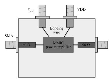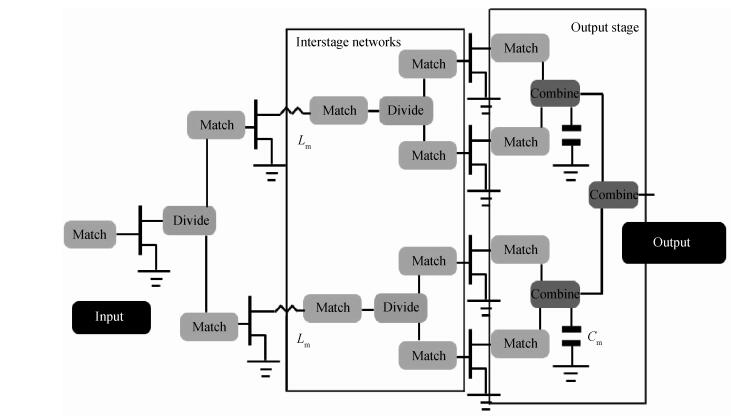
Fig. 1.
The simplified schematic circuit of the MMIC power amplifier.
SEMICONDUCTOR INTEGRATED CIRCUITS
Yifeng Chen, Jinhai Quan, Yungang Liu and Liulin Hu
Corresponding author: Chen Yifeng, Email:chenyifenguestc@126.com
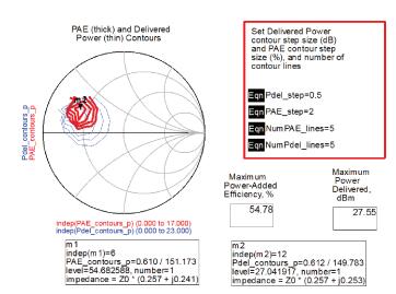
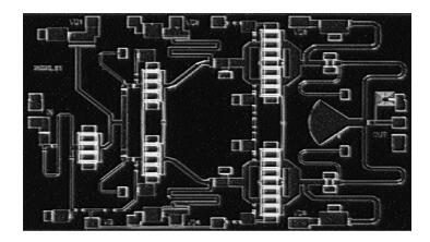
Abstract: A three-stage monolithic microwave integrated circuit (MMIC) power amplifier from 6-18 GHz, which achieves high output power with excellent efficiency, is designed, fabricated and tested. Measured results show that the saturated output power and the small signal gain are about 32 dBm and 23 dB, respectively. Thus, the power added efficiency of about 28% indicates that it is useful in various communication systems.
Keywords: power amplifier, MMIC, 6-18 GHz
| [1] |
Popovich R, Rahmanony O. Miniature 6-18 GHz switched-bit phase shifter. Microwave Review, 2004:49 https://core.ac.uk/download/pdf/11068005.pdf
|
| [2] |
Liao C F, Liu S I. A broadband noise-canceling CMOS LNA for 3.1-10.6 GHz UWB receivers. IEEE J Solid-State Circuits, 2007, 42(2):329 doi: 10.1109/JSSC.2006.889356
|
| [3] |
Van der Bent G, de Hek A P, Bessemoulin A, et al. Low-cost high-efficient 10-Watt X-band high-power amplifier. Microwaves, Communications, Antennas and Electronics Systems, 2009:1
|
| [4] |
Chu C K, Huang H K, Liu H Z, et al. A 9.1-10.7 GHz 10-W, 40-dB gain four-stage PHEMT MMIC power amplifier. IEEE Microw Wirel Comp, 2007, 17(2):151 doi: 10.1109/LMWC.2006.890346
|
| [5] |
Bannister D C, Zelley C A, Barnes A R. A 2-18 GHz wideband high dynamic range receiver MMIC. IEEE RFIC Symp Dig, 2002:147
|
| [6] |
Tzeng B, Lien C H, Wang H, et al. A 1-17-GHz InGaP-GaAs HBT MMIC analog multiplier and mixer with broad-band input-matching network. IEEE Trans Microw Theory & Tech, 2002, 50(11):2564
|
| [7] |
Chang H Y, Liu Y C, Weng S H, et al. Design and analysis of a DC-43.5-GHz fully integrated distributed amplifier using GaAs HEMT-HBT cascode gain stage. IEEE Trans Microw Theory & Tech, 2011, 59(2):443 http://www.indjst.org/index.php/indjst/article/view/101513
|
| [8] |
Kim J, Kim Y, Lee S, et al. A broadband power-reconfigurable distributed amplifier. Microwave Symposium Digest (MTT), 2012:1
|
| [9] |
Park Y, Kim Y, Choi W, et al. X-to-K band broadband watt-level power amplifier using stacked-FET unit cells. Radio Frequency Integrated Circuits Symposium (RFIC), 2011:1 doi: 10.1007/s10470-016-0819-9
|
| [10] |
http: //www. avagotech. com/docs/AV02-1370EN
|
| [11] |
http: //module-csums. cognix-systems. com/telechargement/9-1-1. pdf
|
| [12] |
Li D Z, Wang C, Huang W C, et al. A high-power Ka-bang power amplifier design based on GaAs PHEMT technology for VSAT ODU applications. 3rd IEEE International Symposium on Microwave, Antenna, Propagation and EMC Technologies for Wireless Communications, 2009:20 http://amsacta.unibo.it/1224/1/GA051555.PDF
|
| [13] |
Chaki S, Amasuga H, Goto S, et al. A V-band high power and high gain amplifier MMIC using GaAs PHEMT technology. IEEE Compound Semiconductor Integrated Circuits Symposium, 2008:1
|
| [14] |
http: //www. avagotech. com/docs/5988-2710EN
|
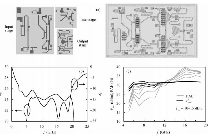
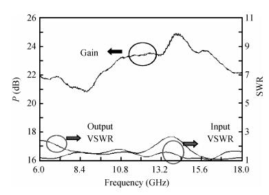
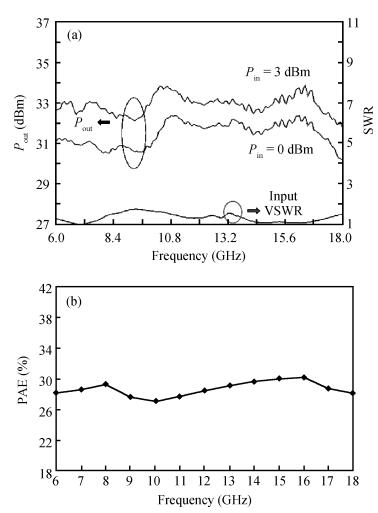
Table 1. Bias voltage of the MMIC power amplifier.

|
Table 2. Correspondence value of MCy and yield.

|
| [1] |
Popovich R, Rahmanony O. Miniature 6-18 GHz switched-bit phase shifter. Microwave Review, 2004:49 https://core.ac.uk/download/pdf/11068005.pdf
|
| [2] |
Liao C F, Liu S I. A broadband noise-canceling CMOS LNA for 3.1-10.6 GHz UWB receivers. IEEE J Solid-State Circuits, 2007, 42(2):329 doi: 10.1109/JSSC.2006.889356
|
| [3] |
Van der Bent G, de Hek A P, Bessemoulin A, et al. Low-cost high-efficient 10-Watt X-band high-power amplifier. Microwaves, Communications, Antennas and Electronics Systems, 2009:1
|
| [4] |
Chu C K, Huang H K, Liu H Z, et al. A 9.1-10.7 GHz 10-W, 40-dB gain four-stage PHEMT MMIC power amplifier. IEEE Microw Wirel Comp, 2007, 17(2):151 doi: 10.1109/LMWC.2006.890346
|
| [5] |
Bannister D C, Zelley C A, Barnes A R. A 2-18 GHz wideband high dynamic range receiver MMIC. IEEE RFIC Symp Dig, 2002:147
|
| [6] |
Tzeng B, Lien C H, Wang H, et al. A 1-17-GHz InGaP-GaAs HBT MMIC analog multiplier and mixer with broad-band input-matching network. IEEE Trans Microw Theory & Tech, 2002, 50(11):2564
|
| [7] |
Chang H Y, Liu Y C, Weng S H, et al. Design and analysis of a DC-43.5-GHz fully integrated distributed amplifier using GaAs HEMT-HBT cascode gain stage. IEEE Trans Microw Theory & Tech, 2011, 59(2):443 http://www.indjst.org/index.php/indjst/article/view/101513
|
| [8] |
Kim J, Kim Y, Lee S, et al. A broadband power-reconfigurable distributed amplifier. Microwave Symposium Digest (MTT), 2012:1
|
| [9] |
Park Y, Kim Y, Choi W, et al. X-to-K band broadband watt-level power amplifier using stacked-FET unit cells. Radio Frequency Integrated Circuits Symposium (RFIC), 2011:1 doi: 10.1007/s10470-016-0819-9
|
| [10] |
http: //www. avagotech. com/docs/AV02-1370EN
|
| [11] |
http: //module-csums. cognix-systems. com/telechargement/9-1-1. pdf
|
| [12] |
Li D Z, Wang C, Huang W C, et al. A high-power Ka-bang power amplifier design based on GaAs PHEMT technology for VSAT ODU applications. 3rd IEEE International Symposium on Microwave, Antenna, Propagation and EMC Technologies for Wireless Communications, 2009:20 http://amsacta.unibo.it/1224/1/GA051555.PDF
|
| [13] |
Chaki S, Amasuga H, Goto S, et al. A V-band high power and high gain amplifier MMIC using GaAs PHEMT technology. IEEE Compound Semiconductor Integrated Circuits Symposium, 2008:1
|
| [14] |
http: //www. avagotech. com/docs/5988-2710EN
|


Article views: 3594 Times PDF downloads: 85 Times Cited by: 0 Times
Received: 08 April 2013 Revised: 13 August 2013 Online: Published: 01 January 2014
| Citation: |
Yifeng Chen, Jinhai Quan, Yungang Liu, Liulin Hu. A 6-18 GHz broadband power amplifier MMIC with excellent efficiency[J]. Journal of Semiconductors, 2014, 35(1): 015007. doi: 10.1088/1674-4926/35/1/015007
****
Y F Chen, J H Quan, Y G Liu, L L Hu. A 6-18 GHz broadband power amplifier MMIC with excellent efficiency[J]. J. Semicond., 2014, 35(1): 015007. doi: 10.1088/1674-4926/35/1/015007.

|
| [1] |
Popovich R, Rahmanony O. Miniature 6-18 GHz switched-bit phase shifter. Microwave Review, 2004:49 https://core.ac.uk/download/pdf/11068005.pdf
|
| [2] |
Liao C F, Liu S I. A broadband noise-canceling CMOS LNA for 3.1-10.6 GHz UWB receivers. IEEE J Solid-State Circuits, 2007, 42(2):329 doi: 10.1109/JSSC.2006.889356
|
| [3] |
Van der Bent G, de Hek A P, Bessemoulin A, et al. Low-cost high-efficient 10-Watt X-band high-power amplifier. Microwaves, Communications, Antennas and Electronics Systems, 2009:1
|
| [4] |
Chu C K, Huang H K, Liu H Z, et al. A 9.1-10.7 GHz 10-W, 40-dB gain four-stage PHEMT MMIC power amplifier. IEEE Microw Wirel Comp, 2007, 17(2):151 doi: 10.1109/LMWC.2006.890346
|
| [5] |
Bannister D C, Zelley C A, Barnes A R. A 2-18 GHz wideband high dynamic range receiver MMIC. IEEE RFIC Symp Dig, 2002:147
|
| [6] |
Tzeng B, Lien C H, Wang H, et al. A 1-17-GHz InGaP-GaAs HBT MMIC analog multiplier and mixer with broad-band input-matching network. IEEE Trans Microw Theory & Tech, 2002, 50(11):2564
|
| [7] |
Chang H Y, Liu Y C, Weng S H, et al. Design and analysis of a DC-43.5-GHz fully integrated distributed amplifier using GaAs HEMT-HBT cascode gain stage. IEEE Trans Microw Theory & Tech, 2011, 59(2):443 http://www.indjst.org/index.php/indjst/article/view/101513
|
| [8] |
Kim J, Kim Y, Lee S, et al. A broadband power-reconfigurable distributed amplifier. Microwave Symposium Digest (MTT), 2012:1
|
| [9] |
Park Y, Kim Y, Choi W, et al. X-to-K band broadband watt-level power amplifier using stacked-FET unit cells. Radio Frequency Integrated Circuits Symposium (RFIC), 2011:1 doi: 10.1007/s10470-016-0819-9
|
| [10] |
http: //www. avagotech. com/docs/AV02-1370EN
|
| [11] |
http: //module-csums. cognix-systems. com/telechargement/9-1-1. pdf
|
| [12] |
Li D Z, Wang C, Huang W C, et al. A high-power Ka-bang power amplifier design based on GaAs PHEMT technology for VSAT ODU applications. 3rd IEEE International Symposium on Microwave, Antenna, Propagation and EMC Technologies for Wireless Communications, 2009:20 http://amsacta.unibo.it/1224/1/GA051555.PDF
|
| [13] |
Chaki S, Amasuga H, Goto S, et al. A V-band high power and high gain amplifier MMIC using GaAs PHEMT technology. IEEE Compound Semiconductor Integrated Circuits Symposium, 2008:1
|
| [14] |
http: //www. avagotech. com/docs/5988-2710EN
|

 WeChat ID
Journal of Semiconductors © 2017 All Rights Reserved 京ICP备05085259号-2

 DownLoad: