Fig. 1.
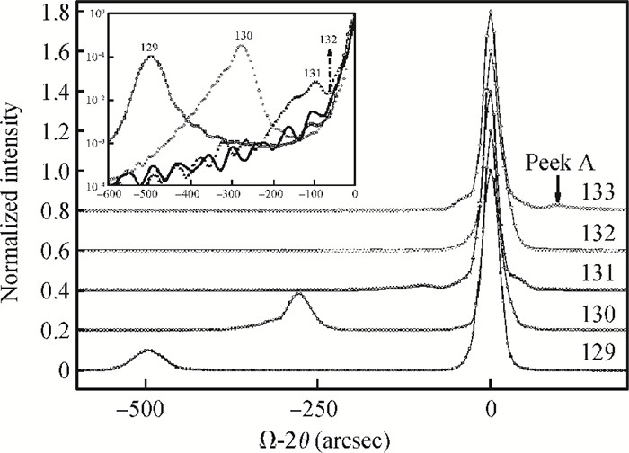
XRD curves for GaInP layers with increasing Ga-content in samples 129–132, sample 133 is a broad band TJ.
SEMICONDUCTOR MATERIALS
Hongbo Lu, Jingman Shen, Xinyi Li, Wei Zhang, Dayong Zhou, Lijie Sun and Kaijian Chen
Corresponding author: Lu Hongbo, Email:lhb2139@163.com
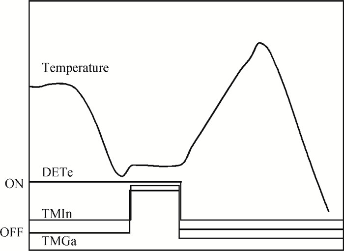
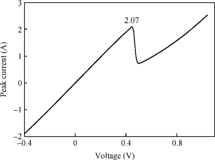
Abstract: A GaInP/AlGaAs broadband tunnel junction (TJ) with a peak current density of 65.3 A/cm2 and an AlGaInP/AlGaAs ultrabroad band TJ with a peak current density of 6.1 A/cm2 were studied and fabricated. Diethyltellurium (DETe) was chosen as an n-type dopant in the TJ. The growth temperature, valve switching and flow variation parameters of DETe were studied for better performance. Measurements, including predoping of DETe before growth and heating up reactor temperature after growth, were taken to deal with the effect of turn-on and off of tellurium. The strain balance method was used to the manage lattice mismatch that was introduced by the tellurium. Various flows of DETe were studied to get the appropriate value needed to fabricate a high peak current density tunnel junction.
Keywords: tunnel junction, solar cell, broadband
| [1] |
Chiu P T, Law D C, Woo R L, et al. Direct semiconductor bonded 5J cell for space and terrestrial applications. IEEE Journal of Photovoltaics, 2014, 4(1):493 doi: 10.1109/JPHOTOV.2013.2279336
|
| [2] |
Ebert C, Pulwin Z, Byrnes D. Tellurium doping of InGaP for tunnel junction applications in triple junction solar cells. J Cryst Growth, 2011, 315:61 doi: 10.1016/j.jcrysgro.2010.09.050
|
| [3] |
Garcia I, Rey-Stolle I, Galiana B, et al. Analysis of tellurium as n-type dopant in GaInP:doping, diffusion, memory effect and surfactant properties. J Cryst Growth, 2007, 298:794 doi: 10.1016/j.jcrysgro.2006.10.099
|
| [4] |
Stringfellow G B, Shurtle J K, Lee R T, et al. Surface processes in OMVPE-the frontiers. J Cryst Growth, 2000, 221:1 doi: 10.1016/S0022-0248(00)00640-0
|
| [5] |
Jun S W, Stringfellow G B, Howard A D, et al. Kinetics of Te doping in disordering GaInP grown by organometallic vapor phase epitaxy. J Appl Phys, 2001, 90:6048 doi: 10.1063/1.1416857
|
| [6] |
Forbes D V, Bailey C G, Polly, et al. The effect of TE as a surfactant on OMVPE of InAs quantum dots. 34th PVSC, 2009:400 http://ieeexplore.ieee.org/document/5411654/?arnumber=5411654&filter%3DAND(p_IS_Number:5411118)
|
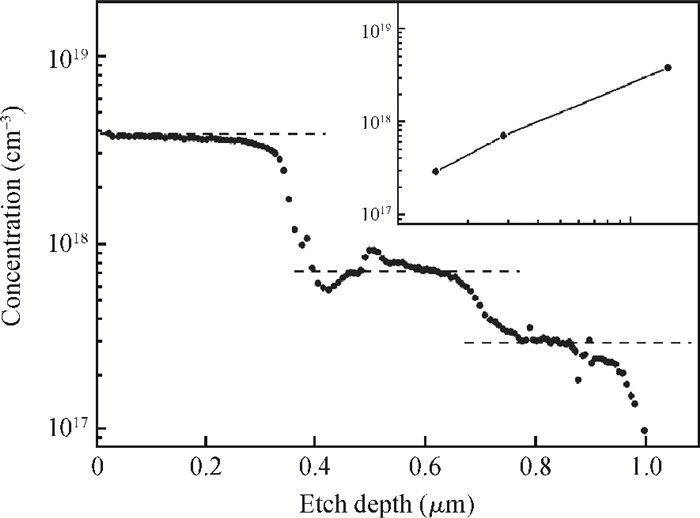
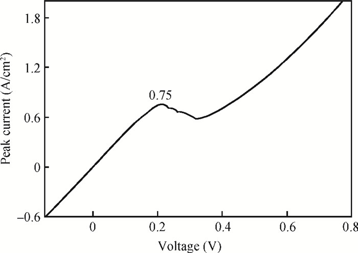
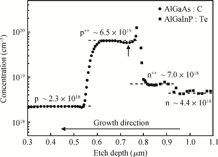
Table 1. Doping concentration GaInP under different DETe flows.

|
| [1] |
Chiu P T, Law D C, Woo R L, et al. Direct semiconductor bonded 5J cell for space and terrestrial applications. IEEE Journal of Photovoltaics, 2014, 4(1):493 doi: 10.1109/JPHOTOV.2013.2279336
|
| [2] |
Ebert C, Pulwin Z, Byrnes D. Tellurium doping of InGaP for tunnel junction applications in triple junction solar cells. J Cryst Growth, 2011, 315:61 doi: 10.1016/j.jcrysgro.2010.09.050
|
| [3] |
Garcia I, Rey-Stolle I, Galiana B, et al. Analysis of tellurium as n-type dopant in GaInP:doping, diffusion, memory effect and surfactant properties. J Cryst Growth, 2007, 298:794 doi: 10.1016/j.jcrysgro.2006.10.099
|
| [4] |
Stringfellow G B, Shurtle J K, Lee R T, et al. Surface processes in OMVPE-the frontiers. J Cryst Growth, 2000, 221:1 doi: 10.1016/S0022-0248(00)00640-0
|
| [5] |
Jun S W, Stringfellow G B, Howard A D, et al. Kinetics of Te doping in disordering GaInP grown by organometallic vapor phase epitaxy. J Appl Phys, 2001, 90:6048 doi: 10.1063/1.1416857
|
| [6] |
Forbes D V, Bailey C G, Polly, et al. The effect of TE as a surfactant on OMVPE of InAs quantum dots. 34th PVSC, 2009:400 http://ieeexplore.ieee.org/document/5411654/?arnumber=5411654&filter%3DAND(p_IS_Number:5411118)
|


Article views: 3399 Times PDF downloads: 33 Times Cited by: 0 Times
Received: 02 January 2014 Revised: 01 April 2014 Online: Published: 01 October 2014
| Citation: |
Hongbo Lu, Jingman Shen, Xinyi Li, Wei Zhang, Dayong Zhou, Lijie Sun, Kaijian Chen. Te doped ultrabroad band tunnel junction[J]. Journal of Semiconductors, 2014, 35(10): 103003. doi: 10.1088/1674-4926/35/10/103003
****
H B Lu, J M Shen, X Y Li, W Zhang, D Y Zhou, L J Sun, K J Chen. Te doped ultrabroad band tunnel junction[J]. J. Semicond., 2014, 35(10): 103003. doi: 10.1088/1674-4926/35/10/103003.

|
| [1] |
Chiu P T, Law D C, Woo R L, et al. Direct semiconductor bonded 5J cell for space and terrestrial applications. IEEE Journal of Photovoltaics, 2014, 4(1):493 doi: 10.1109/JPHOTOV.2013.2279336
|
| [2] |
Ebert C, Pulwin Z, Byrnes D. Tellurium doping of InGaP for tunnel junction applications in triple junction solar cells. J Cryst Growth, 2011, 315:61 doi: 10.1016/j.jcrysgro.2010.09.050
|
| [3] |
Garcia I, Rey-Stolle I, Galiana B, et al. Analysis of tellurium as n-type dopant in GaInP:doping, diffusion, memory effect and surfactant properties. J Cryst Growth, 2007, 298:794 doi: 10.1016/j.jcrysgro.2006.10.099
|
| [4] |
Stringfellow G B, Shurtle J K, Lee R T, et al. Surface processes in OMVPE-the frontiers. J Cryst Growth, 2000, 221:1 doi: 10.1016/S0022-0248(00)00640-0
|
| [5] |
Jun S W, Stringfellow G B, Howard A D, et al. Kinetics of Te doping in disordering GaInP grown by organometallic vapor phase epitaxy. J Appl Phys, 2001, 90:6048 doi: 10.1063/1.1416857
|
| [6] |
Forbes D V, Bailey C G, Polly, et al. The effect of TE as a surfactant on OMVPE of InAs quantum dots. 34th PVSC, 2009:400 http://ieeexplore.ieee.org/document/5411654/?arnumber=5411654&filter%3DAND(p_IS_Number:5411118)
|

 WeChat ID
Journal of Semiconductors © 2017 All Rights Reserved 京ICP备05085259号-2

 DownLoad: