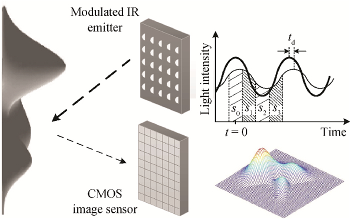
Fig. 1.
ToF camera setup for depth measurement.
SEMICONDUCTOR INTEGRATED CIRCUITS
Zhe Chen, Shan Di, Cong Shi, Liyuan Liu and Nanjian Wu
Corresponding author: Nanjian Wu, Email:nanjian@semi.ac.cn
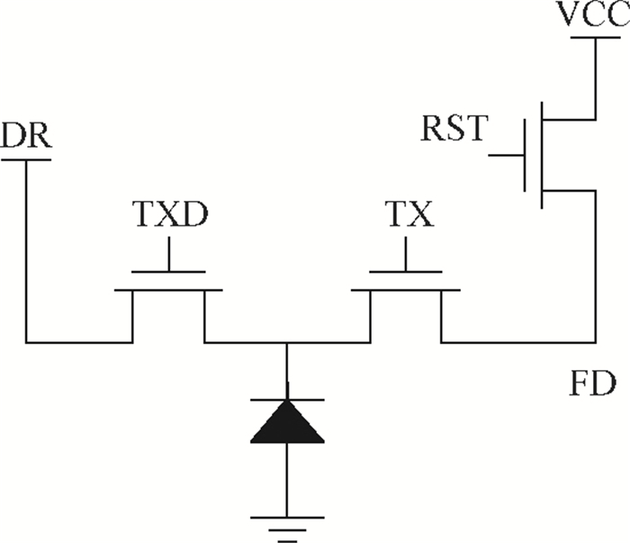
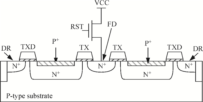
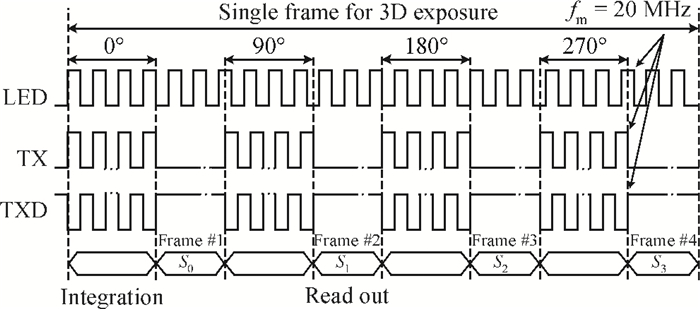
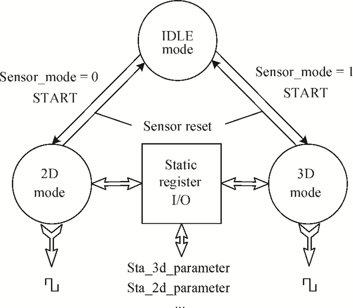
Abstract: This paper presents an image sensor controller that is compatible for depth measurement, which is based on the continuous-wave modulation time-of-flight technology. The image sensor controller is utilized to generate reconfigurable control signals for a 256×256 high speed CMOS image sensor with a conventional image sensing mode and a depth measurement mode. The image sensor controller generates control signals for the pixel array to realize the rolling exposure and the correlated double sampling functions. An refined circuit design technique in the logic level is presented to reduce chip area and power consumption. The chip, with a size of 700×3380 μm2, is fabricated in a standard 0.18 μm CMOS image sensor process. The power consumption estimated by the synthesis tool is 65 mW under a 1.8 V supply voltage and a 100 MHz clock frequency. Our test results show that the image sensor controller functions properly.
Keywords: CMOS image sensor, depth measurement, time-of-flight
| [1] |
Coren S, Ward L M, Enns J T. Sensation and perception. Harcourt Brace College Publishers, 1994
|
| [2] |
Mikhail E M, Betherl J S, McGlone J C. Introduction to modern photogrammetry. New York: John Wiley & Sons, Inc. , 2001
|
| [3] |
Remondino F, Stoppa D. TOF range-imaging cameras. Springer, 2013
|
| [4] |
Spirig T, Seitz P, Vietze O, et al. The lock-in CCD-two-dimensional synchronous detection of light. IEEE J Quantum Electron, 1995, 31(9):1705 doi: 10.1109/3.406386
|
| [5] |
Lange R, Seitz P. Solid-state time-of-flight range camera. IEEE J Quantum Electron, 2001, 37(3):390 doi: 10.1109/3.910448
|
| [6] |
Foix S, Alenya G, Torras C. Lock-in time-of-flight (ToF) cameras:a survey. IEEE Sensors J, 2011, 11(9):1917 doi: 10.1109/JSEN.2010.2101060
|
| [7] |
Perenzoni M, Massari N, Stoppa D, et al. A 160×120-pixels range camera with in-pixel correlated double sampling and fixed-pattern noise correction. IEEE J Solid-State Circuits, 2011, 46(7):1672 doi: 10.1109/JSSC.2011.2144130
|
| [8] |
Jin K S, Kim J D K, Byongmin K, et al. A CMOS image sensor based on unified pixel architecture with time-division multiplexing scheme for color and depth image acquisition. IEEE J Solid-State Circuits, 2012, 47(11):2834 doi: 10.1109/JSSC.2012.2214179
|
| [9] |
Stoppa D, Massari N, Pancheri L, et al. A range image sensor based on 10-μm lock-in pixels in 0.18μm CMOS imaging technology. IEEE J Solid-State Circuits, 2011, 46(1):248 doi: 10.1109/JSSC.2010.2085870
|
| [10] |
Jin K S, Byongmin K, Kim J D K, et al. A 1920×10803. 65μm-pixel 2D/3D image sensor with split and binning pixel structure in 0. 11μm standard CMOS. ISSCC Dig Tech Papers, 2012: 396
|
| [11] |
Niclass C, Favi C, Kluter T, et al. A 128×128 single-photon image sensor with column-level 10-bit time-to-digital converter array. IEEE J Solid-State Circuits, 2008, 43(12):2977 doi: 10.1109/JSSC.2008.2006445
|
| [12] |
Niclass C, Favi C, Kluter T, et al. Single-photon synchronous detection. IEEE J Solid-State Circuits, 2009, 44(7):1977 doi: 10.1109/JSSC.2009.2021920
|
| [13] |
Stoppa D, Pancheri L, Scandiuzzo M, et al. A CMOS 3-D imager based on single photon avalanche diode. IEEE Trans Circuits Syst Ⅰ, Reg Papers, 2007, 54(1):4 doi: 10.1109/TCSI.2006.888679
|
| [14] |
Niclass C, Soga M, Matsubara H, et al. A 100-m range 10-frame/s 340×96-pixel time-of-flight depth sensor in 0.18-μm CMOS. IEEE J Solid-State Circuits, 2013, 48(2):559 doi: 10.1109/JSSC.2012.2227607
|
| [15] |
Niclass C, Soga M, Matsubara H, et al. A 0.18-μm CMOS SoC for a 100-m-range 10-frame/s 200×96-pixel time-of-flight depth sensor. IEEE J Solid-State Circuits, 2014, 49(1):315 doi: 10.1109/JSSC.2013.2284352
|
| [16] |
Cao Zhongxiang, Zhou Yangfan, Li Quanliang, et al. Design of pixel for high speed CMOS image sensors. International Image Sensor Workshop, 2013
|
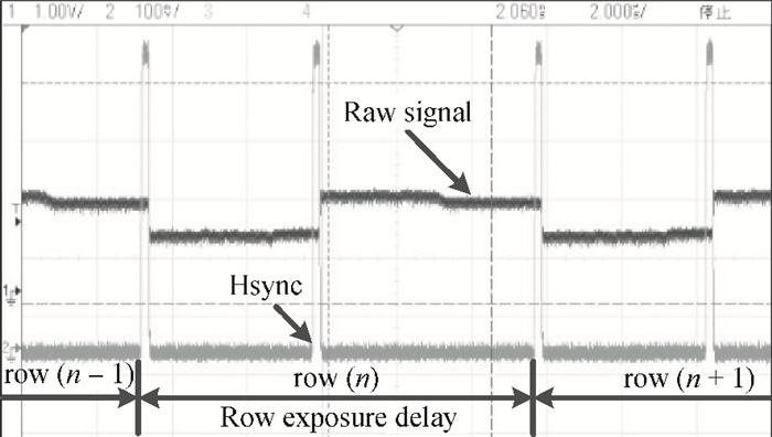
Table 1. List of partial reconfigurable parameters of the image sensor controller.

|
| [1] |
Coren S, Ward L M, Enns J T. Sensation and perception. Harcourt Brace College Publishers, 1994
|
| [2] |
Mikhail E M, Betherl J S, McGlone J C. Introduction to modern photogrammetry. New York: John Wiley & Sons, Inc. , 2001
|
| [3] |
Remondino F, Stoppa D. TOF range-imaging cameras. Springer, 2013
|
| [4] |
Spirig T, Seitz P, Vietze O, et al. The lock-in CCD-two-dimensional synchronous detection of light. IEEE J Quantum Electron, 1995, 31(9):1705 doi: 10.1109/3.406386
|
| [5] |
Lange R, Seitz P. Solid-state time-of-flight range camera. IEEE J Quantum Electron, 2001, 37(3):390 doi: 10.1109/3.910448
|
| [6] |
Foix S, Alenya G, Torras C. Lock-in time-of-flight (ToF) cameras:a survey. IEEE Sensors J, 2011, 11(9):1917 doi: 10.1109/JSEN.2010.2101060
|
| [7] |
Perenzoni M, Massari N, Stoppa D, et al. A 160×120-pixels range camera with in-pixel correlated double sampling and fixed-pattern noise correction. IEEE J Solid-State Circuits, 2011, 46(7):1672 doi: 10.1109/JSSC.2011.2144130
|
| [8] |
Jin K S, Kim J D K, Byongmin K, et al. A CMOS image sensor based on unified pixel architecture with time-division multiplexing scheme for color and depth image acquisition. IEEE J Solid-State Circuits, 2012, 47(11):2834 doi: 10.1109/JSSC.2012.2214179
|
| [9] |
Stoppa D, Massari N, Pancheri L, et al. A range image sensor based on 10-μm lock-in pixels in 0.18μm CMOS imaging technology. IEEE J Solid-State Circuits, 2011, 46(1):248 doi: 10.1109/JSSC.2010.2085870
|
| [10] |
Jin K S, Byongmin K, Kim J D K, et al. A 1920×10803. 65μm-pixel 2D/3D image sensor with split and binning pixel structure in 0. 11μm standard CMOS. ISSCC Dig Tech Papers, 2012: 396
|
| [11] |
Niclass C, Favi C, Kluter T, et al. A 128×128 single-photon image sensor with column-level 10-bit time-to-digital converter array. IEEE J Solid-State Circuits, 2008, 43(12):2977 doi: 10.1109/JSSC.2008.2006445
|
| [12] |
Niclass C, Favi C, Kluter T, et al. Single-photon synchronous detection. IEEE J Solid-State Circuits, 2009, 44(7):1977 doi: 10.1109/JSSC.2009.2021920
|
| [13] |
Stoppa D, Pancheri L, Scandiuzzo M, et al. A CMOS 3-D imager based on single photon avalanche diode. IEEE Trans Circuits Syst Ⅰ, Reg Papers, 2007, 54(1):4 doi: 10.1109/TCSI.2006.888679
|
| [14] |
Niclass C, Soga M, Matsubara H, et al. A 100-m range 10-frame/s 340×96-pixel time-of-flight depth sensor in 0.18-μm CMOS. IEEE J Solid-State Circuits, 2013, 48(2):559 doi: 10.1109/JSSC.2012.2227607
|
| [15] |
Niclass C, Soga M, Matsubara H, et al. A 0.18-μm CMOS SoC for a 100-m-range 10-frame/s 200×96-pixel time-of-flight depth sensor. IEEE J Solid-State Circuits, 2014, 49(1):315 doi: 10.1109/JSSC.2013.2284352
|
| [16] |
Cao Zhongxiang, Zhou Yangfan, Li Quanliang, et al. Design of pixel for high speed CMOS image sensors. International Image Sensor Workshop, 2013
|


Article views: 4699 Times PDF downloads: 31 Times Cited by: 0 Times
Received: 18 February 2014 Revised: 21 April 2014 Online: Published: 01 October 2014
| Citation: |
Zhe Chen, Shan Di, Cong Shi, Liyuan Liu, Nanjian Wu. A reconfigurable 256 × 256 image sensor controller that is compatible for depth measurement[J]. Journal of Semiconductors, 2014, 35(10): 105007. doi: 10.1088/1674-4926/35/10/105007
****
Z Chen, S Di, C Shi, L Y Liu, N J Wu. A reconfigurable 256 × 256 image sensor controller that is compatible for depth measurement[J]. J. Semicond., 2014, 35(10): 105007. doi: 10.1088/1674-4926/35/10/105007.

|
| [1] |
Coren S, Ward L M, Enns J T. Sensation and perception. Harcourt Brace College Publishers, 1994
|
| [2] |
Mikhail E M, Betherl J S, McGlone J C. Introduction to modern photogrammetry. New York: John Wiley & Sons, Inc. , 2001
|
| [3] |
Remondino F, Stoppa D. TOF range-imaging cameras. Springer, 2013
|
| [4] |
Spirig T, Seitz P, Vietze O, et al. The lock-in CCD-two-dimensional synchronous detection of light. IEEE J Quantum Electron, 1995, 31(9):1705 doi: 10.1109/3.406386
|
| [5] |
Lange R, Seitz P. Solid-state time-of-flight range camera. IEEE J Quantum Electron, 2001, 37(3):390 doi: 10.1109/3.910448
|
| [6] |
Foix S, Alenya G, Torras C. Lock-in time-of-flight (ToF) cameras:a survey. IEEE Sensors J, 2011, 11(9):1917 doi: 10.1109/JSEN.2010.2101060
|
| [7] |
Perenzoni M, Massari N, Stoppa D, et al. A 160×120-pixels range camera with in-pixel correlated double sampling and fixed-pattern noise correction. IEEE J Solid-State Circuits, 2011, 46(7):1672 doi: 10.1109/JSSC.2011.2144130
|
| [8] |
Jin K S, Kim J D K, Byongmin K, et al. A CMOS image sensor based on unified pixel architecture with time-division multiplexing scheme for color and depth image acquisition. IEEE J Solid-State Circuits, 2012, 47(11):2834 doi: 10.1109/JSSC.2012.2214179
|
| [9] |
Stoppa D, Massari N, Pancheri L, et al. A range image sensor based on 10-μm lock-in pixels in 0.18μm CMOS imaging technology. IEEE J Solid-State Circuits, 2011, 46(1):248 doi: 10.1109/JSSC.2010.2085870
|
| [10] |
Jin K S, Byongmin K, Kim J D K, et al. A 1920×10803. 65μm-pixel 2D/3D image sensor with split and binning pixel structure in 0. 11μm standard CMOS. ISSCC Dig Tech Papers, 2012: 396
|
| [11] |
Niclass C, Favi C, Kluter T, et al. A 128×128 single-photon image sensor with column-level 10-bit time-to-digital converter array. IEEE J Solid-State Circuits, 2008, 43(12):2977 doi: 10.1109/JSSC.2008.2006445
|
| [12] |
Niclass C, Favi C, Kluter T, et al. Single-photon synchronous detection. IEEE J Solid-State Circuits, 2009, 44(7):1977 doi: 10.1109/JSSC.2009.2021920
|
| [13] |
Stoppa D, Pancheri L, Scandiuzzo M, et al. A CMOS 3-D imager based on single photon avalanche diode. IEEE Trans Circuits Syst Ⅰ, Reg Papers, 2007, 54(1):4 doi: 10.1109/TCSI.2006.888679
|
| [14] |
Niclass C, Soga M, Matsubara H, et al. A 100-m range 10-frame/s 340×96-pixel time-of-flight depth sensor in 0.18-μm CMOS. IEEE J Solid-State Circuits, 2013, 48(2):559 doi: 10.1109/JSSC.2012.2227607
|
| [15] |
Niclass C, Soga M, Matsubara H, et al. A 0.18-μm CMOS SoC for a 100-m-range 10-frame/s 200×96-pixel time-of-flight depth sensor. IEEE J Solid-State Circuits, 2014, 49(1):315 doi: 10.1109/JSSC.2013.2284352
|
| [16] |
Cao Zhongxiang, Zhou Yangfan, Li Quanliang, et al. Design of pixel for high speed CMOS image sensors. International Image Sensor Workshop, 2013
|

 WeChat ID
Journal of Semiconductors © 2017 All Rights Reserved 京ICP备05085259号-2

 DownLoad: