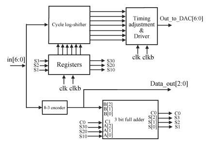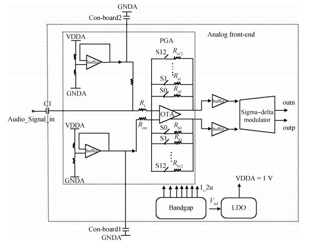
Fig. 1.
Block diagram of AFE
SEMICONDUCTOR INTEGRATED CIRCUITS
Lan Dai, Wenkai Liu and Yan Lu
Corresponding author: Dai Lan, Email:perfect_dai@163.com
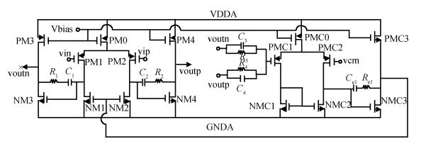
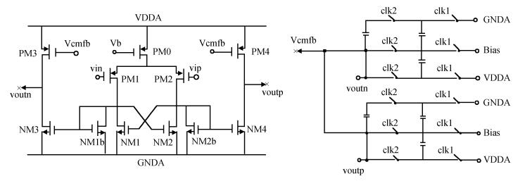
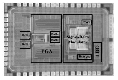
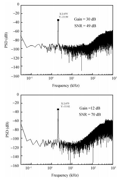
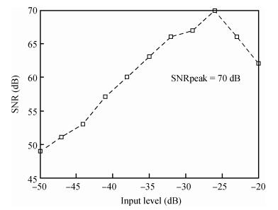
Abstract: This paper describes an analog front-end (AFE) intended for portable audio application, which operates at 1 V and consumes only 410 μW. The AFE consists of a 30 dB-gain programmable gain amplifier (PGA) and a 2nd-order 3-bit sigma-delta modulator. The PGA with single input and on-chip common-mode bias voltage shows good noise-reduction performance. The modulator makes use of data weighted averaging to reduce the linearity requirements of the digital-to-analog converter in the feedback loop. The AFE is implemented in the SMIC 0.13 μm 1P8M CMOS process. The measurement results show that in a 1 V power supply, at 200 mVp-p, between 100 Hz and 20 kHz, the maximal signal-to-noise ratio is 70 dB, and the total power is 410 μW.
Keywords: analog front-end, low power, PGA, modulator
| [1] |
Marques A, Peluso V, Steyaert M, et al. Optimal parameters for sigma-delta modulator topologies. IEEE Trans Circuit Syst, 1998, 45:1232 doi: 10.1109/82.718590
|
| [2] |
Geert Y, Steyaert M, Sansenl W. A high-performance multibit sigma-delta CMOS ADC. IEEE J Solid-State Circuits, 2000, 35(12):1829 doi: 10.1109/4.890296
|
| [3] |
Silva M J, Solis B S, Schellenberg M. A CMOS hearing aid device. Analog Integrated Circuit and Signal Processing, 1999, 21(2):163 doi: 10.1023/A:1008373824380
|
| [4] |
Graells F, Gomez L, Huertas J. A true-1-V 300-μW CMOS-subthreshold log-dommain hearing-aid-on-chip. IEEE J Solid-State Circuits, 2004, 39(8):1271 doi: 10.1109/JSSC.2004.831469
|
| [5] |
Wayne D, Rives M, Huynh T, et al. A single-chip hearing aid with one volt switched-capacitor filters. Proc IEEE Custom Integrated Circuits Conf, May 1992: 751
|
| [6] |
Nerteboom H, Janssens M A E, Leenen J R G M, et al. A single battery 0.9 V-operated digital sound processing IC including AD/DA and IR receiver with 2 mW power consumption. IEEE Int Solid-State Circuit Conf Dig Tech Paper, 1997:98
|
| [7] |
Miller M, Petriel C. A multibit sigma-delta ADC for multimode receivers. IEEE J Solid-State Circuits, 2003, 38(3):475 doi: 10.1109/JSSC.2002.808321
|
| [8] |
Kim S, Lee J Y, Song S J, et al. An energy-efficient analog front-end circuit for a sub-1 V digital hearing aid. IEEE J Solid-State Circuits, 2006, 41(4):876 doi: 10.1109/JSSC.2006.870798
|
| [9] |
Gata D, Sjursen W, Hochschild J, et al. A 1.1-V 270-μA mixed-signal hearing aid chip. IEEE J Solid-State Circuits, 2002, 37(12):1670 doi: 10.1109/JSSC.2002.804328
|
| [10] |
Kim S Y, Cho N J, Song S J, et al. A 0.9 V 96μW fully operational digital hearing aid chip. IEEE J Solid-State Circuits, 2007, 42(11):2432 doi: 10.1109/JSSC.2007.907198
|
| [11] |
Sukumaran A, Karanjkar K, Jhanwar S, et al. A 1.2 V 285μA analog front end chip for a digital hearing aid in 0.13μm CMOS. Proceedings of the IEEE Asian Solid-State Circuits Conference, 2013:397
|
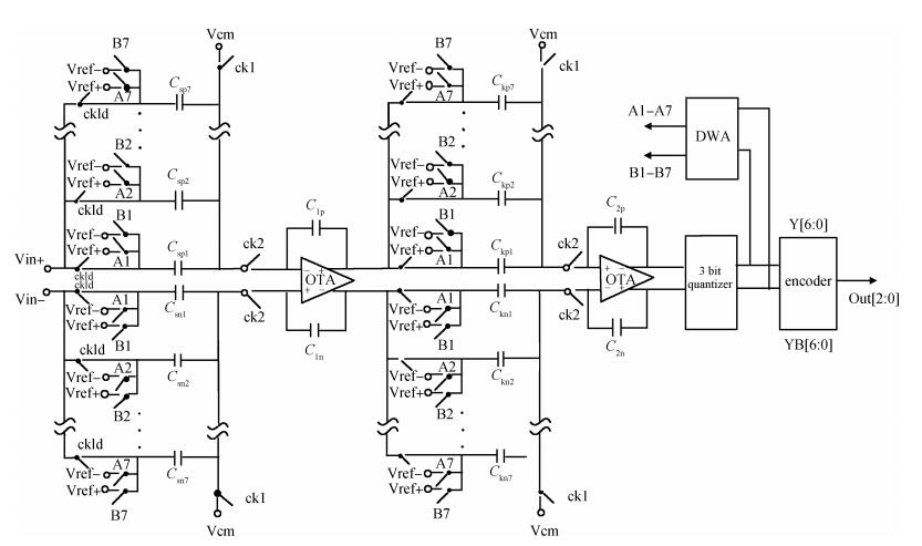
Table 1. Performance summary of AFE

|
Table 2. Performance comparison of analog front-end

|
| [1] |
Marques A, Peluso V, Steyaert M, et al. Optimal parameters for sigma-delta modulator topologies. IEEE Trans Circuit Syst, 1998, 45:1232 doi: 10.1109/82.718590
|
| [2] |
Geert Y, Steyaert M, Sansenl W. A high-performance multibit sigma-delta CMOS ADC. IEEE J Solid-State Circuits, 2000, 35(12):1829 doi: 10.1109/4.890296
|
| [3] |
Silva M J, Solis B S, Schellenberg M. A CMOS hearing aid device. Analog Integrated Circuit and Signal Processing, 1999, 21(2):163 doi: 10.1023/A:1008373824380
|
| [4] |
Graells F, Gomez L, Huertas J. A true-1-V 300-μW CMOS-subthreshold log-dommain hearing-aid-on-chip. IEEE J Solid-State Circuits, 2004, 39(8):1271 doi: 10.1109/JSSC.2004.831469
|
| [5] |
Wayne D, Rives M, Huynh T, et al. A single-chip hearing aid with one volt switched-capacitor filters. Proc IEEE Custom Integrated Circuits Conf, May 1992: 751
|
| [6] |
Nerteboom H, Janssens M A E, Leenen J R G M, et al. A single battery 0.9 V-operated digital sound processing IC including AD/DA and IR receiver with 2 mW power consumption. IEEE Int Solid-State Circuit Conf Dig Tech Paper, 1997:98
|
| [7] |
Miller M, Petriel C. A multibit sigma-delta ADC for multimode receivers. IEEE J Solid-State Circuits, 2003, 38(3):475 doi: 10.1109/JSSC.2002.808321
|
| [8] |
Kim S, Lee J Y, Song S J, et al. An energy-efficient analog front-end circuit for a sub-1 V digital hearing aid. IEEE J Solid-State Circuits, 2006, 41(4):876 doi: 10.1109/JSSC.2006.870798
|
| [9] |
Gata D, Sjursen W, Hochschild J, et al. A 1.1-V 270-μA mixed-signal hearing aid chip. IEEE J Solid-State Circuits, 2002, 37(12):1670 doi: 10.1109/JSSC.2002.804328
|
| [10] |
Kim S Y, Cho N J, Song S J, et al. A 0.9 V 96μW fully operational digital hearing aid chip. IEEE J Solid-State Circuits, 2007, 42(11):2432 doi: 10.1109/JSSC.2007.907198
|
| [11] |
Sukumaran A, Karanjkar K, Jhanwar S, et al. A 1.2 V 285μA analog front end chip for a digital hearing aid in 0.13μm CMOS. Proceedings of the IEEE Asian Solid-State Circuits Conference, 2013:397
|


Article views: 3308 Times PDF downloads: 29 Times Cited by: 0 Times
Received: 15 April 2014 Revised: 08 May 2014 Online: Published: 01 October 2014
| Citation: |
Lan Dai, Wenkai Liu, Yan Lu. A 410 μW, 70 dB SNR high performance analog front-end for portable audio application[J]. Journal of Semiconductors, 2014, 35(10): 105013. doi: 10.1088/1674-4926/35/10/105013
****
L Dai, W K Liu, Y Lu. A 410 μW, 70 dB SNR high performance analog front-end for portable audio application[J]. J. Semicond., 2014, 35(10): 105013. doi: 10.1088/1674-4926/35/10/105013.

|
| [1] |
Marques A, Peluso V, Steyaert M, et al. Optimal parameters for sigma-delta modulator topologies. IEEE Trans Circuit Syst, 1998, 45:1232 doi: 10.1109/82.718590
|
| [2] |
Geert Y, Steyaert M, Sansenl W. A high-performance multibit sigma-delta CMOS ADC. IEEE J Solid-State Circuits, 2000, 35(12):1829 doi: 10.1109/4.890296
|
| [3] |
Silva M J, Solis B S, Schellenberg M. A CMOS hearing aid device. Analog Integrated Circuit and Signal Processing, 1999, 21(2):163 doi: 10.1023/A:1008373824380
|
| [4] |
Graells F, Gomez L, Huertas J. A true-1-V 300-μW CMOS-subthreshold log-dommain hearing-aid-on-chip. IEEE J Solid-State Circuits, 2004, 39(8):1271 doi: 10.1109/JSSC.2004.831469
|
| [5] |
Wayne D, Rives M, Huynh T, et al. A single-chip hearing aid with one volt switched-capacitor filters. Proc IEEE Custom Integrated Circuits Conf, May 1992: 751
|
| [6] |
Nerteboom H, Janssens M A E, Leenen J R G M, et al. A single battery 0.9 V-operated digital sound processing IC including AD/DA and IR receiver with 2 mW power consumption. IEEE Int Solid-State Circuit Conf Dig Tech Paper, 1997:98
|
| [7] |
Miller M, Petriel C. A multibit sigma-delta ADC for multimode receivers. IEEE J Solid-State Circuits, 2003, 38(3):475 doi: 10.1109/JSSC.2002.808321
|
| [8] |
Kim S, Lee J Y, Song S J, et al. An energy-efficient analog front-end circuit for a sub-1 V digital hearing aid. IEEE J Solid-State Circuits, 2006, 41(4):876 doi: 10.1109/JSSC.2006.870798
|
| [9] |
Gata D, Sjursen W, Hochschild J, et al. A 1.1-V 270-μA mixed-signal hearing aid chip. IEEE J Solid-State Circuits, 2002, 37(12):1670 doi: 10.1109/JSSC.2002.804328
|
| [10] |
Kim S Y, Cho N J, Song S J, et al. A 0.9 V 96μW fully operational digital hearing aid chip. IEEE J Solid-State Circuits, 2007, 42(11):2432 doi: 10.1109/JSSC.2007.907198
|
| [11] |
Sukumaran A, Karanjkar K, Jhanwar S, et al. A 1.2 V 285μA analog front end chip for a digital hearing aid in 0.13μm CMOS. Proceedings of the IEEE Asian Solid-State Circuits Conference, 2013:397
|

 WeChat ID
Journal of Semiconductors © 2017 All Rights Reserved 京ICP备05085259号-2

 DownLoad: