Fig. 1.
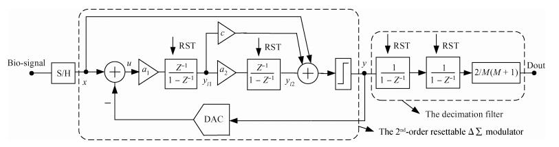
A block diagram of the second-order incremental ADC
SEMICONDUCTOR INTEGRATED CIRCUITS
Ting Huang1, Lele Jin1, Hui Li1, Shengxi Diao1, Guoxing Wang3, Libin Yao2 and Lin He1,
Corresponding author: He Lin, Email:helin77@ustc.edu.cn
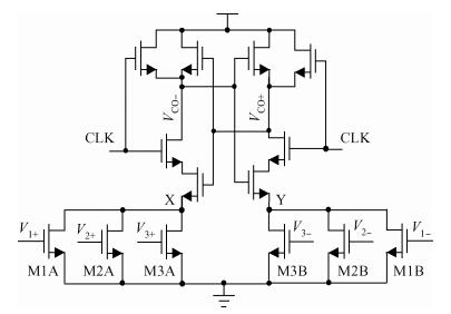
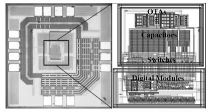
Abstract: This paper presents an ultra-low power incremental ADC for biosensor interface circuits. The ADC consists of a resettable second-order delta-sigma (Δ Σ) modulator core and a resettable decimation filter. Several techniques are adopted to minimize its power consumption. A feedforward path is introduced to the modulator core to relax the signal swing and linearity requirement of the integrators. A correlated-double-sampling (CDS) technique is applied to reject the offset and 1/f noise, thereby removing the integrator leakage and relaxing the gain requirement of the OTA. A simple double-tailed inverter-based fully differential OTA using a thick-oxide CMOS is proposed to operate in the subthreshold region to fulfill both an ultra-low power and a large output swing at 1.2 V supply. The signal addition before the comparator in the feedforward architecture is performed in the current domain instead of the voltage domain to minimize the capacitive load to the integrators. The capacitors used in this design are of customized metal-oxide-metal (MOM) type to reach the minimum capacitance set by the kT/C noise limit. Fabricated with a 1P6M 0.18 μm CMOS technology, the presented incremental ADC consumes 600 nW at 2 kS/s from a 1.2 V supply, and achieves 68.3 dB signal to noise and distortion ratio (SNDR) at the Nyquist frequency and an FOM of 0.14 pJ/conversion step. The core area is 100×120 μm2.
Keywords: ADC, incremental ADC, feedforward, inverter-based OTA, biosensor
| [1] |
Harrison R R, Watkins P T, Kier R J, et al. A low-power integrated circuit for a wireless 100-electrode neural recording system. IEEE J Solid-State Circuits, 2007, 42(1):123 doi: 10.1109/JSSC.2006.886567
|
| [2] |
Zou X, Xu X, Yao L, et al. A 1-V 450-nW fully integrated programmable biomedical sensor interface chip. IEEE J Solid-State Circuits, 2009, 44(4):1067 doi: 10.1109/JSSC.2009.2014707
|
| [3] |
Chang Y K, Wang C S, Wang C K. A 8-bit 500-KS/s low power SAR ADC for bio-medical applications. IEEE Asian Solid-State Circuits Conference (ASSCC), 2007:228
|
| [4] |
Chen C H, Crop J, Chae J, et al. A 12-bit 7μW/channel 1 kHz/channel incremental ADC for biosensor interface circuits. IEEE Int Symp Circuits and Systems (ISCAS), 2012:2969
|
| [5] |
Yu W, Aslan M, Gabor C T. 82 dB SNDR 20-channel incremental ADC with optimal decimation filter and digital correction. IEEE Custom Integrated Circuits Conference (CICC), 2010:1
|
| [6] |
Gabor C T, Wang Y, Yu W H, et al. Incremental data converters. Proceedings of the 19th International Symposium on Mathematical Theory of Networks and Systems-MTNS, 2010, 5(9):715
|
| [7] |
Liang J, Johns D A. A frequency-scalable 15-bit incremental ADC for low power sensor applications. IEEE Int Symp Circuits Syst (ISCAS), 2010:2418
|
| [8] |
Liu Y T, Chen J, Chen M. An ultra low power dissipation inverter-based incremental sigma-delta ADC. Procedia Engineering 29, 2012:2050
|
| [9] |
Robert J, Valencic V. Offset and charge injection compensation in an incremental analog-to-digital converter. European Solid-State Circuits Conf, Toulouse, France, 1985: 45
|
| [10] |
Márkus J, Silva J, Gabor C T. Theory and applications of incremental delta-sigma converters. IEEE Trans Circuits Syst I, Regular Papers, 2004, 51(4):678 doi: 10.1109/TCSI.2004.826202
|
| [11] |
Hein S, Ibraham K, Zakhor A. New properties of sigma-delta modulators with DC inputs. IEEE Trans Commun, 1992, 40(8):1375 doi: 10.1109/26.156642
|
| [12] |
Kavusi S, Kakavand H, Gamal A E. On incremental sigma delta modulation with optimal filtering. IEEE Trans Circuits Syst I, Regular Papers, 2007, 53(5):1004
|
| [13] |
Steensgaard J, Zhang Z, Yu W, et al. Noise-power optimization of incremental data converters. IEEE Trans Circuits Syst I, Regular Papers, 2008, 55(5):1289 doi: 10.1109/TCSI.2008.916676
|
| [14] |
Garcia J, Rodriguez S, Rusu A. A low-power CT incremental 3rd order sigma-delta ADC for biosensor applications. IEEE Trans Circuits Syst I, Regular Papers, 2013, 60(1):25 doi: 10.1109/TCSI.2012.2215753
|
| [15] |
Silva J, Moon U K, Steensgaard J, et al. A wideband low-distortion delta-sigma ADC topology. Electron Lett, 2001, 37(12):737 doi: 10.1049/el:20010542
|
| [16] |
Schreier R, Silva J, Steensgaard J, et al. Design-oriented estimation of thermal noise in switched-capacitor circuits. IEEE Trans Circuits Syst I, 2005, 52(11):2358 doi: 10.1109/TCSI.2005.853909
|
| [17] |
Hirokazu Y, Gabor C T. Switched-capacitor track-and-hold amplifiers with low sensitivity to op-amp imperfections. IEEE Trans Circuits Syst I, Regular Papers, 2007, 54(1):193 doi: 10.1109/TCSI.2006.887454
|
| [18] |
Chae Y, Han G. Low voltage, low power, inverter-based switched capacitor delta-sigma modulator. IEEE J Solid-State Circuits, 2009, 44(2):458 doi: 10.1109/JSSC.2008.2010973
|
| [19] |
Yao L. Low-power low-voltage sigma-delta A/D converters in deep-submicron CMOS. PhD Dissertation, Katholieke Universiteit Leuven, Belgium, 2005
|
| [20] |
Zhang J, Lian Y, Yao L. A 0.6-V 82-dB 28.6-μW continuous-time audio delta-sigma modulator. IEEE J Solid-State Circuits, 2011, 46(10):2326 doi: 10.1109/JSSC.2011.2161212
|
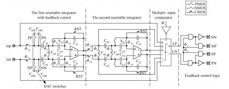
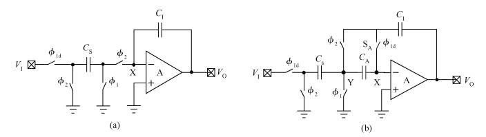
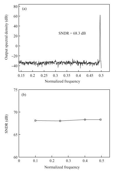
Table 1. Performance comparison of recent incremental ADCs

|
| [1] |
Harrison R R, Watkins P T, Kier R J, et al. A low-power integrated circuit for a wireless 100-electrode neural recording system. IEEE J Solid-State Circuits, 2007, 42(1):123 doi: 10.1109/JSSC.2006.886567
|
| [2] |
Zou X, Xu X, Yao L, et al. A 1-V 450-nW fully integrated programmable biomedical sensor interface chip. IEEE J Solid-State Circuits, 2009, 44(4):1067 doi: 10.1109/JSSC.2009.2014707
|
| [3] |
Chang Y K, Wang C S, Wang C K. A 8-bit 500-KS/s low power SAR ADC for bio-medical applications. IEEE Asian Solid-State Circuits Conference (ASSCC), 2007:228
|
| [4] |
Chen C H, Crop J, Chae J, et al. A 12-bit 7μW/channel 1 kHz/channel incremental ADC for biosensor interface circuits. IEEE Int Symp Circuits and Systems (ISCAS), 2012:2969
|
| [5] |
Yu W, Aslan M, Gabor C T. 82 dB SNDR 20-channel incremental ADC with optimal decimation filter and digital correction. IEEE Custom Integrated Circuits Conference (CICC), 2010:1
|
| [6] |
Gabor C T, Wang Y, Yu W H, et al. Incremental data converters. Proceedings of the 19th International Symposium on Mathematical Theory of Networks and Systems-MTNS, 2010, 5(9):715
|
| [7] |
Liang J, Johns D A. A frequency-scalable 15-bit incremental ADC for low power sensor applications. IEEE Int Symp Circuits Syst (ISCAS), 2010:2418
|
| [8] |
Liu Y T, Chen J, Chen M. An ultra low power dissipation inverter-based incremental sigma-delta ADC. Procedia Engineering 29, 2012:2050
|
| [9] |
Robert J, Valencic V. Offset and charge injection compensation in an incremental analog-to-digital converter. European Solid-State Circuits Conf, Toulouse, France, 1985: 45
|
| [10] |
Márkus J, Silva J, Gabor C T. Theory and applications of incremental delta-sigma converters. IEEE Trans Circuits Syst I, Regular Papers, 2004, 51(4):678 doi: 10.1109/TCSI.2004.826202
|
| [11] |
Hein S, Ibraham K, Zakhor A. New properties of sigma-delta modulators with DC inputs. IEEE Trans Commun, 1992, 40(8):1375 doi: 10.1109/26.156642
|
| [12] |
Kavusi S, Kakavand H, Gamal A E. On incremental sigma delta modulation with optimal filtering. IEEE Trans Circuits Syst I, Regular Papers, 2007, 53(5):1004
|
| [13] |
Steensgaard J, Zhang Z, Yu W, et al. Noise-power optimization of incremental data converters. IEEE Trans Circuits Syst I, Regular Papers, 2008, 55(5):1289 doi: 10.1109/TCSI.2008.916676
|
| [14] |
Garcia J, Rodriguez S, Rusu A. A low-power CT incremental 3rd order sigma-delta ADC for biosensor applications. IEEE Trans Circuits Syst I, Regular Papers, 2013, 60(1):25 doi: 10.1109/TCSI.2012.2215753
|
| [15] |
Silva J, Moon U K, Steensgaard J, et al. A wideband low-distortion delta-sigma ADC topology. Electron Lett, 2001, 37(12):737 doi: 10.1049/el:20010542
|
| [16] |
Schreier R, Silva J, Steensgaard J, et al. Design-oriented estimation of thermal noise in switched-capacitor circuits. IEEE Trans Circuits Syst I, 2005, 52(11):2358 doi: 10.1109/TCSI.2005.853909
|
| [17] |
Hirokazu Y, Gabor C T. Switched-capacitor track-and-hold amplifiers with low sensitivity to op-amp imperfections. IEEE Trans Circuits Syst I, Regular Papers, 2007, 54(1):193 doi: 10.1109/TCSI.2006.887454
|
| [18] |
Chae Y, Han G. Low voltage, low power, inverter-based switched capacitor delta-sigma modulator. IEEE J Solid-State Circuits, 2009, 44(2):458 doi: 10.1109/JSSC.2008.2010973
|
| [19] |
Yao L. Low-power low-voltage sigma-delta A/D converters in deep-submicron CMOS. PhD Dissertation, Katholieke Universiteit Leuven, Belgium, 2005
|
| [20] |
Zhang J, Lian Y, Yao L. A 0.6-V 82-dB 28.6-μW continuous-time audio delta-sigma modulator. IEEE J Solid-State Circuits, 2011, 46(10):2326 doi: 10.1109/JSSC.2011.2161212
|


Article views: 4161 Times PDF downloads: 84 Times Cited by: 0 Times
Received: 10 March 2014 Revised: 05 May 2014 Online: Published: 01 November 2014
| Citation: |
Ting Huang, Lele Jin, Hui Li, Shengxi Diao, Guoxing Wang, Libin Yao, Lin He. A 1.2 V 600 nW 12-bit 2 kS/s incremental ADC for biosensor application[J]. Journal of Semiconductors, 2014, 35(11): 115007. doi: 10.1088/1674-4926/35/11/115007
****
T Huang, L L Jin, H Li, S X Diao, G X Wang, L B Yao, L He. A 1.2 V 600 nW 12-bit 2 kS/s incremental ADC for biosensor application[J]. J. Semicond., 2014, 35(11): 115007. doi: 10.1088/1674-4926/35/11/115007.

|
| [1] |
Harrison R R, Watkins P T, Kier R J, et al. A low-power integrated circuit for a wireless 100-electrode neural recording system. IEEE J Solid-State Circuits, 2007, 42(1):123 doi: 10.1109/JSSC.2006.886567
|
| [2] |
Zou X, Xu X, Yao L, et al. A 1-V 450-nW fully integrated programmable biomedical sensor interface chip. IEEE J Solid-State Circuits, 2009, 44(4):1067 doi: 10.1109/JSSC.2009.2014707
|
| [3] |
Chang Y K, Wang C S, Wang C K. A 8-bit 500-KS/s low power SAR ADC for bio-medical applications. IEEE Asian Solid-State Circuits Conference (ASSCC), 2007:228
|
| [4] |
Chen C H, Crop J, Chae J, et al. A 12-bit 7μW/channel 1 kHz/channel incremental ADC for biosensor interface circuits. IEEE Int Symp Circuits and Systems (ISCAS), 2012:2969
|
| [5] |
Yu W, Aslan M, Gabor C T. 82 dB SNDR 20-channel incremental ADC with optimal decimation filter and digital correction. IEEE Custom Integrated Circuits Conference (CICC), 2010:1
|
| [6] |
Gabor C T, Wang Y, Yu W H, et al. Incremental data converters. Proceedings of the 19th International Symposium on Mathematical Theory of Networks and Systems-MTNS, 2010, 5(9):715
|
| [7] |
Liang J, Johns D A. A frequency-scalable 15-bit incremental ADC for low power sensor applications. IEEE Int Symp Circuits Syst (ISCAS), 2010:2418
|
| [8] |
Liu Y T, Chen J, Chen M. An ultra low power dissipation inverter-based incremental sigma-delta ADC. Procedia Engineering 29, 2012:2050
|
| [9] |
Robert J, Valencic V. Offset and charge injection compensation in an incremental analog-to-digital converter. European Solid-State Circuits Conf, Toulouse, France, 1985: 45
|
| [10] |
Márkus J, Silva J, Gabor C T. Theory and applications of incremental delta-sigma converters. IEEE Trans Circuits Syst I, Regular Papers, 2004, 51(4):678 doi: 10.1109/TCSI.2004.826202
|
| [11] |
Hein S, Ibraham K, Zakhor A. New properties of sigma-delta modulators with DC inputs. IEEE Trans Commun, 1992, 40(8):1375 doi: 10.1109/26.156642
|
| [12] |
Kavusi S, Kakavand H, Gamal A E. On incremental sigma delta modulation with optimal filtering. IEEE Trans Circuits Syst I, Regular Papers, 2007, 53(5):1004
|
| [13] |
Steensgaard J, Zhang Z, Yu W, et al. Noise-power optimization of incremental data converters. IEEE Trans Circuits Syst I, Regular Papers, 2008, 55(5):1289 doi: 10.1109/TCSI.2008.916676
|
| [14] |
Garcia J, Rodriguez S, Rusu A. A low-power CT incremental 3rd order sigma-delta ADC for biosensor applications. IEEE Trans Circuits Syst I, Regular Papers, 2013, 60(1):25 doi: 10.1109/TCSI.2012.2215753
|
| [15] |
Silva J, Moon U K, Steensgaard J, et al. A wideband low-distortion delta-sigma ADC topology. Electron Lett, 2001, 37(12):737 doi: 10.1049/el:20010542
|
| [16] |
Schreier R, Silva J, Steensgaard J, et al. Design-oriented estimation of thermal noise in switched-capacitor circuits. IEEE Trans Circuits Syst I, 2005, 52(11):2358 doi: 10.1109/TCSI.2005.853909
|
| [17] |
Hirokazu Y, Gabor C T. Switched-capacitor track-and-hold amplifiers with low sensitivity to op-amp imperfections. IEEE Trans Circuits Syst I, Regular Papers, 2007, 54(1):193 doi: 10.1109/TCSI.2006.887454
|
| [18] |
Chae Y, Han G. Low voltage, low power, inverter-based switched capacitor delta-sigma modulator. IEEE J Solid-State Circuits, 2009, 44(2):458 doi: 10.1109/JSSC.2008.2010973
|
| [19] |
Yao L. Low-power low-voltage sigma-delta A/D converters in deep-submicron CMOS. PhD Dissertation, Katholieke Universiteit Leuven, Belgium, 2005
|
| [20] |
Zhang J, Lian Y, Yao L. A 0.6-V 82-dB 28.6-μW continuous-time audio delta-sigma modulator. IEEE J Solid-State Circuits, 2011, 46(10):2326 doi: 10.1109/JSSC.2011.2161212
|

 WeChat ID
Journal of Semiconductors © 2017 All Rights Reserved 京ICP备05085259号-2

 DownLoad: