1. Institute of Photo-Electronic Thin Film Devices and Technology, Nankai University, Tianjin 300071, ChinaInstitute of Photo-Electronic Thin Film Devices and Technology, Nankai University, Tianjin 300071, China
2. Tianjin Key Laboratory of Photo-Electronic Thin Film Devices and Technology, Nankai University, Tianjin 300071, ChinaTianjin Key Laboratory of Photo-Electronic Thin Film Devices and Technology, Nankai University, Tianjin 300071, China
3. Key Laboratory of Opto-Electronic Information Science and Technology for Ministry of Education, Nankai University, Tianjin 300071, ChinaKey Laboratory of Opto-Electronic Information Science and Technology for Ministry of Education, Nankai University, Tianjin 300071, China
Abstract: Modified textured surface boron-doped ZnO (ZnO:B) transparent conductive layers for thin-film solar cells were fabricated by low-pressure metal organic chemical vapor deposition (LP-MOCVD) on glass substrates. These modified textured surface ZnO:B thin films included two layers. The first ZnO:B layer, which has a pyramid-shaped texture, was deposited under conventional growth conditions, and the second layer, which has a sphere-like structure, at a relatively lower growth temperature. Typical bi-layer ZnO:B thin films exhibit a high electron mobility of 27.6 cm2/(V· s) due to improved grain boundary states. For bi-layer ZnO:B, the haze value increases and the total transmittance decreases with the increasing film thickness of the second modification layer. When applied in hydrogenated microcrystalline silicon (μc-Si:H) thin-film solar cells, the modified textured surface ZnO:B layers present relatively higher conversion efficiency than conventional ZnO:B films.
Silicon (Si)-based thin-film solar cells have strong potential for energy mass production and are based on low usage of abundant and non-toxic materials[1,2]. Compared to hydrogenated amorphous silicon (a-Si:H), microcrystalline silicon ($\mu $c-Si:H) solar cells with a narrow band gap ($E_{\rm g}$$\approx $ 1.1 eV) have a broader spectral response and higher photocurrent[3-5]. However, the absorption coefficient of $\mu $c-Si:H is natively low within the near infrared (NIR) region. An advanced light-trapping structure is essential to eliminate optical losses and to capture solar radiation effectively for $\mu $c-Si:H solar cells[6-9]. An efficient approach to improve the light trapping ability of solar cells is texturing transparent conductive oxide (TCO) layers applied as front electrodes in which the incident light is scattered. Rough textured surface zinc oxide (ZnO) thin films are widely used as light-scattering layers in superstrate-type (p-i-n) Si-based thin-film solar cells[10-12. Magnetron sputtering and metal organic chemical vapor deposition (MOCVD) are the two main fabrication techniques used to deposit textured surface ZnO-TCO layers for Si-based thin-film solar cells[13-15]. The MOCVD of ZnO-TCO can directly create rough pyramid-like crystal grains with excellent light-scattering capabilities. In addition, MOCVD-ZnO thin films have been shown to be successfully integrated into Si-based thin-film solar cells with excellent performance[16-19].
Boron-doped ZnO (ZnO:B) thin films grown by MOCVD have typical resistivity values as low as $\sim $1.0-3.0 $\times $ 10$^{-3}$$\Omega $$\cdot $cm and large pyramid-like crystal grains. There are several factors concerning ZnO:B-TCO layers to be considered in solar cells. On the one hand, the introduction of extrinsic boron dopants will result in higher free carrier absorption in the NIR range. And on the other, some researchers have reported that the substrate morphology strongly influences the growth and performance of $\mu $c-Si:H solar cells: a rougher substrate generally allows for enhanced light scattering within the device and thus, for a gain in photocurrent; however, the open-circuit voltage ($V_{\rm oc})$ and fill factor (FF) are usually both reduced due to many defects existing in the intrinsic $\mu $c-Si:H (i.e. absorbing layer) and interface layers. Therefore, appropriate surface morphology should be considered when these rough ZnO:B thin films are applied in $\mu $c-Si:H solar cells. The IMT group suggested that the surface morphology was modified by applying a plasma treatment on the ZnO layers, which leads to the growth of dense $\mu $c-Si:H and reduces the crack density in solar-cell devices[17]. Accordingly, there should be a trade-off between sheet resistance and optical transmittance, and the surface structure for ZnO:B TCO layers in $\mu $c-Si:H solar cells.
In this work, we propose a modified bi-layer textured surface ZnO:B TCO thin film for $\mu $c-Si:H solar cells grown using the MOCVD technique. The structural, electrical and optical properties of ZnO:B TCO thin films for $\mu $c-Si:H solar cells are all investigated.
2.
Experimental details
In this experiment, conventional single-layer and bi-layer ZnO:B thin films were deposited by MOCVD on 2 mm thick glass substrates, 10 $\times$ 10 cm$^{2}$ in size. Diethylzinc (DEZn) and the water vapors carried by purified Ar gas (purity: 99.999%) were used as the reactant gases, and their temperatures kept at 318 and 333 K, respectively. Diborane (B$_{2}$H$_{6})$, 1.0% diluted in hydrogen, was used as the doping gas. These vapors and the B$_{2}$H$_{6}$ gas were separately introduced into the reactor through an upward shower, and there were no pre-reactions in it. The distance between the shower and substrate was 50 mm and the working pressure was 133.3 Pa. The flow rate of B$_{2}$H$_{6}$ was set at 3.0 sccm for all the ZnO:B thin films. For the bi-layer ZnO thin films, the first ZnO:B thin film, with a pyramid-like, rough textured surface acting as the main light-scattering layer, was deposited at 423 K for 30 min, and the second ZnO:B thin films, with sphere-like grain structures acting as the modification layer, were deposited at 398 K for 5, 10 and 15 min, respectively. For comparison, a conventional single-layer ZnO:B was used as the reference sample.
The film thicknesses were measured with a step profilometer (AMBIOS-XP2), and the surface morphology and root-mean-square (RMS) roughness of the ZnO films were characterized via scanning electron microscopy (FE-SEM, ZEISS Supra-550p) using a 30.0 kV operating voltage and atom force microscopy (AFM/Seiko SPA 400) using the same pyramidal Si$_{3}$N$_{4}$ tip in contact mode, respectively. The carrier concentrations, sheet resistances and electron mobilities were determined by Hall measurement (Accent HL5500 PC) using the van der Pauw configuration. The optical transmittances, including the specular and total, were recorded using a double-beam spectrometer with an integrating sphere (UV-vis-NIR spectrometer/Varian Cary 5000). The haze ration was calculated as Haze $=$ Diffuse $T$ (DT)/Total $T$ (TT) (Total $T$ (TT) $=$ (Diffuse $T$ (DT) $+$ Specular $T$ (ST)) $\times $ 100%), where $T$ is the transmittance.
P-i-i n $\mu $c-Si:H thin-film solar cells were deposited on the ZnO-coated glass substrates by plasma-enhanced chemical vapor deposition (PECVD) in a cluster-tool system working at a very high excitation frequency (VHF). The solar cells were then patterned to an area of 0.25 cm$^{2}$. The performance of the solar cells was characterized by quantum efficiency (QE) and current-voltage ($I$-$V)$ measurements under 1 sun (AM 1.5, 100 mW/cm$^{2})$ illumination, and included the open-circuit voltage ($V_{\rm oc})$, fill factor (FF), short-circuit current density ($J_{\rm sc})$, and efficiency.
3.
Results and discussion
3.1
Structural properties
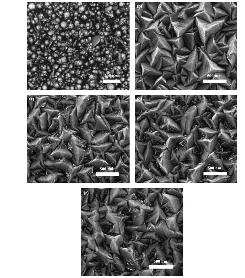
Typical SEM images of the surface morphology of the conventional single-layer and bi-layer ZnO:B thin films are shown in Figs. 1(a)-1(e). The MOCVD-grown ZnO:B thin film grown at 398 K presents a relatively plane structure with the (002) crystallographic orientation perpendicular to the substrate, as shown in Fig. 1(a). In this case, the ZnO:B thin film contains some sphere-like grains and gives a smooth structure. However, the MOCVD-grown ZnO:B thin film grown at 423 K exhibits a rough textured surface with the (110) crystallographic orientation perpendicular to the substrate, as shown in Fig. 1(b). The above phenomenon can be attributed to the different surface-free energies, and hence the substrate temperature activates the ZnO film growth from a relatively lower surface free energy to a higher surface free energy (1.6 J/m$^{2}$ for (002) and 2.0 J/m$^{2}$ for (110), respectively)[16,20]. The samples in Figs. 1(c)-1(e) are bi-layer ZnO:B thin films, i.e. conventional rough textured surface ZnO:B layers covered with 5, 10 and 15 min thickness ZnO:B thin films grown at 398 K, respectively. From the SEM images of the bi-layer ZnO:B thin films, one can see that the boundary sites between the large pyramid-like grains are filled with small sphere-like grains. In addition, the sharp textured surface ZnO:B thin films become more "gentle". It can be speculated that these relatively "gentle" surfaces will contribute to the subsequent growth of the $\mu $c-Si:H thin films. Furthermore, these bi-layer ZnO:B thin films can be accomplished in the MOCVD deposition system through adjustment of the substrate temperature.
Figure
1.
Typical SEM images of MOCVD-ZnO:B thin films. (a) A smooth surface ZnO:B at $T$$=$ 298 K and $t$$=$ 30 min. (b) A rough textured surface ZnO:B at $T$$=$ 423 K and $t$$=$ 30 min. (c)-(e) A bi-layer structure, i.e. a conventional rough textured surface ZnO:B covered with a 5, 10 and 15 min thickness modification layer, respectively.
Table 1 gives the electrical properties of the MOCVD-grown ZnO:B thin films. For polycrystalline ZnO thin films, the charge carrier transport through the layer is known to be limited mainly by two phenomena: scattering at ionized impurities within the grains (bulk scattering) and scattering at the grain boundaries[8]. By depositing bi-layer ZnO:B thin films instead of conventional mono-layers, the main intentions are to reserve large grains while maintaining a certain sheet resistance.
Table
1.
The electrical properties of the MOCVD-ZnO:B thin films.
From Table 1, a relatively high electron mobility of 27.6 cm$^{2}$/(V$\cdot $s) was obtained with a 10 min thickness modification layer. The improved electron mobility for bi-layer ZnO:B can be attributed to the reduction in the quantity of the small grains between the large pyramid-like grains[21]. Bi-layer ZnO:B with a 10 min thickness modification layer also presents a low sheet resistance of 14.1 $\Omega $. However, bi-layer ZnO:B with a 15 min thickness modification layer gives the lowest electron mobility of 15.6 cm$^{2}$/(V$\cdot $s), resulting from the higher amount of boundary defects between the sphere-like grains. It is well known that the MOCVD ZnO:B thin films deposited at 398 K exhibit low electron mobility due to small sphere-like grains[16]. Therefore, an appropriate modification layer is important for bi-layer ZnO:B.
The optical transmittances and haze curves of the ZnO:B thin films are shown in Figs. 2(a)-2(b). The conventional textured surface ZnO:B thin film shows high total transmittances (TT) and high haze values in the range 400-1100 nm, resulting from its thinner film thickness and larger grain size. For bi-layer ZnO:B, the haze value increases and the TT decreases with the increasing film thickness of the modification layer.
Figure
2.
The typical optical transmittances and haze curves of the MOCVD-ZnO:B thin films. $a$: A smooth surface ZnO:B at $T$$=$ 298 K and $t$$=$ 30 min. $b$: A rough textured surface ZnO:B at $T$$=$ 423 K and $t$$=$ 30 min. $c$-$e$: A bi-layer structure, i.e. a conventional rough textured surface ZnO:B covered with a 5, 10 and 15 min thickness modification layer, respectively.
3.3
The application of bi-layer ZnO:B in $\boldsymbol{\mu}$c-Si:H solar cells
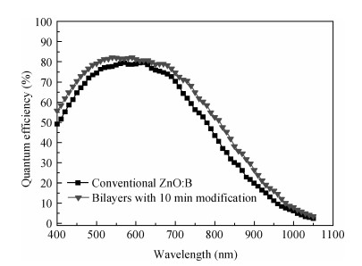
As was shown above, a bi-layer ZnO:B with a textured structure, low sheet resistance and high transparency can be obtained with a 10 min thickness modification layer. For comparison, the conventional ZnO:B and bi-layer ZnO:B thin films were applied in $\mu $c-Si:H solar cells, as seen in Fig. 3. The $\mu $c-Si:H solar cell with a conventional ZnO:B layer exhibits an efficiency of 5.20% with $J_{\rm SC}$$=$ 22.89 mA/cm$^{2}$, $V_{\rm OC}$$=$ 0.43 V and FF $=$ 53.1%, and the $\mu $c-Si:H solar cell with a bi-layer ZnO:B presents a relatively higher efficiency of 5.59% ($J_{\rm SC}$$=$ 24.69 mA/cm$^{2}$, $V_{\rm OC}$$=$ 0.44 V and FF $=$ 51.2%). The bi-layer ZnO:B effectively improved the $J_{\rm SC}$ and $V_{\rm OC}$, but the FF decreased due to a relatively higher series resistance $R_{\rm series}$. Figure 4 shows the QE curves of the $\mu $c-Si:H solar cells with conventional ZnO:B and bi-layer ZnO:B thin films. It can be clearly seen that the bi-layer ZnO:B thin film effectively increases the spectral response of the sunlight in the wavelength range 400 to 1000 nm. This increased light absorption in the $\mu $c-Si:H intrinsic layer leads to a higher $J_{\rm SC}$. Though the bi-layer ZnO:B film has a lower haze value than the conventional mono-layer sample, it can effectively reduce the defects existing in intrinsic $\mu $c-Si:H (i.e. absorbing layer, i layer) and interface layers[17]. Sharp pyramid grains will result in cracks during the microcrystalline growth process, and such cracks often start off in the valleys of an underlying rough substrate. For this kind of $\mu $c-Si:H phase, one can expect a large amount of structural defects, which can be active either as carrier traps or recombination centers. They can lead to low values of shunt resistance, $R_{\rm shunt}$, but can also result in high values of the diode's reverse saturation current density and thus reduce the efficiency of the whole solar cell[22]. Additionally, the sharp pyramid grains may influence the growth quality of the p-layer and thus deteriorate the performance of the p-n junction. Therefore, "gentle" bi-layer ZnO:B thin films are helpful to the growth of subsequent $\mu $c-Si:H layers and thus improve the quality of the $\mu $c-Si:H layers and the efficiency of the solar cells.
Figure
3.
Current-voltage curves of $\mu $c-Si:H thin-film solar cells on conventional textured surface ZnO:B and bi-layer ZnO:B.
In summary, modified bi-layer textured surface boron-doped ZnO (ZnO:B) transparent conductive layers for thin-film solar cells were fabricated by low-pressure metal organic chemical vapor deposition (LP-MOCVD) on glass substrates. Typical bi-layer ZnO:B thin films exhibit a compound textured surface and a high electron mobility of 27.6 cm$^{2}$/(V$\cdot$s) due to improved grain boundary states. The bi-layer textured surface ZnO:B presents a relatively higher conversion efficiency compared to conventional ZnO:B. These modified bi-layer textured surface ZnO:B films are helpful to the growth of subsequent $\mu $c-Si:H layers and improve the quality of the $\mu $c-Si:H absorbing layers.
References
[1]
Shah A V, Schade H, Vanecek M, et al. Thin-film silicon solar cell technology. Prog Photovolt:Res and Appl, 2004, 12:113 doi: 10.1002/(ISSN)1099-159X
[2]
Hoffmann W, Pellkofer T. Thin films in photovoltaics:technologies and perspectives. Thin Solid Films, 2012, 520:4094 doi: 10.1016/j.tsf.2011.04.146
[3]
Hsu C M, Battaglia C, Pahud C, et al. High-efficiency amorphous silicon solar cell on a periodic nanocone back reflector. Adv Energy Mater, 2012, 2:628 doi: 10.1002/aenm.201100514
[4]
Müller J, Rech B, Springer J, et al. TCO and light trapping in silicon thin film solar cells. Sol Energy, 2004, 77:917 doi: 10.1016/j.solener.2004.03.015
[5]
Yan B, Yue G, Sivec L, et al. Innovative dual function nc-SiOx:H layer leading to a > 16% efficient multi-junction thin-film silicon solar cell. Appl Phys Lett, 2011, 99:113512 doi: 10.1063/1.3638068
[6]
Janthong B, Hongsingthong A, Krajangsang T, et al. Novel a-Si:H/μc-Si:H tandem cell with lower optical loss. J Non-Cryst Solids. 2012, 358:2478 doi: 10.1016/j.jnoncrysol.2012.01.060
[7]
Ruske F, Jacobs C, Sittinger V, et al. Large area ZnO:Al films with tailored light scattering properties for photovoltaic applications. Thin Solid Films, 2007, 515:8695 doi: 10.1016/j.tsf.2007.03.107
[8]
Ding L, Boccard M, Bugnon G, et al. Highly transparent ZnO bilayers by LP-MOCVD as front electrodes for thin-film micromorph silicon solar cells. Sol Energy Mater Sol Cells, 2012, 98:331 doi: 10.1016/j.solmat.2011.11.033
[9]
Bugnon G, Parascandolo G, Söderström T, et al. A new view of microcrystalline silicon:the role of plasma processing in achieving a dense and stable absorber material for photovoltaic applications. Adv Funct Mater, 2012, 22:3665 doi: 10.1002/adfm.v22.17
[10]
Hongsingthong A, Krajangsang T, Fujioka H, et al. Improvement of short-circuit current in silicon-based thin film solar cells using ZnO films with very high haze value. 26th European Photovoltaic Solar Energy Conference and Exhibition, DOI:10.4229/26thEUPVSEC2011-3AV.2.9
[11]
Kluth O, Rech B, Houben L, et al. Texture etched ZnO:Al coated glass substrates for silicon based thin film solar cells. Thin Solid Films, 1999, 351:247 doi: 10.1016/S0040-6090(99)00085-1
[12]
Hongsingthong A, Yunaz I A, Miyajima S, et al. Preparation of ZnO thin films using MOCVD technique with D2O/H2O gas mixture for use as TCO in silicon-based thin film solar cells. Sol Energy MaterSol Cells, 2011, 95:171 doi: 10.1016/j.solmat.2010.04.025
[13]
Chen X L, Li L N, Wang F, et al. Natively textured surface aluminum-doped zinc oxide transparent conductive layers for thin film solar cells via pulsed direct-current reactive magnetron sputtering. Thin Solid Films, 2012, 520:5392 doi: 10.1016/j.tsf.2012.03.120
[14]
Owen J I, Zhang W, Köhl D, et al. Study on the in-line sputtering growth and structural properties of polycrystalline ZnO:Al on ZnO and glass. J Cryst Growth, 2012, 344:12 doi: 10.1016/j.jcrysgro.2012.01.043
[15]
Hüpkes J, Owen J I, Pust S E, et al. Chemical etching of zinc oxide for thin-film silicon solar cells. Chem Phys Phys Chem, 2012, 13:66 doi: 10.1002/cphc.201100738
[16]
Chen X L, Geng X H, Xue J M, et al. Temperature-dependent growth of zinc oxide thin films grown by metal organic chemical vapor deposition. J Cryst Growth, 2006, 296:43 doi: 10.1016/j.jcrysgro.2006.08.028
[17]
Python M, Vallat-Sauvain E, Bailat J, et al. Relation between substrate surface morphology and microcrystalline silicon solar cell performance. J Non-Cryst Solids, 2008, 354:2258 doi: 10.1016/j.jnoncrysol.2007.09.084
[18]
Moriya Y, Krajangsang T, Sichanugrist P, et al. Development of high-efficiency tandem silicon solar cells on W-textured zinc oxide-coated soda-lime glass substrates. Photovoltaic Specialists Conference (PVSC), DOI:10.1109/PVSC.2012.6318219.
Jiang X, Jia C L, Szyszka B. Manufacture of specific structure of aluminum-doped zinc oxide films by patterning the substrate surface. Appl Phys Lett, 2002, 80:3090 doi: 10.1063/1.1473683
[21]
Yan C B, Chen X L, Wang F, et al. Textured surface ZnO:B/(hydrogenated gallium-doped ZnO) and (hydrogenated gallium-doped ZnO)/ZnO:B transparent conductive oxide layers for Si-based thin film solar cells. Thin Solid Films, 2012, 521:249 doi: 10.1016/j.tsf.2011.10.203
[22]
Shah A. Thin-film silicon solar cells. Swiss EPFL Press, 2010
Fig. 1.
Typical SEM images of MOCVD-ZnO:B thin films. (a) A smooth surface ZnO:B at $T$$=$ 298 K and $t$$=$ 30 min. (b) A rough textured surface ZnO:B at $T$$=$ 423 K and $t$$=$ 30 min. (c)-(e) A bi-layer structure, i.e. a conventional rough textured surface ZnO:B covered with a 5, 10 and 15 min thickness modification layer, respectively.
Fig. 2.
The typical optical transmittances and haze curves of the MOCVD-ZnO:B thin films. $a$: A smooth surface ZnO:B at $T$$=$ 298 K and $t$$=$ 30 min. $b$: A rough textured surface ZnO:B at $T$$=$ 423 K and $t$$=$ 30 min. $c$-$e$: A bi-layer structure, i.e. a conventional rough textured surface ZnO:B covered with a 5, 10 and 15 min thickness modification layer, respectively.
Table 1.
The electrical properties of the MOCVD-ZnO:B thin films.
[1]
Shah A V, Schade H, Vanecek M, et al. Thin-film silicon solar cell technology. Prog Photovolt:Res and Appl, 2004, 12:113 doi: 10.1002/(ISSN)1099-159X
[2]
Hoffmann W, Pellkofer T. Thin films in photovoltaics:technologies and perspectives. Thin Solid Films, 2012, 520:4094 doi: 10.1016/j.tsf.2011.04.146
[3]
Hsu C M, Battaglia C, Pahud C, et al. High-efficiency amorphous silicon solar cell on a periodic nanocone back reflector. Adv Energy Mater, 2012, 2:628 doi: 10.1002/aenm.201100514
[4]
Müller J, Rech B, Springer J, et al. TCO and light trapping in silicon thin film solar cells. Sol Energy, 2004, 77:917 doi: 10.1016/j.solener.2004.03.015
[5]
Yan B, Yue G, Sivec L, et al. Innovative dual function nc-SiOx:H layer leading to a > 16% efficient multi-junction thin-film silicon solar cell. Appl Phys Lett, 2011, 99:113512 doi: 10.1063/1.3638068
[6]
Janthong B, Hongsingthong A, Krajangsang T, et al. Novel a-Si:H/μc-Si:H tandem cell with lower optical loss. J Non-Cryst Solids. 2012, 358:2478 doi: 10.1016/j.jnoncrysol.2012.01.060
[7]
Ruske F, Jacobs C, Sittinger V, et al. Large area ZnO:Al films with tailored light scattering properties for photovoltaic applications. Thin Solid Films, 2007, 515:8695 doi: 10.1016/j.tsf.2007.03.107
[8]
Ding L, Boccard M, Bugnon G, et al. Highly transparent ZnO bilayers by LP-MOCVD as front electrodes for thin-film micromorph silicon solar cells. Sol Energy Mater Sol Cells, 2012, 98:331 doi: 10.1016/j.solmat.2011.11.033
[9]
Bugnon G, Parascandolo G, Söderström T, et al. A new view of microcrystalline silicon:the role of plasma processing in achieving a dense and stable absorber material for photovoltaic applications. Adv Funct Mater, 2012, 22:3665 doi: 10.1002/adfm.v22.17
[10]
Hongsingthong A, Krajangsang T, Fujioka H, et al. Improvement of short-circuit current in silicon-based thin film solar cells using ZnO films with very high haze value. 26th European Photovoltaic Solar Energy Conference and Exhibition, DOI:10.4229/26thEUPVSEC2011-3AV.2.9
[11]
Kluth O, Rech B, Houben L, et al. Texture etched ZnO:Al coated glass substrates for silicon based thin film solar cells. Thin Solid Films, 1999, 351:247 doi: 10.1016/S0040-6090(99)00085-1
[12]
Hongsingthong A, Yunaz I A, Miyajima S, et al. Preparation of ZnO thin films using MOCVD technique with D2O/H2O gas mixture for use as TCO in silicon-based thin film solar cells. Sol Energy MaterSol Cells, 2011, 95:171 doi: 10.1016/j.solmat.2010.04.025
[13]
Chen X L, Li L N, Wang F, et al. Natively textured surface aluminum-doped zinc oxide transparent conductive layers for thin film solar cells via pulsed direct-current reactive magnetron sputtering. Thin Solid Films, 2012, 520:5392 doi: 10.1016/j.tsf.2012.03.120
[14]
Owen J I, Zhang W, Köhl D, et al. Study on the in-line sputtering growth and structural properties of polycrystalline ZnO:Al on ZnO and glass. J Cryst Growth, 2012, 344:12 doi: 10.1016/j.jcrysgro.2012.01.043
[15]
Hüpkes J, Owen J I, Pust S E, et al. Chemical etching of zinc oxide for thin-film silicon solar cells. Chem Phys Phys Chem, 2012, 13:66 doi: 10.1002/cphc.201100738
[16]
Chen X L, Geng X H, Xue J M, et al. Temperature-dependent growth of zinc oxide thin films grown by metal organic chemical vapor deposition. J Cryst Growth, 2006, 296:43 doi: 10.1016/j.jcrysgro.2006.08.028
[17]
Python M, Vallat-Sauvain E, Bailat J, et al. Relation between substrate surface morphology and microcrystalline silicon solar cell performance. J Non-Cryst Solids, 2008, 354:2258 doi: 10.1016/j.jnoncrysol.2007.09.084
[18]
Moriya Y, Krajangsang T, Sichanugrist P, et al. Development of high-efficiency tandem silicon solar cells on W-textured zinc oxide-coated soda-lime glass substrates. Photovoltaic Specialists Conference (PVSC), DOI:10.1109/PVSC.2012.6318219.
Jiang X, Jia C L, Szyszka B. Manufacture of specific structure of aluminum-doped zinc oxide films by patterning the substrate surface. Appl Phys Lett, 2002, 80:3090 doi: 10.1063/1.1473683
[21]
Yan C B, Chen X L, Wang F, et al. Textured surface ZnO:B/(hydrogenated gallium-doped ZnO) and (hydrogenated gallium-doped ZnO)/ZnO:B transparent conductive oxide layers for Si-based thin film solar cells. Thin Solid Films, 2012, 521:249 doi: 10.1016/j.tsf.2011.10.203
[22]
Shah A. Thin-film silicon solar cells. Swiss EPFL Press, 2010
X L Chen, C B Yan, X H Geng, D K Zhang, C C Wei, Y Zhao, X D Zhang. Modified textured surface MOCVD-ZnO:B transparent conductive layers for thin-film solar cells[J]. J. Semicond., 2014, 35(4): 043002. doi: 10.1088/1674-4926/35/4/043002.
Export: BibTexEndNote
Share:
Article Metrics
Article views: 2523 TimesPDF downloads: 9 TimesCited by: 0 Times
History
Received: 21 September 2013Revised: 20 November 2013Online:Published: 01 April 2014
Xinliang Chen, Congbo Yan, Xinhua Geng, Dekun Zhang, Changchun Wei, Ying Zhao, Xiaodan Zhang. Modified textured surface MOCVD-ZnO:B transparent conductive layers for thin-film solar cells[J]. Journal of Semiconductors, 2014, 35(4): 043002. doi: 10.1088/1674-4926/35/4/043002 ****X L Chen, C B Yan, X H Geng, D K Zhang, C C Wei, Y Zhao, X D Zhang. Modified textured surface MOCVD-ZnO:B transparent conductive layers for thin-film solar cells[J]. J. Semicond., 2014, 35(4): 043002. doi: 10.1088/1674-4926/35/4/043002.
X L Chen, C B Yan, X H Geng, D K Zhang, C C Wei, Y Zhao, X D Zhang. Modified textured surface MOCVD-ZnO:B transparent conductive layers for thin-film solar cells[J]. J. Semicond., 2014, 35(4): 043002. doi: 10.1088/1674-4926/35/4/043002.
Institute of Photo-Electronic Thin Film Devices and Technology, Nankai University, Tianjin 300071, China
2.
Tianjin Key Laboratory of Photo-Electronic Thin Film Devices and Technology, Nankai University, Tianjin 300071, China
3.
Key Laboratory of Opto-Electronic Information Science and Technology for Ministry of Education, Nankai University, Tianjin 300071, China
Funds:
the Fundamental Research Funds for the Central Universities, China65010341
the Tianjin Applied Basic Research Project and Cutting-Edge Technology Research Plan, China13JCZDJC26900
the State Key Development Program for Basic Research of China2011CBA00705
the State Key Development Program for Basic Research of China2011CBA00707
the Tianjin Major Science and Technology Support Project, China11TXSYGX22100
Project supported by the State Key Development Program for Basic Research of China (Nos. 2011CBA00705, 2011CBA00706, 2011CBA00707), the Tianjin Applied Basic Research Project and Cutting-Edge Technology Research Plan, China (No. 13JCZDJC26900), the Tianjin Major Science and Technology Support Project, China (No. 11TXSYGX22100), and the Fundamental Research Funds for the Central Universities, China (No. 65010341)
the State Key Development Program for Basic Research of China2011CBA00706
Modified textured surface boron-doped ZnO (ZnO:B) transparent conductive layers for thin-film solar cells were fabricated by low-pressure metal organic chemical vapor deposition (LP-MOCVD) on glass substrates. These modified textured surface ZnO:B thin films included two layers. The first ZnO:B layer, which has a pyramid-shaped texture, was deposited under conventional growth conditions, and the second layer, which has a sphere-like structure, at a relatively lower growth temperature. Typical bi-layer ZnO:B thin films exhibit a high electron mobility of 27.6 cm2/(V· s) due to improved grain boundary states. For bi-layer ZnO:B, the haze value increases and the total transmittance decreases with the increasing film thickness of the second modification layer. When applied in hydrogenated microcrystalline silicon (μc-Si:H) thin-film solar cells, the modified textured surface ZnO:B layers present relatively higher conversion efficiency than conventional ZnO:B films.
Silicon (Si)-based thin-film solar cells have strong potential for energy mass production and are based on low usage of abundant and non-toxic materials[1,2]. Compared to hydrogenated amorphous silicon (a-Si:H), microcrystalline silicon ($\mu $c-Si:H) solar cells with a narrow band gap ($E_{\rm g}$$\approx $ 1.1 eV) have a broader spectral response and higher photocurrent[3-5]. However, the absorption coefficient of $\mu $c-Si:H is natively low within the near infrared (NIR) region. An advanced light-trapping structure is essential to eliminate optical losses and to capture solar radiation effectively for $\mu $c-Si:H solar cells[6-9]. An efficient approach to improve the light trapping ability of solar cells is texturing transparent conductive oxide (TCO) layers applied as front electrodes in which the incident light is scattered. Rough textured surface zinc oxide (ZnO) thin films are widely used as light-scattering layers in superstrate-type (p-i-n) Si-based thin-film solar cells[10-12. Magnetron sputtering and metal organic chemical vapor deposition (MOCVD) are the two main fabrication techniques used to deposit textured surface ZnO-TCO layers for Si-based thin-film solar cells[13-15]. The MOCVD of ZnO-TCO can directly create rough pyramid-like crystal grains with excellent light-scattering capabilities. In addition, MOCVD-ZnO thin films have been shown to be successfully integrated into Si-based thin-film solar cells with excellent performance[16-19].
Boron-doped ZnO (ZnO:B) thin films grown by MOCVD have typical resistivity values as low as $\sim $1.0-3.0 $\times $ 10$^{-3}$$\Omega $$\cdot $cm and large pyramid-like crystal grains. There are several factors concerning ZnO:B-TCO layers to be considered in solar cells. On the one hand, the introduction of extrinsic boron dopants will result in higher free carrier absorption in the NIR range. And on the other, some researchers have reported that the substrate morphology strongly influences the growth and performance of $\mu $c-Si:H solar cells: a rougher substrate generally allows for enhanced light scattering within the device and thus, for a gain in photocurrent; however, the open-circuit voltage ($V_{\rm oc})$ and fill factor (FF) are usually both reduced due to many defects existing in the intrinsic $\mu $c-Si:H (i.e. absorbing layer) and interface layers. Therefore, appropriate surface morphology should be considered when these rough ZnO:B thin films are applied in $\mu $c-Si:H solar cells. The IMT group suggested that the surface morphology was modified by applying a plasma treatment on the ZnO layers, which leads to the growth of dense $\mu $c-Si:H and reduces the crack density in solar-cell devices[17]. Accordingly, there should be a trade-off between sheet resistance and optical transmittance, and the surface structure for ZnO:B TCO layers in $\mu $c-Si:H solar cells.
In this work, we propose a modified bi-layer textured surface ZnO:B TCO thin film for $\mu $c-Si:H solar cells grown using the MOCVD technique. The structural, electrical and optical properties of ZnO:B TCO thin films for $\mu $c-Si:H solar cells are all investigated.
2.
Experimental details
In this experiment, conventional single-layer and bi-layer ZnO:B thin films were deposited by MOCVD on 2 mm thick glass substrates, 10 $\times$ 10 cm$^{2}$ in size. Diethylzinc (DEZn) and the water vapors carried by purified Ar gas (purity: 99.999%) were used as the reactant gases, and their temperatures kept at 318 and 333 K, respectively. Diborane (B$_{2}$H$_{6})$, 1.0% diluted in hydrogen, was used as the doping gas. These vapors and the B$_{2}$H$_{6}$ gas were separately introduced into the reactor through an upward shower, and there were no pre-reactions in it. The distance between the shower and substrate was 50 mm and the working pressure was 133.3 Pa. The flow rate of B$_{2}$H$_{6}$ was set at 3.0 sccm for all the ZnO:B thin films. For the bi-layer ZnO thin films, the first ZnO:B thin film, with a pyramid-like, rough textured surface acting as the main light-scattering layer, was deposited at 423 K for 30 min, and the second ZnO:B thin films, with sphere-like grain structures acting as the modification layer, were deposited at 398 K for 5, 10 and 15 min, respectively. For comparison, a conventional single-layer ZnO:B was used as the reference sample.
The film thicknesses were measured with a step profilometer (AMBIOS-XP2), and the surface morphology and root-mean-square (RMS) roughness of the ZnO films were characterized via scanning electron microscopy (FE-SEM, ZEISS Supra-550p) using a 30.0 kV operating voltage and atom force microscopy (AFM/Seiko SPA 400) using the same pyramidal Si$_{3}$N$_{4}$ tip in contact mode, respectively. The carrier concentrations, sheet resistances and electron mobilities were determined by Hall measurement (Accent HL5500 PC) using the van der Pauw configuration. The optical transmittances, including the specular and total, were recorded using a double-beam spectrometer with an integrating sphere (UV-vis-NIR spectrometer/Varian Cary 5000). The haze ration was calculated as Haze $=$ Diffuse $T$ (DT)/Total $T$ (TT) (Total $T$ (TT) $=$ (Diffuse $T$ (DT) $+$ Specular $T$ (ST)) $\times $ 100%), where $T$ is the transmittance.
P-i-i n $\mu $c-Si:H thin-film solar cells were deposited on the ZnO-coated glass substrates by plasma-enhanced chemical vapor deposition (PECVD) in a cluster-tool system working at a very high excitation frequency (VHF). The solar cells were then patterned to an area of 0.25 cm$^{2}$. The performance of the solar cells was characterized by quantum efficiency (QE) and current-voltage ($I$-$V)$ measurements under 1 sun (AM 1.5, 100 mW/cm$^{2})$ illumination, and included the open-circuit voltage ($V_{\rm oc})$, fill factor (FF), short-circuit current density ($J_{\rm sc})$, and efficiency.
3.
Results and discussion
3.1
Structural properties
Typical SEM images of the surface morphology of the conventional single-layer and bi-layer ZnO:B thin films are shown in Figs. 1(a)-1(e). The MOCVD-grown ZnO:B thin film grown at 398 K presents a relatively plane structure with the (002) crystallographic orientation perpendicular to the substrate, as shown in Fig. 1(a). In this case, the ZnO:B thin film contains some sphere-like grains and gives a smooth structure. However, the MOCVD-grown ZnO:B thin film grown at 423 K exhibits a rough textured surface with the (110) crystallographic orientation perpendicular to the substrate, as shown in Fig. 1(b). The above phenomenon can be attributed to the different surface-free energies, and hence the substrate temperature activates the ZnO film growth from a relatively lower surface free energy to a higher surface free energy (1.6 J/m$^{2}$ for (002) and 2.0 J/m$^{2}$ for (110), respectively)[16,20]. The samples in Figs. 1(c)-1(e) are bi-layer ZnO:B thin films, i.e. conventional rough textured surface ZnO:B layers covered with 5, 10 and 15 min thickness ZnO:B thin films grown at 398 K, respectively. From the SEM images of the bi-layer ZnO:B thin films, one can see that the boundary sites between the large pyramid-like grains are filled with small sphere-like grains. In addition, the sharp textured surface ZnO:B thin films become more "gentle". It can be speculated that these relatively "gentle" surfaces will contribute to the subsequent growth of the $\mu $c-Si:H thin films. Furthermore, these bi-layer ZnO:B thin films can be accomplished in the MOCVD deposition system through adjustment of the substrate temperature.
Figure
1.
Typical SEM images of MOCVD-ZnO:B thin films. (a) A smooth surface ZnO:B at $T$$=$ 298 K and $t$$=$ 30 min. (b) A rough textured surface ZnO:B at $T$$=$ 423 K and $t$$=$ 30 min. (c)-(e) A bi-layer structure, i.e. a conventional rough textured surface ZnO:B covered with a 5, 10 and 15 min thickness modification layer, respectively.
Table 1 gives the electrical properties of the MOCVD-grown ZnO:B thin films. For polycrystalline ZnO thin films, the charge carrier transport through the layer is known to be limited mainly by two phenomena: scattering at ionized impurities within the grains (bulk scattering) and scattering at the grain boundaries[8]. By depositing bi-layer ZnO:B thin films instead of conventional mono-layers, the main intentions are to reserve large grains while maintaining a certain sheet resistance.
Table
1.
The electrical properties of the MOCVD-ZnO:B thin films.
From Table 1, a relatively high electron mobility of 27.6 cm$^{2}$/(V$\cdot $s) was obtained with a 10 min thickness modification layer. The improved electron mobility for bi-layer ZnO:B can be attributed to the reduction in the quantity of the small grains between the large pyramid-like grains[21]. Bi-layer ZnO:B with a 10 min thickness modification layer also presents a low sheet resistance of 14.1 $\Omega $. However, bi-layer ZnO:B with a 15 min thickness modification layer gives the lowest electron mobility of 15.6 cm$^{2}$/(V$\cdot $s), resulting from the higher amount of boundary defects between the sphere-like grains. It is well known that the MOCVD ZnO:B thin films deposited at 398 K exhibit low electron mobility due to small sphere-like grains[16]. Therefore, an appropriate modification layer is important for bi-layer ZnO:B.
The optical transmittances and haze curves of the ZnO:B thin films are shown in Figs. 2(a)-2(b). The conventional textured surface ZnO:B thin film shows high total transmittances (TT) and high haze values in the range 400-1100 nm, resulting from its thinner film thickness and larger grain size. For bi-layer ZnO:B, the haze value increases and the TT decreases with the increasing film thickness of the modification layer.
Figure
2.
The typical optical transmittances and haze curves of the MOCVD-ZnO:B thin films. $a$: A smooth surface ZnO:B at $T$$=$ 298 K and $t$$=$ 30 min. $b$: A rough textured surface ZnO:B at $T$$=$ 423 K and $t$$=$ 30 min. $c$-$e$: A bi-layer structure, i.e. a conventional rough textured surface ZnO:B covered with a 5, 10 and 15 min thickness modification layer, respectively.
3.3
The application of bi-layer ZnO:B in $\boldsymbol{\mu}$c-Si:H solar cells
As was shown above, a bi-layer ZnO:B with a textured structure, low sheet resistance and high transparency can be obtained with a 10 min thickness modification layer. For comparison, the conventional ZnO:B and bi-layer ZnO:B thin films were applied in $\mu $c-Si:H solar cells, as seen in Fig. 3. The $\mu $c-Si:H solar cell with a conventional ZnO:B layer exhibits an efficiency of 5.20% with $J_{\rm SC}$$=$ 22.89 mA/cm$^{2}$, $V_{\rm OC}$$=$ 0.43 V and FF $=$ 53.1%, and the $\mu $c-Si:H solar cell with a bi-layer ZnO:B presents a relatively higher efficiency of 5.59% ($J_{\rm SC}$$=$ 24.69 mA/cm$^{2}$, $V_{\rm OC}$$=$ 0.44 V and FF $=$ 51.2%). The bi-layer ZnO:B effectively improved the $J_{\rm SC}$ and $V_{\rm OC}$, but the FF decreased due to a relatively higher series resistance $R_{\rm series}$. Figure 4 shows the QE curves of the $\mu $c-Si:H solar cells with conventional ZnO:B and bi-layer ZnO:B thin films. It can be clearly seen that the bi-layer ZnO:B thin film effectively increases the spectral response of the sunlight in the wavelength range 400 to 1000 nm. This increased light absorption in the $\mu $c-Si:H intrinsic layer leads to a higher $J_{\rm SC}$. Though the bi-layer ZnO:B film has a lower haze value than the conventional mono-layer sample, it can effectively reduce the defects existing in intrinsic $\mu $c-Si:H (i.e. absorbing layer, i layer) and interface layers[17]. Sharp pyramid grains will result in cracks during the microcrystalline growth process, and such cracks often start off in the valleys of an underlying rough substrate. For this kind of $\mu $c-Si:H phase, one can expect a large amount of structural defects, which can be active either as carrier traps or recombination centers. They can lead to low values of shunt resistance, $R_{\rm shunt}$, but can also result in high values of the diode's reverse saturation current density and thus reduce the efficiency of the whole solar cell[22]. Additionally, the sharp pyramid grains may influence the growth quality of the p-layer and thus deteriorate the performance of the p-n junction. Therefore, "gentle" bi-layer ZnO:B thin films are helpful to the growth of subsequent $\mu $c-Si:H layers and thus improve the quality of the $\mu $c-Si:H layers and the efficiency of the solar cells.
Figure
3.
Current-voltage curves of $\mu $c-Si:H thin-film solar cells on conventional textured surface ZnO:B and bi-layer ZnO:B.
In summary, modified bi-layer textured surface boron-doped ZnO (ZnO:B) transparent conductive layers for thin-film solar cells were fabricated by low-pressure metal organic chemical vapor deposition (LP-MOCVD) on glass substrates. Typical bi-layer ZnO:B thin films exhibit a compound textured surface and a high electron mobility of 27.6 cm$^{2}$/(V$\cdot$s) due to improved grain boundary states. The bi-layer textured surface ZnO:B presents a relatively higher conversion efficiency compared to conventional ZnO:B. These modified bi-layer textured surface ZnO:B films are helpful to the growth of subsequent $\mu $c-Si:H layers and improve the quality of the $\mu $c-Si:H absorbing layers.
Shah A V, Schade H, Vanecek M, et al. Thin-film silicon solar cell technology. Prog Photovolt:Res and Appl, 2004, 12:113 doi: 10.1002/(ISSN)1099-159X
[2]
Hoffmann W, Pellkofer T. Thin films in photovoltaics:technologies and perspectives. Thin Solid Films, 2012, 520:4094 doi: 10.1016/j.tsf.2011.04.146
[3]
Hsu C M, Battaglia C, Pahud C, et al. High-efficiency amorphous silicon solar cell on a periodic nanocone back reflector. Adv Energy Mater, 2012, 2:628 doi: 10.1002/aenm.201100514
[4]
Müller J, Rech B, Springer J, et al. TCO and light trapping in silicon thin film solar cells. Sol Energy, 2004, 77:917 doi: 10.1016/j.solener.2004.03.015
[5]
Yan B, Yue G, Sivec L, et al. Innovative dual function nc-SiOx:H layer leading to a > 16% efficient multi-junction thin-film silicon solar cell. Appl Phys Lett, 2011, 99:113512 doi: 10.1063/1.3638068
[6]
Janthong B, Hongsingthong A, Krajangsang T, et al. Novel a-Si:H/μc-Si:H tandem cell with lower optical loss. J Non-Cryst Solids. 2012, 358:2478 doi: 10.1016/j.jnoncrysol.2012.01.060
[7]
Ruske F, Jacobs C, Sittinger V, et al. Large area ZnO:Al films with tailored light scattering properties for photovoltaic applications. Thin Solid Films, 2007, 515:8695 doi: 10.1016/j.tsf.2007.03.107
[8]
Ding L, Boccard M, Bugnon G, et al. Highly transparent ZnO bilayers by LP-MOCVD as front electrodes for thin-film micromorph silicon solar cells. Sol Energy Mater Sol Cells, 2012, 98:331 doi: 10.1016/j.solmat.2011.11.033
[9]
Bugnon G, Parascandolo G, Söderström T, et al. A new view of microcrystalline silicon:the role of plasma processing in achieving a dense and stable absorber material for photovoltaic applications. Adv Funct Mater, 2012, 22:3665 doi: 10.1002/adfm.v22.17
[10]
Hongsingthong A, Krajangsang T, Fujioka H, et al. Improvement of short-circuit current in silicon-based thin film solar cells using ZnO films with very high haze value. 26th European Photovoltaic Solar Energy Conference and Exhibition, DOI:10.4229/26thEUPVSEC2011-3AV.2.9
[11]
Kluth O, Rech B, Houben L, et al. Texture etched ZnO:Al coated glass substrates for silicon based thin film solar cells. Thin Solid Films, 1999, 351:247 doi: 10.1016/S0040-6090(99)00085-1
[12]
Hongsingthong A, Yunaz I A, Miyajima S, et al. Preparation of ZnO thin films using MOCVD technique with D2O/H2O gas mixture for use as TCO in silicon-based thin film solar cells. Sol Energy MaterSol Cells, 2011, 95:171 doi: 10.1016/j.solmat.2010.04.025
[13]
Chen X L, Li L N, Wang F, et al. Natively textured surface aluminum-doped zinc oxide transparent conductive layers for thin film solar cells via pulsed direct-current reactive magnetron sputtering. Thin Solid Films, 2012, 520:5392 doi: 10.1016/j.tsf.2012.03.120
[14]
Owen J I, Zhang W, Köhl D, et al. Study on the in-line sputtering growth and structural properties of polycrystalline ZnO:Al on ZnO and glass. J Cryst Growth, 2012, 344:12 doi: 10.1016/j.jcrysgro.2012.01.043
[15]
Hüpkes J, Owen J I, Pust S E, et al. Chemical etching of zinc oxide for thin-film silicon solar cells. Chem Phys Phys Chem, 2012, 13:66 doi: 10.1002/cphc.201100738
[16]
Chen X L, Geng X H, Xue J M, et al. Temperature-dependent growth of zinc oxide thin films grown by metal organic chemical vapor deposition. J Cryst Growth, 2006, 296:43 doi: 10.1016/j.jcrysgro.2006.08.028
[17]
Python M, Vallat-Sauvain E, Bailat J, et al. Relation between substrate surface morphology and microcrystalline silicon solar cell performance. J Non-Cryst Solids, 2008, 354:2258 doi: 10.1016/j.jnoncrysol.2007.09.084
[18]
Moriya Y, Krajangsang T, Sichanugrist P, et al. Development of high-efficiency tandem silicon solar cells on W-textured zinc oxide-coated soda-lime glass substrates. Photovoltaic Specialists Conference (PVSC), DOI:10.1109/PVSC.2012.6318219.
Jiang X, Jia C L, Szyszka B. Manufacture of specific structure of aluminum-doped zinc oxide films by patterning the substrate surface. Appl Phys Lett, 2002, 80:3090 doi: 10.1063/1.1473683
[21]
Yan C B, Chen X L, Wang F, et al. Textured surface ZnO:B/(hydrogenated gallium-doped ZnO) and (hydrogenated gallium-doped ZnO)/ZnO:B transparent conductive oxide layers for Si-based thin film solar cells. Thin Solid Films, 2012, 521:249 doi: 10.1016/j.tsf.2011.10.203
[22]
Shah A. Thin-film silicon solar cells. Swiss EPFL Press, 2010
Xinliang Chen, Congbo Yan, Xinhua Geng, Dekun Zhang, Changchun Wei, Ying Zhao, Xiaodan Zhang. Modified textured surface MOCVD-ZnO:B transparent conductive layers for thin-film solar cells[J]. Journal of Semiconductors, 2014, 35(4): 043002. doi: 10.1088/1674-4926/35/4/043002 ****X L Chen, C B Yan, X H Geng, D K Zhang, C C Wei, Y Zhao, X D Zhang. Modified textured surface MOCVD-ZnO:B transparent conductive layers for thin-film solar cells[J]. J. Semicond., 2014, 35(4): 043002. doi: 10.1088/1674-4926/35/4/043002.
X L Chen, C B Yan, X H Geng, D K Zhang, C C Wei, Y Zhao, X D Zhang. Modified textured surface MOCVD-ZnO:B transparent conductive layers for thin-film solar cells[J]. J. Semicond., 2014, 35(4): 043002. doi: 10.1088/1674-4926/35/4/043002.
Figure Fig. 1. Typical SEM images of MOCVD-ZnO:B thin films. (a) A smooth surface ZnO:B at $T$$=$ 298 K and $t$$=$ 30 min. (b) A rough textured surface ZnO:B at $T$$=$ 423 K and $t$$=$ 30 min. (c)-(e) A bi-layer structure, i.e. a conventional rough textured surface ZnO:B covered with a 5, 10 and 15 min thickness modification layer, respectively.
Figure Fig. 2. The typical optical transmittances and haze curves of the MOCVD-ZnO:B thin films. $a$: A smooth surface ZnO:B at $T$$=$ 298 K and $t$$=$ 30 min. $b$: A rough textured surface ZnO:B at $T$$=$ 423 K and $t$$=$ 30 min. $c$-$e$: A bi-layer structure, i.e. a conventional rough textured surface ZnO:B covered with a 5, 10 and 15 min thickness modification layer, respectively.
Figure Fig. 3. Current-voltage curves of $\mu $c-Si:H thin-film solar cells on conventional textured surface ZnO:B and bi-layer ZnO:B.
Figure Fig. 4. The quantum efficiency of $\mu $c-Si:H thin-film solar cells on conventional textured surface ZnO:B and bi-layer ZnO:B.