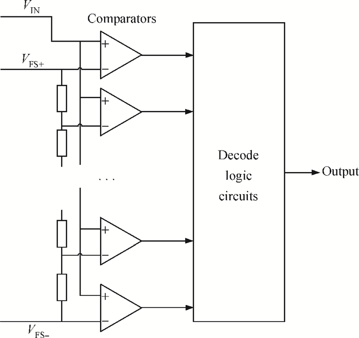
Fig. 1.
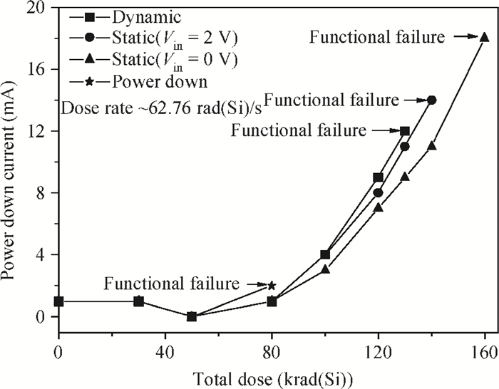
The relationship between the power-down current and the total dose under four conditions.
SEMICONDUCTOR DEVICES
Xue Wu1, 2, 3, , Wu Lu1, 2, Yudong Li1, 2, 3, Qi Guo1, 2, Xin Wang1, 2, 3, Xingyao Zhang1, 2, 3, Xin Yu1, 2 and Wuying Ma1, 2, 3
Corresponding author: Wu Xue, Email:xuew86@gmail.com
Abstract: This paper presents the total ionizing dose test results at different biases and dose rates for AD9233, which is fabricated using a modern CMOS process. The experimental results show that the digital parts are more sensitive than the other parts. Power down is the worst-case bias, and this phenomenon is first found in the total ionizing dose effect of analog-to-digital converters. We also find that the AC as well as DC parameters are sensitive to the total ionizing dose at a high dose rate, whereas none of the parameters are sensitive at a low dose rate. The test facilities, results and analysis are presented in detail.
Keywords: ionizing radiation, analog-to-digital converter, different biases, dose-rate effects
| [1] |
Lee C I, Rax B G, Johnston A H. Total ionizing dose effects in 12-bit successive-approximation analog-to-digital converters. IEEE Workshop Record, Radiation Effects Data Workshop, 1993:112 http://ieeexplore.ieee.org/xpls/abs_all.jsp?arnumber=700576
|
| [2] |
Turflinger T L, Davey M V, Bings J P. Radiation effects in analog CMOS analog-to-digital converters. IEEE Workshop Record, Radiation Effects Data Workshop, 1996:6 http://ieeexplore.ieee.org/xpls/abs_all.jsp?arnumber=574182
|
| [3] |
Lee C I, Rax B G, Johnston A H. Total ionizing dose effects in high resolution (12-/14-bit) analog-to-digital converters. IEEE Trans Nucl Sci, 1994, 41(6):2459 doi: 10.1109/23.340602
|
| [4] |
Lee C I, Rax B G, Johnston A H. Hardness assurance and testing techniques for high resolution (12 to 16-bit) analog-to-digital converters. IEEE Trans Nucl Sci, 1995, 42(6):1681 doi: 10.1109/23.488766
|
| [5] |
Black J D, Eaton P H, Chavez J R, et al. Total dose evaluation of state-of-the-art commercial analog to digital converters for space-based imaging applications. IEEE Work shop Record, Radiation Effects Data Workshop, 1998:121 http://ieeexplore.ieee.org/xpls/abs_all.jsp?arnumber=731490
|
| [6] |
Guo Qi, Ren Diyuan, Fan Long, et al. Ionizing radiation effect of analog to digital converters. Nucl Tech, 1997, 20(1):753 http://www.en.cnki.com.cn/Article_en/CJFDTOTAL-HJSU701.005.htm
|
| [7] |
Wu Xue, Lu Wu, Wang Yiyuan, et al. Total ionizing dose effects on a radiation-induced BiMOS analog-to-digital converter. Journal of Semiconductors, 2013, 34(1):015006 doi: 10.1088/1674-4926/34/1/015006
|
| [8] |
Witczak S C, Lacoe R C, Osborn J V, et al. Dose rate sensitivity of modern nMOSFETs. IEEE Trans Nucl Sci, 2005, 52(6):2602 doi: 10.1109/TNS.2005.860709
|
| [9] |
Zebrev G I, Gorbunov M S. Modeling of radiation-induced leakage and low dose-rate effects in thick edge isolation of modern MOSFETs. IEEE Trans Nucl Sci, 2009, 56(4):2230 doi: 10.1109/TNS.2009.2016096
|
| [10] |
Faccio F, Cervelli G. Radiation-induced edge effects in deep submicron CMOS transistors. IEEE Nucl Plasma Sciences Soc, 2005, 52(6):2413 http://ieeexplore.ieee.org/document/1589217/
|
| [11] |
Liu Zhangli, Hu Zhenyuan, Zhang Zhengxuan, et al. Gate length dependence of the shallow trench isolation leakage current in an irradiated deep submicron NMOSFET. Journal of Semiconductors, 2011, 32(6):064004 doi: 10.1088/1674-4926/32/6/064004
|
| [12] |
Faccio F, Barnaby H J, Chen X J, et al. Total ionizing dose effects in shallow trench isolation oxides. Microelectron Reliab, 2008, 48(7):1000 doi: 10.1016/j.microrel.2008.04.004
|
| [13] |
Barnaby H J. Total-ionizing-dose effects in modern CMOS technologies. IEEE Nucl Plasma Sci Soc, 2006, 53(6):3103 doi: 10.1109/TNS.2006.885952
|
| [14] |
Razavi B. Design of analog CMOS integrated circuits. New York:The McGraw-Hill Press, 2001
|
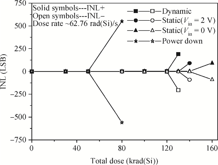
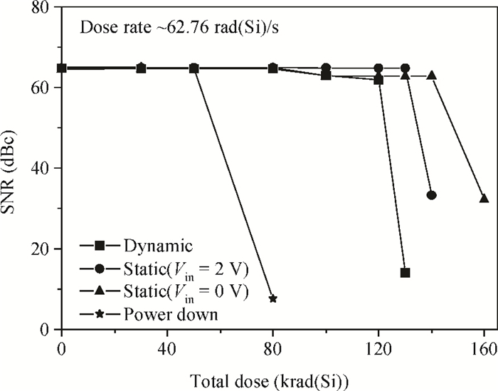
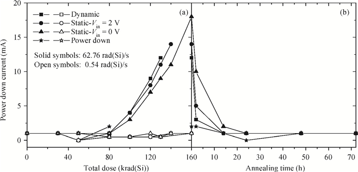
Table 1. Electrical test conditions.

|
Table 2. Irradiation biases.

|
Table 3. Other parameter results at pre-and post-irradiation, and room-temperature annealing.

|
| [1] |
Lee C I, Rax B G, Johnston A H. Total ionizing dose effects in 12-bit successive-approximation analog-to-digital converters. IEEE Workshop Record, Radiation Effects Data Workshop, 1993:112 http://ieeexplore.ieee.org/xpls/abs_all.jsp?arnumber=700576
|
| [2] |
Turflinger T L, Davey M V, Bings J P. Radiation effects in analog CMOS analog-to-digital converters. IEEE Workshop Record, Radiation Effects Data Workshop, 1996:6 http://ieeexplore.ieee.org/xpls/abs_all.jsp?arnumber=574182
|
| [3] |
Lee C I, Rax B G, Johnston A H. Total ionizing dose effects in high resolution (12-/14-bit) analog-to-digital converters. IEEE Trans Nucl Sci, 1994, 41(6):2459 doi: 10.1109/23.340602
|
| [4] |
Lee C I, Rax B G, Johnston A H. Hardness assurance and testing techniques for high resolution (12 to 16-bit) analog-to-digital converters. IEEE Trans Nucl Sci, 1995, 42(6):1681 doi: 10.1109/23.488766
|
| [5] |
Black J D, Eaton P H, Chavez J R, et al. Total dose evaluation of state-of-the-art commercial analog to digital converters for space-based imaging applications. IEEE Work shop Record, Radiation Effects Data Workshop, 1998:121 http://ieeexplore.ieee.org/xpls/abs_all.jsp?arnumber=731490
|
| [6] |
Guo Qi, Ren Diyuan, Fan Long, et al. Ionizing radiation effect of analog to digital converters. Nucl Tech, 1997, 20(1):753 http://www.en.cnki.com.cn/Article_en/CJFDTOTAL-HJSU701.005.htm
|
| [7] |
Wu Xue, Lu Wu, Wang Yiyuan, et al. Total ionizing dose effects on a radiation-induced BiMOS analog-to-digital converter. Journal of Semiconductors, 2013, 34(1):015006 doi: 10.1088/1674-4926/34/1/015006
|
| [8] |
Witczak S C, Lacoe R C, Osborn J V, et al. Dose rate sensitivity of modern nMOSFETs. IEEE Trans Nucl Sci, 2005, 52(6):2602 doi: 10.1109/TNS.2005.860709
|
| [9] |
Zebrev G I, Gorbunov M S. Modeling of radiation-induced leakage and low dose-rate effects in thick edge isolation of modern MOSFETs. IEEE Trans Nucl Sci, 2009, 56(4):2230 doi: 10.1109/TNS.2009.2016096
|
| [10] |
Faccio F, Cervelli G. Radiation-induced edge effects in deep submicron CMOS transistors. IEEE Nucl Plasma Sciences Soc, 2005, 52(6):2413 http://ieeexplore.ieee.org/document/1589217/
|
| [11] |
Liu Zhangli, Hu Zhenyuan, Zhang Zhengxuan, et al. Gate length dependence of the shallow trench isolation leakage current in an irradiated deep submicron NMOSFET. Journal of Semiconductors, 2011, 32(6):064004 doi: 10.1088/1674-4926/32/6/064004
|
| [12] |
Faccio F, Barnaby H J, Chen X J, et al. Total ionizing dose effects in shallow trench isolation oxides. Microelectron Reliab, 2008, 48(7):1000 doi: 10.1016/j.microrel.2008.04.004
|
| [13] |
Barnaby H J. Total-ionizing-dose effects in modern CMOS technologies. IEEE Nucl Plasma Sci Soc, 2006, 53(6):3103 doi: 10.1109/TNS.2006.885952
|
| [14] |
Razavi B. Design of analog CMOS integrated circuits. New York:The McGraw-Hill Press, 2001
|


Article views: 3884 Times PDF downloads: 21 Times Cited by: 0 Times
Received: 25 September 2013 Revised: 01 November 2013 Online: Published: 01 April 2014
| Citation: |
Xue Wu, Wu Lu, Yudong Li, Qi Guo, Xin Wang, Xingyao Zhang, Xin Yu, Wuying Ma. The total ionizing dose effect in 12-bit, 125 MSPS analog-to-digital converters[J]. Journal of Semiconductors, 2014, 35(4): 044008. doi: 10.1088/1674-4926/35/4/044008
****
X Wu, W Lu, Y D Li, Q Guo, X Wang, X Y Zhang, X Yu, W Y Ma. The total ionizing dose effect in 12-bit, 125 MSPS analog-to-digital converters[J]. J. Semicond., 2014, 35(4): 044008. doi: 10.1088/1674-4926/35/4/044008.

|
| [1] |
Lee C I, Rax B G, Johnston A H. Total ionizing dose effects in 12-bit successive-approximation analog-to-digital converters. IEEE Workshop Record, Radiation Effects Data Workshop, 1993:112 http://ieeexplore.ieee.org/xpls/abs_all.jsp?arnumber=700576
|
| [2] |
Turflinger T L, Davey M V, Bings J P. Radiation effects in analog CMOS analog-to-digital converters. IEEE Workshop Record, Radiation Effects Data Workshop, 1996:6 http://ieeexplore.ieee.org/xpls/abs_all.jsp?arnumber=574182
|
| [3] |
Lee C I, Rax B G, Johnston A H. Total ionizing dose effects in high resolution (12-/14-bit) analog-to-digital converters. IEEE Trans Nucl Sci, 1994, 41(6):2459 doi: 10.1109/23.340602
|
| [4] |
Lee C I, Rax B G, Johnston A H. Hardness assurance and testing techniques for high resolution (12 to 16-bit) analog-to-digital converters. IEEE Trans Nucl Sci, 1995, 42(6):1681 doi: 10.1109/23.488766
|
| [5] |
Black J D, Eaton P H, Chavez J R, et al. Total dose evaluation of state-of-the-art commercial analog to digital converters for space-based imaging applications. IEEE Work shop Record, Radiation Effects Data Workshop, 1998:121 http://ieeexplore.ieee.org/xpls/abs_all.jsp?arnumber=731490
|
| [6] |
Guo Qi, Ren Diyuan, Fan Long, et al. Ionizing radiation effect of analog to digital converters. Nucl Tech, 1997, 20(1):753 http://www.en.cnki.com.cn/Article_en/CJFDTOTAL-HJSU701.005.htm
|
| [7] |
Wu Xue, Lu Wu, Wang Yiyuan, et al. Total ionizing dose effects on a radiation-induced BiMOS analog-to-digital converter. Journal of Semiconductors, 2013, 34(1):015006 doi: 10.1088/1674-4926/34/1/015006
|
| [8] |
Witczak S C, Lacoe R C, Osborn J V, et al. Dose rate sensitivity of modern nMOSFETs. IEEE Trans Nucl Sci, 2005, 52(6):2602 doi: 10.1109/TNS.2005.860709
|
| [9] |
Zebrev G I, Gorbunov M S. Modeling of radiation-induced leakage and low dose-rate effects in thick edge isolation of modern MOSFETs. IEEE Trans Nucl Sci, 2009, 56(4):2230 doi: 10.1109/TNS.2009.2016096
|
| [10] |
Faccio F, Cervelli G. Radiation-induced edge effects in deep submicron CMOS transistors. IEEE Nucl Plasma Sciences Soc, 2005, 52(6):2413 http://ieeexplore.ieee.org/document/1589217/
|
| [11] |
Liu Zhangli, Hu Zhenyuan, Zhang Zhengxuan, et al. Gate length dependence of the shallow trench isolation leakage current in an irradiated deep submicron NMOSFET. Journal of Semiconductors, 2011, 32(6):064004 doi: 10.1088/1674-4926/32/6/064004
|
| [12] |
Faccio F, Barnaby H J, Chen X J, et al. Total ionizing dose effects in shallow trench isolation oxides. Microelectron Reliab, 2008, 48(7):1000 doi: 10.1016/j.microrel.2008.04.004
|
| [13] |
Barnaby H J. Total-ionizing-dose effects in modern CMOS technologies. IEEE Nucl Plasma Sci Soc, 2006, 53(6):3103 doi: 10.1109/TNS.2006.885952
|
| [14] |
Razavi B. Design of analog CMOS integrated circuits. New York:The McGraw-Hill Press, 2001
|

 WeChat ID
Journal of Semiconductors © 2017 All Rights Reserved 京ICP备05085259号-2

 DownLoad: